

Page 1

SPECIFICATION FOR APPROVAL
Customer : MSI
Part No : S93-0408230-D04 Rev :
Description : ADAPTER
Delta Model No : ADP-36CH AH Rev : 00
Sample Issue Date : Feb. 12 , 2009
DELTA ELECTRONICS, INC.
3, Tung Yuan Road
Chungli Industrial Zone.
Taoyuan Hsien 320, Taiwan, R.O.C
Internet : http:/www.deltaww.com
TEL:886-3-4526107 FAX:886-3-4343617
Page 2
TABLE OF CONTENTS
1. Revision History
2. Electrical Specification
3. Schematic
4. PCB Artwork
5. Physical Dimension
6. Label Drawing
7. Packing
8. BOM (Part List)
9. Safety License
Please send one copy of this specification back after you signed
approval for production pre-arrangement.
Approved By :
Date :
Engineer By:Danny Chen M.Engineer By: Aaron Yang Approved By: Jimmy Chiang _
Page 3
1. Revision History
Page 4

DELTA P/N ADP-36CH AH SHEET 1 OF 1
CONTENT Revision History DATE Feb. 12 ,2009
1.Revision History
REV. DESCRIPTION ENGINEER DATE
--------------------------------------------------------------------------------------------------------------- 00 ISSUE Danny Chen 02/12/2009
Page 5
2. Electrical Specification
Page 6
1. Electrical
1.1 Input Characteristics Page
1.1.1 Nominal Voltage…………………………………….…………..…………….…………………… 4
1.1.2 Input Voltage Range………………………………….………………………….……………….. 4
1.1.3 Rated Frequency……………………………………………………………….………………….. 4
1.1.4 Frequency Range……………………………………………………………….…………………. 4
1.1.5 Input current …………………………………………………………………………………………4
1.1.6 Inrush Current Limit(cold start)…………………………………………………………………….4
1.1.7 Efficiency ………………………………………………………………………...………………….4
1.1.8 No Load Power Consumption………………………………………………..…………. .…….….5
1.1.9 Small Load Power Consumption……………………………………………………… …………..5
1.2 Output Characteristics
1.2.1 Rated Voltage……………………………………………………………………………..……….. 5
1.2.2 Voltage Range ……………………………………………………………………………………...5
Table Of Contents
1.2.3 Current………………………………………………………………….……………….…………...5
1.2.4 Output Ripple and Noise………………………………………………………………………….. 5
1.2.5 Turn On delay time………………………………………………………………………………… 5
1.2.6 Hold – up Time…………………………………………………………………………………….. 5
1.2.7 Rise time…………..………………………………………………………………………………. 6
1.2.8 Surge load:………………………………………………………………………………………… 6
1.2.9 Load transient response…………………………………………………………………………. 6
1.2.10 Protection………………………………………………………………………………………….. .6
1.2.10.1 Over Voltage Protection…………………………………………………………………..6
1.2.10.2 Over Current Protection…………………………………………………………………..6
1.2.10.3 Short Circuit Protection……………………………………………………………….…..6
1.2.10.4 Over Temperature Protection…………………………………………………………….7
台達電子工業股份有限公司
DELTA ELECTRONICS, INC.
THESE DRAWINGS AND SPECIFICATIONS ARE THE PROPERTY OF DELTA
ELECTRONICS, INC. AND SHALL NOT BE REPRODUCED OR USED AS THE
BASIS FOR THE MANUFACTURE OR SELL OF APPARATUSES OR DEVICES
WITHOUT PERMISSION.
Date Drawn Design (EE) Design (ME)
12/18/2008
洪若蘭 陳俊志 楊基祥
DESCRIPTION :
電氣規格 (Electrical Specification)
MODEL NO. :
ADP-36CH AH
DOCUMENT NAME. :
ES-36CH AH
REV.
S00
File Name:DF-PSLA4V-2R00.DOC SHEET 2 OF 10
Page 7

2. Environmental
2.1 Temperature………………………………………………………………………………….…………….. 7
2.2 Humidity …………………………………………………………………………………………………….. 7
2.3 Immunity………………………………..…………………………………………………………………… 8
2.3.1 Lightning Surge Immunity………………………………………………………………………… 8
2.3.2 Electric Fast Transients (EFT)…………………………………………………… ……………… 8
2.4 Electrostatic Discharge (ESD)………..………………………..…………………………………… …….. 8
2.5 Surface Temperature rise……..…………………………………………………………………………….8
2.6 Dielectric Withstand Voltage (HI-POT)……..……………………………………………………………. 8
2.7 Leakage Current.…………………………….…………………………………………………………….. 8
2.8 Insulation Resistance……………………………….……………………………………………………… 8
2.9 Electromagnetic Interference (EMI).…..…………………………………………………………………. 9
2.10 MTBF………………………………………………………………………………………………………… 9
3.
Mechanical
3.1 Outline Dimension……………………………………………………………………………….…………. 10
3.2 AC Inlet type………………………………………………………………………………………………… 10
3.3 DC Cable Length……………………………………………………………………………….……………10
3.4 DC Cable Type …………………………………………………………………… ……………………..….10
3.5 DC Connector Dimension..…………………………………………………………………………………10
台達電子工業股份有限公司
DELTA ELECTRONICS, INC.
THESE DRAWINGS AND SPECIFICATIONS ARE THE PROPERTY OF DELTA
ELECTRONICS, INC. AND SHALL NOT BE REPRODUCED OR USED AS THE
BASIS FOR THE MANUFACTURE OR SELL OF APPARATUSES OR DEVICES
WITHOUT PERMISSION.
Date Drawn Design (EE) Design (ME)
12/18/2008
洪若蘭 陳俊志 楊基祥
DESCRIPTION :
電氣規格 (Electrical Specification)
MODEL NO. :
ADP-36CH AH
DOCUMENT NAME. :
ES-36CH AH
REV.
S00
File Name:DF-PSLA4V-2R00.DOC SHEET 3 OF 10
Page 8

1. ELECTRICAL
1.1 Input Characteristics:
1.1.1
1.1.2 Input Voltage Range
1.1.3 Rated Frequency
1.1.4 Frequency Range
1.1.5 Input Current
1.1.6 Inrush Current Limit (cold start)
1.1.7
Nominal Voltage
It is normal for 100 ~ 240Vac input AC voltage.
The Adapter shall operate from 90 ~ 264Vac.
It is normal for 50Hz or 60Hz and single phase.
The Adapter shall operate with an input frequency from 47 Hz to 63 Hz.
1.2A Max at 100Vac input voltage.
No damage at 240Vac.
Efficiency (Warm Up)
1.1.7.1 83 % min. at nominal input voltage, maximum load and measured a t the end of DC cable.
1.1.7.2 Active mode efficiency:
More than 82.25% of average efficiency of 25%,50%,75% and 100% load tested at 115Vac and
230Vac. (Warm up after 30 minutes)
台達電子工業股份有限公司
DELTA ELECTRONICS, INC.
THESE DRAWINGS AND SPECIFICATIONS ARE THE PROPERTY OF DELTA
ELECTRONICS, INC. AND SHALL NOT BE REPRODUCED OR USED AS THE
BASIS FOR THE MANUFACTURE OR SELL OF APPARATUSES OR DEVICES
WITHOUT PERMISSION.
Date Drawn Design (EE) Design (ME)
12/18/2008
洪若蘭 陳俊志 楊基祥
DESCRIPTION :
電氣規格 (Electrical Specification)
MODEL NO. :
ADP-36CH AH
DOCUMENT NAME. :
ES-36CH AH
File Name:DF-PSLA4V-2R00.DOC SHEET 4 OF 10
REV.
S00
Page 9
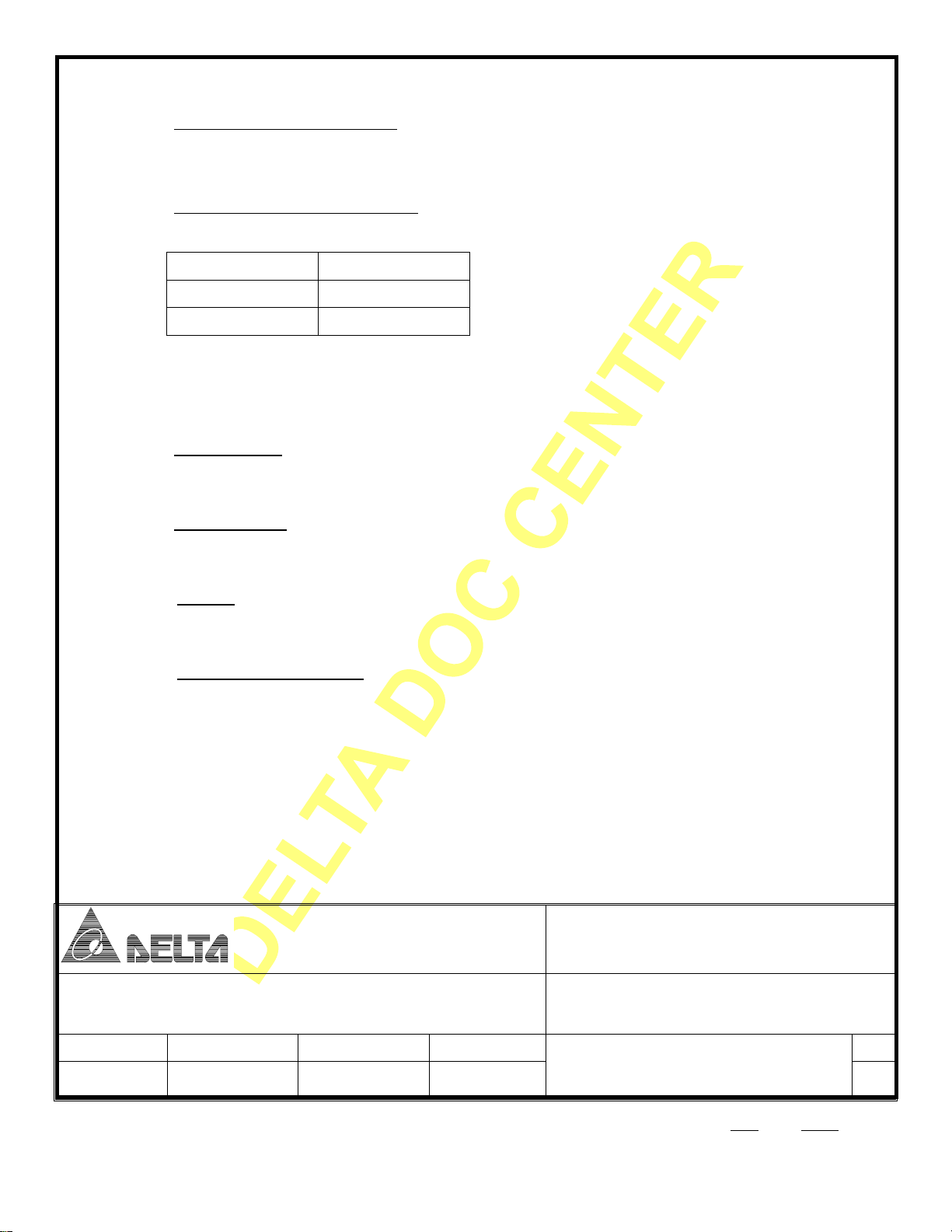
1.1.8 No Load Power Consumption
Maximum non-load power consumption is less than 0.5W at 115Vac/60Hz and 230Vac/50HZ
1.1.9 Small Load Power Consumption
Vin=115Vac/60Hz and 230Vac/50Hz
Output load(W) Input power (max)
1W 1.7W
1.5W 2.4W
1.2 Output Characteristics:
1.2.1 Rated Voltage
The rated output voltage is specified at 12V.
1.2.2 Voltage Range
The output voltage will be performed 11.4~ 12.6V when the load is 0A ~ 3A steadily.
1.2.3
1.2.4
Current
This Adapter can work from 0A to 3A and output voltage is in section 1.2.2 specified range.
Output Ripple and Noise
Output ripple voltage is 350 mV peak to peak or less.
Measured methods:
T1. Performed by 20M Hz bandwidth in oscilloscope.
T2. Applied 0.1uF high frequency capacitor and 10uF electrolytic capacitor across output connector terminals.
T3. Measured at the end of DC cable.
T4. 47Hz and 63Hz tested at 90Vac and 264Vac.
台達電子工業股份有限公司
DELTA ELECTRONICS, INC.
THESE DRAWINGS AND SPECIFICATIONS ARE THE PROPERTY OF DELTA
ELECTRONICS, INC. AND SHALL NOT BE REPRODUCED OR USED AS THE
BASIS FOR THE MANUFACTURE OR SELL OF APPARATUSES OR DEVICES
WITHOUT PERMISSION.
Date Drawn Design (EE) Design (ME)
12/18/2008
洪若蘭 陳俊志 楊基祥
DESCRIPTION :
電氣規格 (Electrical Specification)
MODEL NO. :
ADP-36CH AH
DOCUMENT NAME. :
ES-36CH AH
File Name:DF-PSLA4V-2R00.DOC SHEET 5 OF 10
REV.
S00
Page 10
1.2.5 Turn On delay time
The Adapter shall switch on in less than 2 seconds at input voltage is 100Vac.
1.2.6 Hold –up time
The output voltage shall be sustained 6mS within regulation requirement after loss 100Vac and maximum load.
1.2.7 Rise time
DC output rise time from 10% to 90% of output voltage shall be less than 40ms at nominal line
and maximum load
1.2.8 Surge load:
The adapter shall support a surge load with 110% of maximum load for 1mS.
1.2.9 Load transient response
The adapter must within regulation when applied a step load from 0% to 50% and 50% to 100%
load at 0.5A/us slew rate and 10mS time period.
The output voltage
1.2.10 Protection
1.2.10.1 Over Voltage Protection
will be performed 11.4~ 12.6V.
The output shall be protected to latch off at over-voltage condition, maximum value can’t be over 20V.
That might be return to normal state by AC reset, reset ≤ 2 Minutes.
1.2.10.2 Over Current Protection
The maximum constant current shall be less than 5A.
The ADAPTOR SHALL BE AUTO-RECOVERY.
台達電子工業股份有限公司
DELTA ELECTRONICS, INC.
THESE DRAWINGS AND SPECIFICATIONS ARE THE PROPERTY OF DELTA
ELECTRONICS, INC. AND SHALL NOT BE REPRODUCED OR USED AS THE
BASIS FOR THE MANUFACTURE OR SELL OF APPARATUSES OR DEVICES
WITHOUT PERMISSION.
Date Drawn Design (EE) Design (ME)
12/18/2008
洪若蘭 陳俊志 楊基祥
DESCRIPTION :
電氣規格 (Electrical Specification)
MODEL NO. :
ADP-36CH AH
DOCUMENT NAME. :
ES-36CH AH
File Name:DF-PSLA4V-2R00.DOC SHEET 6 OF 10
REV.
S00
Page 11

1.2.10.3 Short Circuit protection
Output can be shorted without damage. The adaptor shall be auto-recovery. (It will enter into norm al
condition when the fault condition is removed.)
1.2.10.4 Over Temperature Protection
No deformation and no discoloration on case and will be shut down. That will be return to normal state
by ac reset, reset≦2 minutes.
2. Environmental
2.1 Temperature
2.1.1 Operating
The AC Adapter shall be capable of operating at full load with an ambient temperature range of 0 ℃
to +40℃.
2.1.2 Shipping/Storage
The AC Adapter shall be capable of withstanding ambient temperature from -20℃ to +70℃.
2.2 Humidity
2.2.1 Operating
The AC Adapter shall be capable of operation in relative humidity of 10% to 90% relative humidity,
non-condensing.
2.2.2 Shipping/storage
The AC Adapter shall be capable of withstanding ambient relative humidity of 5% to 95% relative
humidity, non-condensing.
台達電子工業股份有限公司
DELTA ELECTRONICS, INC.
THESE DRAWINGS AND SPECIFICATIONS ARE THE PROPERTY OF DELTA
ELECTRONICS, INC. AND SHALL NOT BE REPRODUCED OR USED AS THE
BASIS FOR THE MANUFACTURE OR SELL OF APPARATUSES OR DEVICES
WITHOUT PERMISSION.
Date Drawn Design (EE) Design (ME)
12/18/2008
洪若蘭 陳俊志 楊基祥
DESCRIPTION :
電氣規格 (Electrical Specification)
MODEL NO. :
ADP-36CH AH
DOCUMENT NAME. :
ES-36CH AH
REV.
S00
File Name:DF-PSLA4V-2R00.DOC SHEET 7 OF 10
Page 12
2.3 Immunity
2.3.1 Lightning Surge Immunity
This is to follow the norm of IEC-1000-4-5 Level 3 requirements
L-N 1KV/1.2
2.3.2 Electric Fast Transients (EFT)
This is to follow the norm of IEC-61000-4-4/1995
(EN 61000-4-4) Level 3 requirements
* 50uS 5 times No function error.
2.4 Electrostatic Discharge ( ESD )
This Adapter is capable to withstand ESD test voltage at any point around the enclosure as below.
(Refer to IEC61000-4-2)
±12KV air discharge No damage.
±6KV contact discharge No damage.
2.5 Surface Temperature rise
Output 36W and ambient
35℃±3℃;input voltage 100Vac/240Vac case temperature rise≦45℃.
2.6 Dielectric Withstand Voltage ( HI – POT )
100% of line products of this Adapter shall be applied 3000Vac for 2 seconds between AC
input terminals and output terminals. Cut off current is 3mA.
2.7 Leakage Current :
The AC leakage current is less than 100μA when adapter is connected to 240Vac/60Hz at normal condition.
台達電子工業股份有限公司
DELTA ELECTRONICS, INC.
THESE DRAWINGS AND SPECIFICATIONS ARE THE PROPERTY OF DELTA
ELECTRONICS, INC. AND SHALL NOT BE REPRODUCED OR USED AS THE
BASIS FOR THE MANUFACTURE OR SELL OF APPARATUSES OR DEVICES
WITHOUT PERMISSION.
Date Drawn Design (EE) Design (ME)
12/18/2008
洪若蘭 陳俊志 楊基祥
DESCRIPTION :
電氣規格 (Electrical Specification)
MODEL NO. :
ADP-36CH AH
DOCUMENT NAME. :
ES-36CH AH
File Name:DF-PSLA4V-2R00.DOC SHEET 8 OF 10
REV.
S00
Page 13
2.8 Insulation Resistance
The insulation resistance shall be not less than 30M ohms after application of 500Vdc/10mA for 1 minute.
2.9 Electromagnetic Interference (EMI)
2.9.1 The adapter shall comply with the following national standards.
(a) CISPR 22 Class B
VCCI Class B
(b)
2.10 MTBF
2.10.1 MTBF(Mean-Time-Between-Failures)Calculation
2.10.2 MTBF Verification
The calculated MTBF shall be 150,000 hours of continuous operation at 25℃,
maximum load and normal voltage.
The MTBF shall be verified from life testing performed by factory Quality department.
The operating conditions are:40℃ambient temperature, sea level ,both nominal line voltage
ranges(110VAC or 220VAC) and a minimum load of 75% of the maximum load.
台達電子工業股份有限公司
DELTA ELECTRONICS, INC.
THESE DRAWINGS AND SPECIFICATIONS ARE THE PROPERTY OF DELTA
ELECTRONICS, INC. AND SHALL NOT BE REPRODUCED OR USED AS THE
BASIS FOR THE MANUFACTURE OR SELL OF APPARATUSES OR DEVICES
WITHOUT PERMISSION.
Date Drawn Design (EE) Design (ME)
12/18/2008
洪若蘭 陳俊志 楊基祥
DESCRIPTION :
電氣規格 (Electrical Specification)
MODEL NO. :
ADP-36CH AH
DOCUMENT NAME. :
ES-36CH AH
File Name:DF-PSLA4V-2R00.DOC SHEET 9 OF 10
REV.
S00
Page 14

3. Mechanical
3.1 Outline Dimension: 96.0*42.0*28.7 mm , Color : Black
3.2 AC Inlet type:
3.3 DC Cable Length:
3.4 DC Cable Type
3.5 DC Connector Dimension:
OD= 5.5 mm
ID= 1.7 mm
Length= 12.5 mm
Socket C8 type
1800 mm
: UL1571, AWG #18
台達電子工業股份有限公司
DELTA ELECTRONICS, INC.
THESE DRAWINGS AND SPECIFICATIONS ARE THE PROPERTY OF DELTA
ELECTRONICS, INC. AND SHALL NOT BE REPRODUCED OR USED AS THE
BASIS FOR THE MANUFACTURE OR SELL OF APPARATUSES OR DEVICES
WITHOUT PERMISSION.
Date Drawn Design (EE) Design (ME)
12/18/2008
洪若蘭 陳俊志 楊基祥
DESCRIPTION :
電氣規格 (Electrical Specification)
MODEL NO. :
ADP-36CH AH
DOCUMENT NAME. :
ES-36CH AH
File Name:DF-PSLA4V-2R00.DOC SHEET 10 OF 10
REV.
S00
Page 15
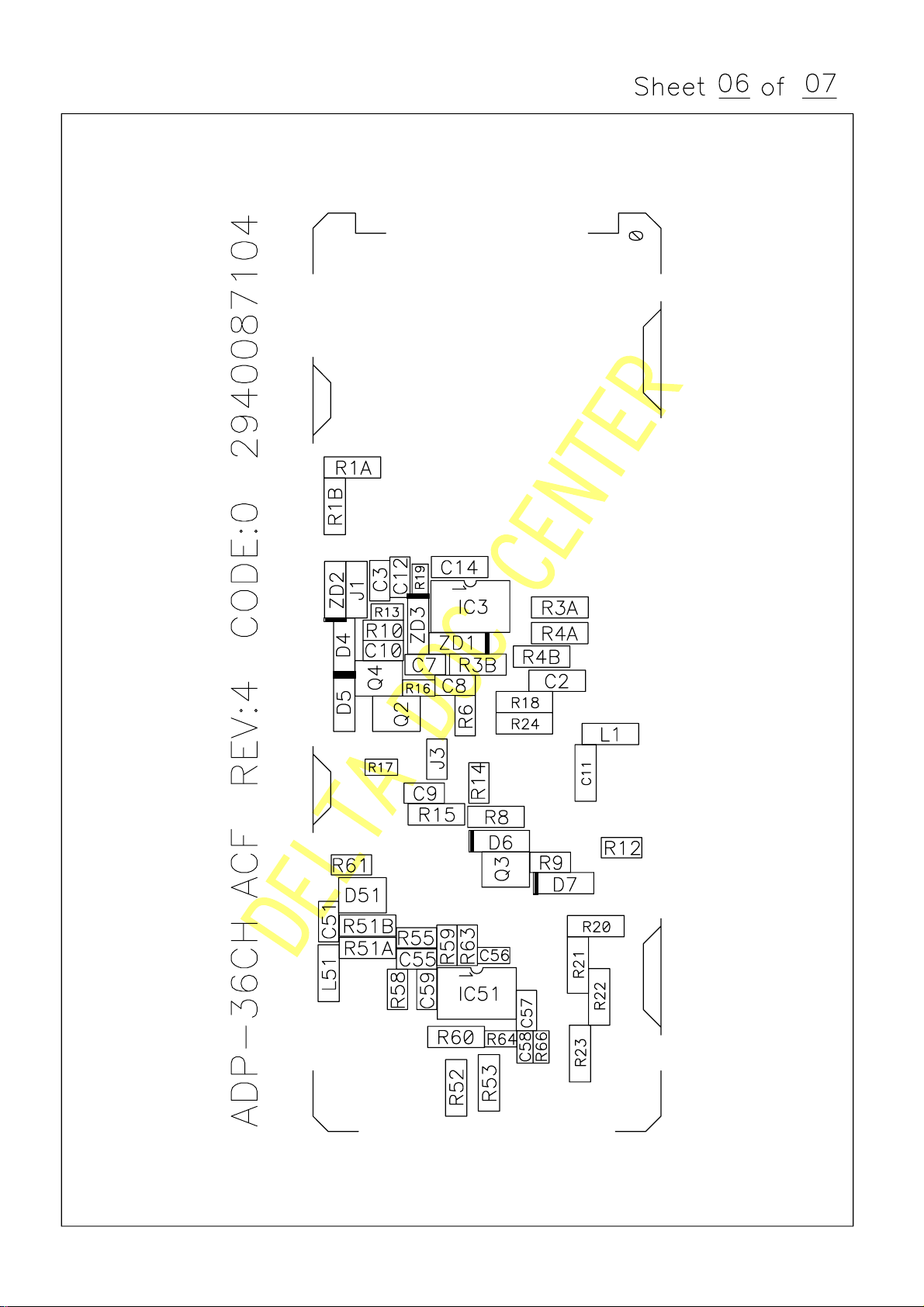
3.Schematic
Page 16
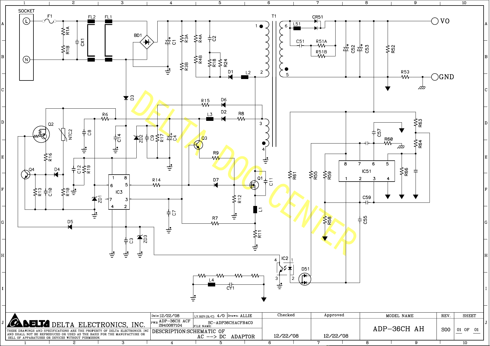
C56
C58
R20 R22 R2 3
R21
陳俊志 蔣進財
Page 17

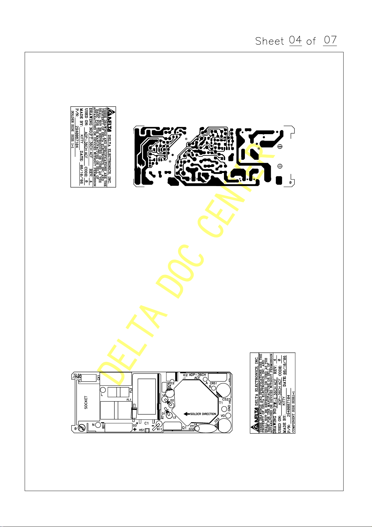
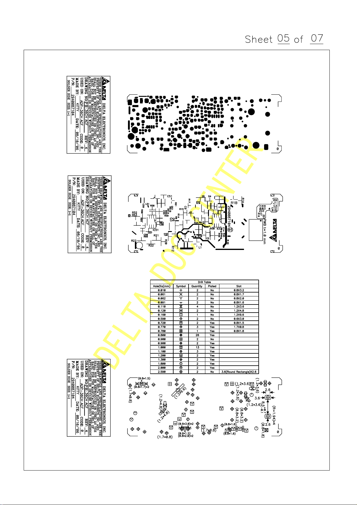
4. PCB Artwork
Page 18
Page 19
Page 20
Page 21

5.Physical Dimension
Page 22

Page 23
6.Label Drawing
Page 24
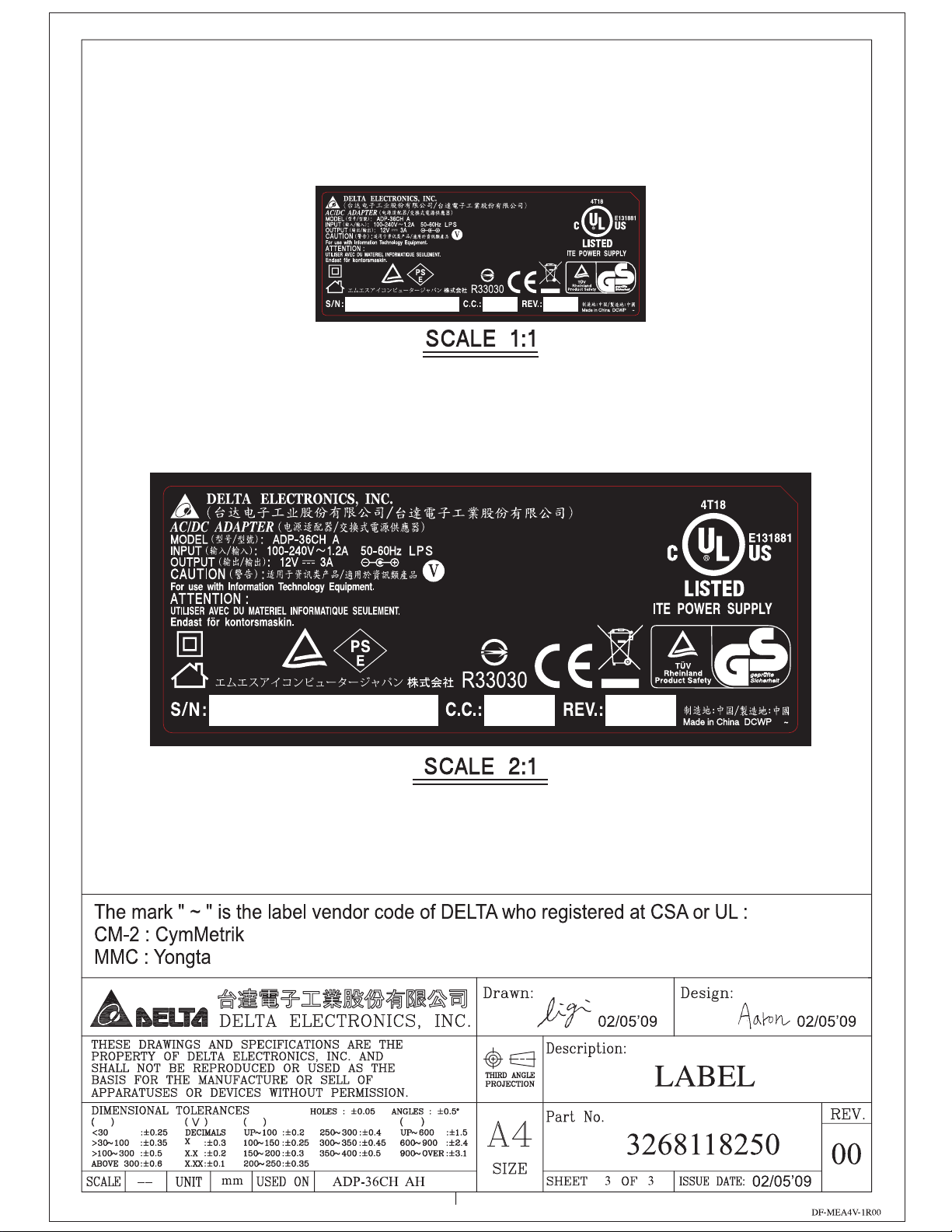
Page 25
7.Packing
Page 26
Page 27

8. BOM (Part list)
Page 28

R
L
R
L
O
O
T
S
S
O
< ADP-36CH AH CUSTOMER BOM LIST >
DATE: 01/21/2009
DESCRIPTION MFG NAME MFG PART % QPA UNIT DESIGN NO Item text 1
RES CF 1/4W 2.7Kohm J SMALL KAMAYA 1.000 PCE R7
RES MOF 1W 560mohm J SMALL FR FUTABA 1.000 PCE R11
FUSE T S 2.5A 250V L BEL FUSE LIMITED RST 2.5 0 1.000 PCE F1
FUSE T S 2.5A 250VAC L LITTELFUSE FAR EAST PTE LTD. 392-2.5A 0 1.000 PCE F1
FUSE T S 2.5A 250V L CONQUER ELEC.CO.,LTD MST2.5 0 1.000 PCE F1
FUSE T S 2.5A 250VAC L Walter Electronic Co Ltd 2010T2.5A 100 1.000 PCE F1
RES NTC 470Kohm J 5200K +/-7% UPPERMOST ELECTRONIC INDUST
RES NTC 470Kohm J 5200K +/-7% THINKING ELECTRONIC INDUSTRIA
RES NTC 470Kohm J 5200K +/-5% TRA UPPERMOST ELECTRONIC INDUST
RES NTC 470Kohm J 5200K TRA THINKING ELECTRONIC INDUSTRIA
CAP Y1/X1 CD 250VAC 680pF K B VI10 MURATA MANUFACTURING CO.LTD DE1B3KX681KA4BL01 0 1.000 PCE CY1
CAP Y1/X1 CD 250VAC 680pF K B VI10 WALSIN TECHNOLOGY CORPORATI
CAP Y1/X1 CD 250VAC 680pF M E VI10 TDK Corporation CD75-E2GA681MYGS 0 1.000 PCE CY1
CAP Y1/X1 CD 250VAC 680pF K B TP VI10 MURATA MANUFACTURING CO.LTD DE1B3KX681KN4AL01 0 1.000 PCE CY1
CAP Y1/X1 CD 250VAC 680pF K B TP VI10 WALSIN TECHNOLOGY CORPORATI
CAP Y1/X1 CD 250VAC 680pF M E TP VI10 TDK Corporation CD75-E2GA681MYVS 100 1.000 PCE CY1
CAP AL LD 25V 330uF M 8*15 P3.5 NICHICON CORPORATION UHD1E331MPD1CV 100 1.000 PCE C52
CAP AL LD 25V 330uF M 8*15 P3.5 NICHICON CORPORATION UHD1E331MPD1CV 100 1.000 PCE C53
CAP AL LD 25V 330uF M 8*15 P3.5 TAICON CORPORATION THD1E331MK08150CK3 0 1.000 PCE C52
CAP AL LD 25V 330uF M 8*15 P3.5 TAICON CORPORATION THD1E331MK08150CK3 0 1.000 PCE C53
CAP AL LD 25V 330uF M 8*15 P3.5 NIPPON CHEMI-CON CORPORATION EKZE250EC3331MH15D 0 1.000 PCE C52
CAP AL LD 25V 330uF M 8*15 P3.5 NIPPON CHEMI-CON CORPORATION EKZE250EC3331MH15D 0 1.000 PCE C53
CAP AL LD 25V 330uF M 8*16 P3.5 RUBYCON CORPORATION 25ZL330MEFCCE8*16 0 1.000 PCE C52
CAP AL LD 25V 330uF M 8*16 P3.5 RUBYCON CORPORATION 25ZL330MEFCCE8*16 0 1.000 PCE C53
CAP AL LD 35V 33uF M 5*11 TP P5 NICHICON CORPORATION UPW1V330MDD1TA 0 1.000 PCE C4
CAP AL LD 35V 33uF M 5*11 TP P5 TAICON CORPORATION TPW1V330MK05110TC1 100 1.000 PCE C4
CAP AL LD 35V 33uF M 5*11 TP P5 LUMINOUS TOWN ELECTRIC CO., LT ZGD1VM330D11A 0 1.000 PCE C4
CAP AL LD 35V 33uF M 5*11 TP P5 RUBYCON CORPORATION 35YXG33MEFCTA5*11 0 1.000 PCE C4
CAP AL LD 35V 33uF M 5*11 TP P5 NIPPON CHEMI-CON CORPORATION EKY-350ETC330ME11D 0 1.000 PCE C4
CAP AL 400V 68uF M 16*25 P7.5 NIPPON CHEMI-CON CORPORATION EKMG401ELL680ML25S 0 1.000 PCE C1
CAP AL 400V 68uF M 16*25 P7.5 NICHICON CORPORATION UPT2G680MHD3 0 1.000 PCE C1
CAP AL 400V 68uF M 16*25 P7.5 LUMINOUS TOWN ELECTRIC CO., LT TYJ2GM680K25O 100 1.000 PCE C1
CAP X2 MP PC 275VAC 0.33uF K P15 HUA JUNG COMPONENTS CO., LTD. MKP-334K0275AB1151 0 1.000 PCE CX1
CAP X2 MP PC 275VAC 0.33uF M P15 ARCOTRONICS ITALIA SPA R46KI333045M 0 1.000 PCE CX1
CAP X2 MP PC 300VAC 0.33uF K S15 OKAYA HONG KONG TRADING LTD. LE334-MX-30-C3.2 100 1.000 PCE CX1
DIO BRD 2A 800V D3K-4P SHINDENGEN ELECTRIC MANUFAC
DIO FRD 1A 1000V DO-41-2P 500nS FAGOR ELECTRONICA, S. COOP RGP10MAMP 0 1.000 PCE D1
DIO FRD 1A 1000V DO-41-2P 500nS VISHAY SEMICONDUCTOR RGP10M-E3/73 0 1.000 PCE D1
DIO FRD 1A 1000V DO-41-2P 500nS PAN JIT INTERNATIONAL INC. PG1010R T/B 100 1.000 PCE D1
DIO SBD 10A 100V TO-220AB-3P C.C. STMicroelectronics Asia Pacific Pte STPS10H100CT 100 1.000 PCE CR51
DIO SBD 10A 100V TO-220AB-3P C.C. PAN JIT INTERNATIONAL INC. SB10100CT 0 1.000 PCE CR51
DIO SI 1A 1KV DO-41-2P FAIRCHILD SEMICONDUCTOR HK LT 1N4007 0 1.000 PCE D2
DIO SI 1A 1KV DO-204AL-2P VISHAY SEMICONDUCTOR 1N4007-E3/73 0 1.000 PCE D2
DIO SI 1A 1KV DO-41-2P PAN JIT INTERNATIONAL INC. 1N4007 T/B 100 1.000 PCE D2
DIO SI 1A 1KV DO-41-2P Tianjin Zhong-Huan Semiconductor T1N4007 0 1.000 PCE D2
DIO SI 1A 1KV DO-41-2P GULF SEMICONDUCTOR LIMITED 1N4007-47L 0 1.000 PCE D2
DIO SI 1A 1KV DO-204AL-2P VISHAY SEMICONDUCTOR 1N4007-E3/73 1.000 PCE D3
PHOTO TR 40mA 80V 4P 150-300% 10.16mm NEC CORPORATION PS2561BL1-1-V-A(G) 0 1.000 PCE IC2
PHOTO TR 50mA 70V DIP-4P 160-300% SHARP ELECTRONIC COMPONENTS PC123Y92FZ0F 100 1.000 PCE IC2
FET 600V 6A 1.2ohm TO-220FP-3P STMicroelectronics Asia Pacific Pte STP6NK60ZFP 0 1.000 PCE Q1
FET 600V 6A 1.25ohm TO-220F-3P TOSHIBA CORP. 2SK3562(Q) 0 1.000 PCE Q1
FET 600V 7.5A 1.2ohm TO-220F-3P FAIRCHILD SEMICONDUCTOR HK LT FQPF8N60C 0 1.000 PCE Q1
FET 600V 6A 1.1ohm TO-220FI(LS)-3P SANYO ELECTRONIC CO.,LTD. 2SK2628LS 0 1.000 PCE Q1
FET 600V 7A 1.2ohm TO-220F-3P AUK CORPORATION STK0760F 100 1.000 PCE Q1
INDUCTOR CR T10 251uH MIN DELTA ELECTRONICS,INC. CR-10-NB84A 1.000 PCE FL2
TRANSFORMER MAIN RM10/18.1 580uH +/-5% DELTA ELECTRONICS,INC. SMT-RM10-NB2075D 1.000 PCE T1
LINE FILTER T14 10.3mH MIN DELTA ELECTRONICS,INC. HFV-NB7103 1.000 PCE FL1
CORE BEAD 2.5*1*3 33ohm F4D FENGHERYIN CORPORATION F4D RH 2.5*1.0*3 0 1.000 PCE L4 FOR CY1
CORE BEAD 2.5*1*3*2.5*2.5 33ohm W4B TAI-TECH ADVANCED ELECTRONIC
CORE BEAD 3.5*1.2*6*3.5*3.5 40ohm W5 TAI-TECH ADVANCED ELECTRONIC
CORE BEAD 3.5*1.2*6 40ohm F7D FENGHERYIN CORPORATION F7D RH 3.5*1.2*6 0 1.000 PCE L2 FOR D1
RES SMD 1/4W 0ohm J 1206 KAMAYA 100 1.000 PCE J1
RES SMD 1/4W 0ohm J 1206 WALSIN TECHNOLOGY CORPORATI
ROYAL
TY-OHM
YAGEO
KOA
TDC05D447J(TDC05D447)-5m1 100 1.000 PCE NTC2
TTC05474JSY751(TTC474) 0 1.000 PCE NTC2
TDC05D447J-5X1TAmlhf 0 1.000 PCE NTC2
TTC05474JIYDA1 0 1.000 PCE NTC2
AH10B681KD0L-S 0 1.000 PCE CY1
AH10B681KD0LM-S 0 1.000 PCE CY1
UD2KB80-7000 1.000 PCE BD1
W4B RH2.5*3.0*1.0 100 1.000 PCE L4 FOR CY1
BRH3.5*6*1.2 100 1.000 PCE L2 FOR D1
ROYAL
TA-I
YAGEO
WR12X000 PTL 0 1.000 PCE J1
REV: 00
Page 29

< ADP-36CH AH CUSTOMER BOM LIST >
O
O
O
O
O
O
O
O
O
O
O
O
O
O
O
O
DATE: 01/21/2009
DESCRIPTION MFG NAME MFG PART % QPA UNIT DESIGN NO Item text 1
RES SMD 1/4W 100ohm J 1206 KAMAYA 100 1.000 PCE R18
RES SMD 1/4W 100ohm J 1206 KAMAYA 100 1.000 PCE R24
RES SMD 1/4W 100ohm J 1206 KAMAYA 100 1.000 PCE R51A
RES SMD 1/4W 100ohm J 1206 KAMAYA 100 1.000 PCE R51B
RES SMD 1/4W 100ohm J 1206 WALSIN TECHNOLOGY CORPORATI
RES SMD 1/4W 100ohm J 1206 WALSIN TECHNOLOGY CORPORATI
RES SMD 1/4W 100ohm J 1206 WALSIN TECHNOLOGY CORPORATI
RES SMD 1/4W 100ohm J 1206 WALSIN TECHNOLOGY CORPORATI
RES SMD 1/4W 100Kohm J 1206 KAMAYA 0 1.000 PCE R4A
RES SMD 1/4W 100Kohm J 1206 KAMAYA 0 1.000 PCE R4B
RES SMD 1/4W 100Kohm J 1206 WALSIN TECHNOLOGY CORPORATI
RES SMD 1/4W 100Kohm J 1206 WALSIN TECHNOLOGY CORPORATI
RES SMD 1/4W 1.5Kohm J 1206 KAMAYA 0 1.000 PCE R52
RES SMD 1/4W 1.5Kohm J 1206 WALSIN TECHNOLOGY CORPORATI
RES SMD 1/4W 1.5Mohm J 1206 KAMAYA 0 1.000 PCE R1A
RES SMD 1/4W 1.5Mohm J 1206 KAMAYA 0 1.000 PCE R1B
RES SMD 1/4W 1.5Mohm J 1206 KAMAYA 0 1.000 PCE R3B
RES SMD 1/4W 1.5Mohm J 1206 WALSIN TECHNOLOGY CORPORATI
RES SMD 1/4W 1.5Mohm J 1206 WALSIN TECHNOLOGY CORPORATI
RES SMD 1/4W 1.5Mohm J 1206 WALSIN TECHNOLOGY CORPORATI
RES SMD 1/4W 160ohm J 1206 KAMAYA 0 1.000 PCE R15
RES SMD 1/4W 160ohm J 1206 WALSIN TECHNOLOGY CORPORATI
RES SMD 1/4W 1.8Mohm J 1206 KAMAYA 100 1.000 PCE R3A
RES SMD 1/4W 1.8Mohm J 1206 WALSIN TECHNOLOGY CORPORATI
RES SMD 1/4W 5.1Kohm J 1206 KAMAYA 100 1.000 PCE R60
RES SMD 1/4W 5.1Kohm J 1206 WALSIN TECHNOLOGY CORPORATI
RES SMD 1/4W 8.2ohm J 1206 KAMAYA 0 1.000 PCE R8
RES SMD 1/4W 8.2ohm J 1206 WALSIN TECHNOLOGY CORPORATI
RES SMD 1/2W 10mohm F 1206 CYNTEC CO.,LTD. RL1632L R010 FN 1.000 PCE R53
RES SMD 1/10W 10Kohm F 0603 KAMAYA 0 1.000 PCE R16
RES SMD 1/10W 10Kohm F 0603 KAMAYA 0 1.000 PCE R17
RES SMD 1/10W 10Kohm F 0603 WALSIN TECHNOLOGY CORPORATI
RES SMD 1/10W 10Kohm F 0603 WALSIN TECHNOLOGY CORPORATI
RES SMD 1/10W 20Kohm F 0603 KAMAYA 0 1.000 PCE R13
ROYAL
TA-I
YAGEO
ROYAL
TA-I
YAGEO
ROYAL
TA-I
YAGEO
ROYAL
TA-I
YAGEO
WR12X101 JTL 0 1.000 PCE R18
WR12X101 JTL 0 1.000 PCE R24
WR12X101 JTL 0 1.000 PCE R51A
WR12X101 JTL 0 1.000 PCE R51B
ROYAL
TA-I
YAGEO
ROYAL
TA-I
YAGEO
WR12X104 JTL 100 1.000 PCE R4A
WR12X104 JTL 100 1.000 PCE R4B
ROYAL
TA-I
YAGEO
WR12X152 JTL 100 1.000 PCE R52
ROYAL
TA-I
YAGEO
ROYAL
TA-I
YAGEO
ROYAL
TA-I
YAGEO
WR12X155 JTL 100 1.000 PCE R1A
WR12X155 JTL 100 1.000 PCE R1B
WR12X155 JTL 100 1.000 PCE R3B
ROYAL
TA-I
YAGEO
WR12X161 JTL 100 1.000 PCE R15
ROYAL
TA-I
YAGEO
WR12X185 JTL 0 1.000 PCE R3A
ROYAL
TA-I
YAGEO
WR12X512 JTL 0 1.000 PCE R60
ROYAL
TA-I
YAGEO
WR12X8R2 JTL 100 1.000 PCE R8
ROYAL
TA-I
YAGEO
ROYAL
TA-I
YAGEO
WR06X1002FTL 100 1.000 PCE R16
WR06X1002FTL 100 1.000 PCE R17
REV: 00
Page 30
< ADP-36CH AH CUSTOMER BOM LIST >
O
O
O
O
O
O
O
O
O
O
O
O
O
O
D
D
D
D
DATE: 01/21/2009
DESCRIPTION MFG NAME MFG PART % QPA UNIT DESIGN NO Item text 1
RES SMD 1/10W 20Kohm F 0603 WALSIN TECHNOLOGY CORPORATI
RES SMD 1/10W 121Kohm F 0603 KAMAYA 0 1.000 PCE R64
RES SMD 1/10W 121Kohm F 0603 WALSIN TECHNOLOGY CORPORATI
RES SMD 1/8W 4.53Kohm F 0805 KAMAYA 0 1.000 PCE R58
RES SMD 1/8W 4.53Kohm F 0805 WALSIN TECHNOLOGY CORPORATI
RES SMD 1/10W 2.05Kohm F 0603 KAMAYA 0 1.000 PCE R66
RES SMD 1/10W 2.05Kohm F 0603 WALSIN TECHNOLOGY CORPORATI
RES SMD 1/8W 30.1ohm F 0805 KAMAYA 100 1.000 PCE R55
RES SMD 1/8W 30.1ohm F 0805 WALSIN TECHNOLOGY CORPORATI
RES SMD 1/8W 17.8Kohm F 0805 KAMAYA 0 1.000 PCE R59
RES SMD 1/8W 17.8Kohm F 0805 WALSIN TECHNOLOGY CORPORATI
RES SMD 1/8W 332ohm F 0805 KAMAYA 0 1.000 PCE R10
RES SMD 1/8W 332ohm F 0805 WALSIN TECHNOLOGY CORPORATI
RES SMD 1/8W 0ohm J 0805 KAMAYA 0 1.000 PCE J3
RES SMD 1/8W 0ohm J 0805 WALSIN TECHNOLOGY CORPORATI
RES SMD 1/8W 10ohm J 0805 KAMAYA 100 1.000 PCE R14
RES SMD 1/8W 10ohm J 0805 WALSIN TECHNOLOGY CORPORATI
RES SMD 1/8W 100Kohm J 0805 KAMAYA 100 1.000 PCE R12
RES SMD 1/8W 100Kohm J 0805 WALSIN TECHNOLOGY CORPORATI
RES SMD 1/8W 120ohm J 0805 KAMAYA 0 1.000 PCE R9
RES SMD 1/8W 120ohm J 0805 WALSIN TECHNOLOGY CORPORATI
RES SMD 1/8W 300ohm J 0805 KAMAYA 0 1.000 PCE R6
RES SMD 1/8W 300ohm J 0805 WALSIN TECHNOLOGY CORPORATI
RES SMD 1/8W 330ohm J 0805 KAMAYA 0 1.000 PCE R61
RES SMD 1/8W 330ohm J 0805 WALSIN TECHNOLOGY CORPORATI
RES SMD 1/8W 6.2Kohm J 0805 KAMAYA 0 1.000 PCE R63
RES SMD 1/8W 6.2Kohm J 0805 WALSIN TECHNOLOGY CORPORATI
RES SMD HI-VOL 1/4W 9.1Mohm J 1206 TAIWAN KAMAYA ELECTRIC CO.,LT
RES SMD HI-VOL 1/4W 9.1Mohm J 1206 TAIWAN KAMAYA ELECTRIC CO.,LT
RES SMD HI-VOL 1/4W 9.1Mohm J 1206 TAIWAN KAMAYA ELECTRIC CO.,LT
RES SMD HI-VOL 1/4W 9.1Mohm J 1206 TAIWAN KAMAYA ELECTRIC CO.,LT
RES SMD HI-VOL 1/4W 9.1Mohm J 1206 TA-I TECHNOLOGY CO.,LTD. RH12JTN 915 0 1.000 PCE R20
RES SMD HI-VOL 1/4W 9.1Mohm J 1206 TA-I TECHNOLOGY CO.,LTD. RH12JTN 915 0 1.000 PCE R21
RES SMD HI-VOL 1/4W 9.1Mohm J 1206 TA-I TECHNOLOGY CO.,LTD. RH12JTN 915 0 1.000 PCE R22
RES SMD HI-VOL 1/4W 9.1Mohm J 1206 TA-I TECHNOLOGY CO.,LTD. RH12JTN 915 0 1.000 PCE R23
ROYAL
TA-I
YAGEO
WR06X2002FTL 100 1.000 PCE R13
ROYAL
TA-I
YAGEO
WR06X1213FTL 100 1.000 PCE R64
ROYAL
TA-I
YAGEO
WR08X4531FTL 100 1.000 PCE R58
ROYAL
TA-I
YAGEO
WR06X2051FTL 100 1.000 PCE R66
ROYAL
TA-I
YAGEO
WR08X30R1FTL 0 1.000 PCE R55
ROYAL
TA-I
YAGEO
WR08X1782FTL 100 1.000 PCE R59
ROYAL
TA-I
YAGEO
WR08X3320FTL 100 1.000 PCE R10
ROYAL
TA-I
YAGEO
WR08X000 PTL 100 1.000 PCE J3
ROYAL
TA-I
YAGEO
WR08X100 JTL 0 1.000 PCE R14
ROYAL
TA-I
YAGEO
WR08X104 JTL 0 1.000 PCE R12
ROYAL
TA-I
YAGEO
WR08X121 JTL 100 1.000 PCE R9
ROYAL
TA-I
YAGEO
WR08X301 JTL 100 1.000 PCE R6
ROYAL
TA-I
YAGEO
WR08X331 JTL 100 1.000 PCE R61
ROYAL
TA-I
YAGEO
WR08X622 JTL 100 1.000 PCE R63
RVC32915JTP 100 1.000 PCE R20
RVC32915JTP 100 1.000 PCE R21
RVC32915JTP 100 1.000 PCE R22
RVC32915JTP 100 1.000 PCE R23
REV: 00
Page 31

< ADP-36CH AH CUSTOMER BOM LIST >
O
O
O
O
O
O
DATE: 01/21/2009
DESCRIPTION MFG NAME MFG PART % QPA UNIT DESIGN NO Item text 1
CAP MC SMD 50V 100pF J C0G 0805 AVX 100 1.000 PCE C7
CAP MC SMD 50V 100pF J C0G 0805 WALSIN TECHNOLOGY CORPORATI
CAP MC SMD 50V 560pF J C0G 0603 AVX 1.000 PCE C56
CAP MC SMD 50V 680pF J C0G 0805 AVX 1.000 PCE C59
CAP MC SMD 50V 1000pF K X7R 0805 AVX 100 1.000 PCE C3
CAP MC SMD 50V 1000pF K X7R 0805 WALSIN TECHNOLOGY CORPORATI
CAP MC SMD 50V 0.1uF K X7R 0603 AVX 1.000 PCE C58
CAP MC SMD 50V 0.1uF K X7R 0805 AVX 100 1.000 PCE C12
CAP MC SMD 50V 0.1uF K X7R 0805 WALSIN TECHNOLOGY CORPORATI
CAP MC SMD 50V 0.1uF K X7R 0805 AVX 1.000 PCE C55
CAP MC SMD 50V 0.1uF K X7R 0805 AVX 100 1.000 PCE C8
CAP MC SMD 50V 0.1uF K X7R 0805 AVX 100 1.000 PCE C9
CAP MC SMD 50V 0.1uF K X7R 0805 WALSIN TECHNOLOGY CORPORATI
CAP MC SMD 50V 0.1uF K X7R 0805 WALSIN TECHNOLOGY CORPORATI
CAP MC SMD 200V 1000pF K X7R 0805 AVX 1.000 PCE C51
CAP MC SMD 25V 1uF K X7R 0805 AVX 100 1.000 PCE C10
CAP MC SMD 25V 1uF K X7R 0805 WALSIN TECHNOLOGY CORPORATI
CAP MC SMD 25V 1uF K X7R 0805 AVX 1.000 PCE C57
CAP MC SMD 500V 1000pF K X7R 1206 AVX 1.000 PCE C2
DIO ZEN 500mW 11.74-12.35V MINIMELF-2P VISHAY SEMICONDUCTOR TLZ12C-GS08 0 1.000 PCE ZD3
DIO ZEN 500mW 11.74-12.35V MINIMELF-2P ROHM CO.,LTD. RLZ TE-11 12C 100 1.000 PCE ZD3
DIO ZEN 500mW 11.76-12.24V MINIMELF-2P VISHAY SEMICONDUCTOR TZMB12-GS08 0 1.000 PCE ZD3
DIO ZEN 500mW 12.55-13.21V MINIMELF-2P VISHAY SEMICONDUCTOR TLZ13B-GS08 0 1.000 PCE ZD2
DIO ZEN 500mW 12.55-13.21V MINIMELF-2P ROHM CO.,LTD. RLZ TE-11 13B 100 1.000 PCE ZD2
DIO ZEN 500mW 14.35-15.09V MINIMELF-2P ROHM CO.,LTD. RLZ TE-11 15C 100 1.000 PCE ZD1
DIO ZEN 0.5W 14.7-15.3V MINIMELF-2P SMD VISHAY SEMICONDUCTOR TZMB15-GS08 0 1.000 PCE ZD1
KEMET
MURATA
PHYCOMP
TDK
0805N101J500LT 0 1.000 PCE C7
KEMET
MURATA
PHYCOMP
TDK
KEMET
MURATA
PHYCOMP
TDK
KEMET
MURATA
PHYCOMP
TDK
0805B102K500CT 0 1.000 PCE C3
KEMET
MURATA
PHYCOMP
TDK
KEMET
MURATA
PHYCOMP
TDK
0805B104K500CT 0 1.000 PCE C12
KEMET
MURATA
PHYCOMP
TDK
KEMET
MURATA
PHYCOMP
TDK
KEMET
MURATA
PHYCOMP
TDK
0805B104K500CT 0 1.000 PCE C8
0805B104K500CT 0 1.000 PCE C9
KEMET
MURATA
PHYCOMP
TDK
KEMET
MURATA
PHYCOMP
TDK
0805B105K250CT 0 1.000 PCE C10
KEMET
MURATA
PHYCOMP
TDK
KEMET
MURATA
PHYCOMP
TDK
REV: 00
Page 32

< ADP-36CH AH CUSTOMER BOM LIST >
S
S
Z
DATE: 01/21/2009
DESCRIPTION MFG NAME MFG PART % QPA UNIT DESIGN NO Item text 1
DIO SW 250mA 110V SOT-23-3P SMD NXP Semiconductors BAS35,235 100 1.000 PCE D51
DIO SW 200mA 120V SOT-23-3P C.A. SMD FAIRCHILD SEMICONDUCTOR HK LT BAS35 0 1.000 PCE D51
DIO SW 200mA 100V LL-34-2P SMD FAIRCHILD SEMICONDUCTOR HK LT FDLL4148 100 1.000 PCE D4
DIO SW 200mA 100V LL-34-2P SMD FAIRCHILD SEMICONDUCTOR HK LT FDLL4148 100 1.000 PCE D5
DIO SW 200mA 100V LL-34-2P SMD FAIRCHILD SEMICONDUCTOR HK LT FDLL4148 100 1.000 PCE D6
DIO SW 200mA 100V LL-34-2P SMD FAIRCHILD SEMICONDUCTOR HK LT FDLL4148 100 1.000 PCE D7
DIO SW 150mA 75V MINIMELF-2P SMD VISHAY SEMICONDUCTOR LL4148-GS08 0 1.000 PCE D4
DIO SW 150mA 75V MINIMELF-2P SMD VISHAY SEMICONDUCTOR LL4148-GS08 0 1.000 PCE D5
DIO SW 150mA 75V MINIMELF-2P SMD VISHAY SEMICONDUCTOR LL4148-GS08 0 1.000 PCE D6
DIO SW 150mA 75V MINIMELF-2P SMD VISHAY SEMICONDUCTOR LL4148-GS08 0 1.000 PCE D7
DIO SW 150mA 75V LL-34-2P SMD ROHM CO.,LTD. RLS4148N TE-11 0 1.000 PCE D4
DIO SW 150mA 75V LL-34-2P SMD ROHM CO.,LTD. RLS4148N TE-11 0 1.000 PCE D5
DIO SW 150mA 75V LL-34-2P SMD ROHM CO.,LTD. RLS4148N TE-11 0 1.000 PCE D6
DIO SW 150mA 75V LL-34-2P SMD ROHM CO.,LTD. RLS4148N TE-11 0 1.000 PCE D7
DIO SW 150mA 100V MINIMELF-2P SMD PAN JIT INTERNATIONAL INC. LL4148 0 1.000 PCE D4
DIO SW 150mA 100V MINIMELF-2P SMD PAN JIT INTERNATIONAL INC. LL4148 0 1.000 PCE D5
DIO SW 150mA 100V MINIMELF-2P SMD PAN JIT INTERNATIONAL INC. LL4148 0 1.000 PCE D6
DIO SW 150mA 100V MINIMELF-2P SMD PAN JIT INTERNATIONAL INC. LL4148 0 1.000 PCE D7
TR 40V 600mA SOT-23-3P 100-300 SMD ON Semiconductor Corporation MMBT4401LT1G 1.000 PCE Q3
TR 40V 600mA SOT-23-3P 100-300 SMD ON Semiconductor Corporation MMBT4401LT1G 1.000 PCE Q4
TR -50V -100mA 2-3F1A-3P 50 SMD TOSHIBA CORP. RN2402(T5L,F) 100 1.000 PCE Q2
TR -50V -500mA CP-3P 50 SMD SANYO ELECTRONIC CO.,LTD. 2SA1518-TB-E 0 1.000 PCE Q2
IC ASIC DUAL OP+VOL REF SOIC-8P SMD STMicroelectronics Asia Pacific Pte DAS01A 1.000 PCE IC51
IC ASIC PWM SO-8P SMD ON Semiconductor Corporation DAP008ADR2G 1.000 PCE IC3
BEAD CH 31ohm 6A 1206 CHILISIN ELECTRONICS CORP. UPB321611T-310Y-NA 0 1.000 PCE L1
BEAD CH 31ohm 6A 1206 CHILISIN ELECTRONICS CORP. UPB321611T-310Y-NA 0 1.000 PCE L51
BEAD CH 31ohm 6A 1206 TAI-TECH ADVANCED ELECTRONIC
BEAD CH 31ohm 6A 1206 TAI-TECH ADVANCED ELECTRONIC
PWB S 0 E2 CEM-1 90.8*34.4*1
SOCKET C8 SK-1022M 1.2 #20 DELTA 1.000 PCE
DC POWER CORD PLUG L1800 BLK T1 ASLINK (2007/10/09) 1.000 PCE
SCREW M M3*0.5*6 FF C S18C ZN DURABLE (2008/04/26) 1.000 PCE FOR HS1
NUT HEXH+FLANGE M3*3.2 S18C ZN DURABLE (2008/04/26) 1.000 PCE FOR HS1
TAPE POLYESTER 10mm 1L #1350F-1 YEL Minnesota Mining Manufacture Co., #1350F-1 W=10 100 60.000 MMT FOR SHIELD
TAPE POLYESTER 10mm 1L CT-280 LIGHT YEL YAHUA STICKING TAPE CO LTD CT-280 W=10 0 60.000 MMT FOR SHIELD
TAPE PET 12mm 3L #1350F-1 YEL Minnesota Mining Manufacture Co., #1350F-1 W=12 3L 30.000 MMT FOR SOCKET
TAPE PET 12mm 3L #1350F-1 YEL Minnesota Mining Manufacture Co., #1350F-1 W=12 3L 30.000 MMT FOR HSK2
TAPE POLYESTER 30mm 3L #1350F-1 LIGHT Minnesota Mining Manufacture Co., #1350F-1 W=30 3L 16.500 MMT FOR HSK2
TAPE POLYESTER 6mm 2L #44 YEL Minnesota Mining Manufacture Co., #44 W=6 2L 18.000 MMT FOR T1
TUBE HS PO 6*0.25 BLK 600V 125℃ RAYCHEM CORPORATION VERSAFIT 6*.25 BLK 18.000 MMT FOR D1
TUBE PTFE 20*0.3 #20 TW CLEAR MARKEL TFE-200C-150V 11.000 MMT FOR C1(-)
INSULATOR PP 26*10*6*0.45 BLK BORNSUN (2008/10/17) BN-ZD16 1.000 PCE
BRITE PLUS
KEENRICH
AE
WANNIENFU
HSIANG KUO
TECHNI
DRACO
SHANGHAI WANZHENG
CAROL
EVERFULL
FOXCONN
JI-HAW
WENTAI
LIANYING
SCREWTECH
LIANYING
SCREWTECH
LONGWELL COMPANY LHS-125FR 6*0.25 BLK
MARKEL CORPORATION LHS-125FR 6*0.25 BLK
DONGGUAN SALIPT CO.,LTD SALIPT S-901-600 6*0.25 BLK
CHANGYUAN ELECTRONICS (SHEN
SUMITOMO CORPORATION TAIWAN F32 6*.25 BLK
MARKEL TFE-200C-300V
MARKEL TFE-200C-600V
ZEUS TFE-SW-600
ZEUS TFE-TW-300
ZEUS TFE-LW-150
ITW FORMEX FORMEX-18
ITW FORMEX FORMEX GK-17
SABIC FR25A
SABIC FR700
SUN DELTA (2008/04/15) VS120
HCB3216KF-310T60 100 1.000 PCE L1
HCB3216KF-310T60 100 1.000 PCE L51
1.000 PCE PWB
CB-HFT6*0.25 BLK
REV: 00
Page 33

< ADP-36CH AH CUSTOMER BOM LIST >
DATE: 01/21/2009
DESCRIPTION MFG NAME MFG PART % QPA UNIT DESIGN NO Item text 1
SUN DELTA (2008/04/15) VS520
INSULATOR CR RUBBER 10*3 T2.5 5.000 PCE
LABEL PACKING ART PAPER 60*30 T0.1 100 16.667 TP FOR JANUARY
LABEL PACKING ART PAPER 60*30 T0.1 0 16.667 TP FOR FEBRUARY
LABEL PACKING ART PAPER 60*30 T0.1 0 16.667 TP FOR MARCH
LABEL PACKING ART PAPER 60*30 T0.1 0 16.667 TP FOR APRIL
LABEL PACKING ART PAPER 60*30 T0.1 0 16.667 TP FOR MAY
LABEL PACKING ART PAPER 60*30 T0.1 0 16.667 TP FOR JUNE
LABEL PACKING ART PAPER 60*30 T0.1 0 16.667 TP FOR JULY
LABEL PACKING ART PAPER 60*30 T0.1 0 16.667 TP FOR AUGUST
LABEL PACKING ART PAPER 60*30 T0.1 0 16.667 TP FOR SEPTEMBER
LABEL PACKING ART PAPER 60*30 T0.1 0 16.667 TP FOR OCTOBER
LABEL PACKING ART PAPER 60*30 T0.1 0 16.667 TP FOR NOVEMBER
LABEL PACKING ART PAPER 60*30 T0.1 0 16.667 TP FOR DECEMBER
LABEL PACKING ART PAPER 75*105 T0.125 16.667 TP FOR PSE REQUEST
LABEL ROHS POLYESTER 60*60 T0.05 16.667 TP FOR RoHS LABEL
LABEL SPEC POLYESTER 72*28 T0.15 1.000 PCE
CYMMETRIK
YONG TA
CASE CHASSIS PC 94V0 96*42 BLK BAYER MAKROLON 6465 1.000 PCE
BAYER MAKROLON 6485
DOW EMERGE 8600
SABIC LEXAN 945
TEIJIN PANLITE MN-3600H
TEIJIN (2007/12/18) PANLITE LN-2520HB
CASE COVER PC 94V0 96*42*20.2 BLK BAYER MAKROLON 6465 1.000 PCE
BAYER MAKROLON 6485
DOW EMERGE 8600
SABIC LEXAN 945
TEIJIN PANLITE MN-3600H
TEIJIN (2007/12/18) PANLITE LN-2520HB
HSK STAMP SPTE 60.5*16.5 T0.5 TIN PLATED 1.000 PCE HS1
HSK STAMP SPTE 28.5*7.5*21.9 T0.5 1.000 PCE HS2
HENG YU
HOO THAI
WANCHENG (2008/01/10)
WEIDI
WEISHENG
SHIELD AL 68.4*37.2*22.2*0.2 1.000 PCE
SHIELD ASSY ADP-36CH ACF 1.000 PCE
CHON YANG
HOO THAI
REV: 00
Page 34

9.Safety License
Page 35

Page 36

Page 37

DEL T A ELECT RONICS, IN C.
Statement of Compliance
**************** ********** ***
Reference no: SE49011501
Issued Date: 2009/02/05
This equipment ha s been eva luated in acco rdance w ith Japan Technic al
requi
is stated as the following.
Model name: ADP-36 CH A (AD P-36CH A H)
Customer: MSI
Importer Name: エムエスアイコンピュータージャパン株式会社
PSE certificate No.:
Issued date of certificate : 2006/05/18
Validity of certif icate: 2 011/05/1 7
Factory: Delta Electronics (Jiang Su), Ltd.
Prepared by Reviewed by:
rements Clause 2 and fou nd to comply with the requirements. Detailed inform ation
JD 50084630
Jason Chen Parry Pan
Engineer Senior Engineer
Regulatory & Reliability Engineering Regulatory & Reliability Engineering
Power System Business Group Power System Business Group
Safety@delta.com.tw
Ext.6428 Ext.6428
Provide the certificate via Delta sales
Signed by Delta Sales
Signed by Customer:
Company name/ Contact Person
Safety@delta.com.tw
Date
Date
Page 38

Page 39

Page 40

Page 41

Page 42

120YB
第 1 頁,共 2 頁QQGQ.E131881 - Power Supplies, Information Technology Equipment Including El...
UL Online Certifications Directory
QQGQ.E131881
Power Supplies, Information Technology Equipment Including Electrical Business
Equipment
Page Bottom
Power Supplies, Information Technology Equipment Including Electrical Business
Equipment
See General Information for Power Supplies, Information Technology Equipment Including Electrical Business Equipment
DELTA ELECTRONICS INC E131881
3 TUNG YUAN RD
CHUNGLI INDUSTRIAL ZONE
TAOYUAN, TAOYUAN HSIEN 320 TAIWAN
AC Adapter, Model(s) 92P1153,92P1154, 92P1155, 92P1156, 92P1189, 92P1191, A1172, A1188, ADP-120TB A, ADP-64CB B, VGP-AC16V9, ADP-90NB B,
ADP-90NB C, ADP-90NB D, EA-RD1V, EADP-108AB A, EADP-10CB A, FCLSD-0604, EADP-12CB B, EADP-15DB A, EADP-24DB A, EAPD-15DB A, K30266,
PA3241U-2ACA, PA3282U-2ACA, PA3377E-2ACA, PA3282U-2ACA, PA3377E-2ACA, PA3378E-2ACA, PCGA-AC19V7 , PCS-AC19V6A, SADP-65KB CX(a), SADP65KB DX(a), SADP-75PB A, PA3283U-5ACA, SADP-75PB B, PA3378E-3AC3, SADP-90FH A, SADP-90FH B, VGP-AC19V17.
AC Adaptor, Model(s) 1AV4U11B30200, A1071, A1184, AC-380, ADP-100FB XX, ADP-120UB B, ADP-120VB B, ADP-180EB B, ADP-180EB D, ADP-36CH A, ADP-
36CH B, ADP-36EH B, ADP-40FH A, ADP69, ADP-45AD A, ADP-50UH A, ADP-64CB, ADP-65DB CX (c), ADP-65DB DX (c), ADP-65HB AX, ADP-65HB BX,
PPP0009D(#), ADP-75RB A, ADP-75SB AX (a), ADP-75SB BX (a), ADP-80NB A, ADP-90NB A, ADP-90YB C, DA65NS0-00, DA90PS0-00, DW7187, EA-TX1V, EATX22V and SADP-220DB A, EADP-12BB B, EADP-15BB A, EADP-24CB B, EADP-25AB A, EADP-30BB A, EADP-30BB B, EADP-42BB A, EADP-45AB B(.), EADP45BB B, EADP-48BB A, EADP-48BB B, EADP-50AB B, EADP-60DB, EADP-60EB A, 1AV4U11B30100, EADP-60EB B, EADP-60FB B, EADP-90AB B, HSTNN-DA03,
K30245, K30270, NL-A72J, PA2521U-3ACA, PA3507U-1ACA, ADP-120YB A, PC-AP8200, PCGA-AC19V4, SADP-120CH A, SADP-120CH B, SADP-135EB B, SADP65KB C, SADP-65KB D, SADP-75TB A, VGP-AC16V8.
AC Adaptors, Model(s) 02K7087, 02K7088, 02K7089, 02K7090, 08K8206, 08K8207 , 08K8208, 08K8209, 0950-4197, 0950-4199, 0950-4334, 0950-4335,
0950-4340, 0950-4401, 0950-4406, 1031105 -0001 REV.3, 12J0201, 2862, 2862A, 92P1028, 92P1029, 92P1030, 92P1031, A1003, A1021, A1096, A1036,
A1070, A1102, A1105, A291B, A351H, AC-007XX, AC-DP001, ADP-10TB REV.F, ADP-120GB A, ADP-120GB B, ADP-120GB C, ADP-120GB D, ADP-120JB A,
92P1026, 92P1027, ADP-120MB, ADP-120NB A, ADP-120NB B, ADP-120SB A, ADP-120SB B , ADP-120TB B, ADP-120ZB AA, ADP-120ZB AB, ADP-120ZB AC,
ADP-120ZB AD, ADP-120ZB BX(a), ADP-12CH A, ADP-12DH A, ADP-135DB AX, ADP-135DB BX, ADP-13CBA, ADP-14EB A, ADP-14EB B, ADP-150BB B, ADP150CB A, ADP-150CB B, ADP-150EB B, ADP-150GB A, ADP-150GB BA, ADP-150GB BB, ADP-15GH B, ADP-15HH A, ADP-15NH A, ADP-16GB A, ADP-180AB,
ADP-180BB B, ADP-180CB B, ADP-18PB, ADP-220AB B, ADP-24MB, ADP-29EB A, ADP-33AB XX*, ADP-36DH A, ADP-40CH A, EA-CG1V, ADP-4EB XX*, ADP50UH A, ADP-55CB B, ADP-5VBC, ADP-60NH, ADP-60NH B, ADP-60RH A, ADP-60RH B, PA3282U-1ACA, PA3365U-1ACA, PA3377E-1ACA, ADP-64AB REV.B,
ADP-64BB B, ADP-65JB B, ADP-65LB AX (b), ADP-65MB B, ADP-72DB B, 65P8322, 92P1018, 92P1019, ADP-72EB A, 92P1020, 92P1021, ADP-75FB BXX, ADP75FB XX, ADP-75HB REV.B, ADP-75HBXX*, ADP-75KB A, ADP-75KB B, ADP-80LB A, ADP-90AH B, ADP-90HB, ADP-90HBB, ADP-90SB AX (a), ADP-90YB, ADP90YB B, D220P-01, EADP-150DB B, DPS-136AP, DPS-200TP, DPS-30NB XX, DTL-H10020, DTL-H10200, EA-AL1V, EADP-10BB REV.B, EADP-15CB A, NL-A75J,
EADP-60BB B, ESRPS1 XX, F1236A#ABA, f4600a, f4814a, L1864-80001, MCS-AC1, EADP-10AB A, PA3283U-3ACA, PA3378E-1ACA, PA3507E-1AC3, ADPB, PC-AP7000, PCGA-AC19V3, PWSP0022 XY, RPS-800-1, RPS-800-2, SADP-220CB BX(a), SADP-220DB B, SADP-65KB AX, PC-AP7800, SADP-65KB BX, VGPAC19V10, VGP-AC19V12, VGP-AC5V1.
AC/DC Adaptor, Model(s) ADP-15ZB B.
Accessory Xbox 360 Quick Charger Kit, Model(s) DPSN-10EB XX (m).
Accessory-Switching Power Supply, Model(s) DPS-180KB-7 XX, DPS-220DB XX(&), DPS-225KB XX ($), DPS-225KB-1 XX ($), DPS-225LB XX ($), DPS-
225LB-1 XX ($), DPS-310HB XX, DPS-310HB-2 XX, DPS-230JB XX, DPS-230JB-2 XX($).
Direct plug-In adapters, Model(s) 0950-4404, 190162-0000, AD-20, ADP-18LB B, ADP-3ZB A, ADP-4RB B, ADP-5FH B, EA-75, ADP-5ZB B, PV-AC01.
Direct Plug-In Power Adaptor, Model(s) A391UC, PV-AC11.
Listed Accessory AC Adaptor, Model(s) DPSN-186CB XX, DPSN-186DB XX($), DPSN-186EB XX(m), DPSN-216BB XX.
Listed Accessory-Switching Power Supply, Model(s) DPS-280FB XX($).
Power Adaptor, Model(s) ADP-90SB BX (a).
Power Backup Supply, Model(s) EADP-18RB A, PB-1000.
Power Supply, Model(s) ADP-180EB B, ADP-60AF, ADP-58AF, ADP-60ZH A, ADP-63BB B, ADP-90AB B, ADP-90AH B, ADP-9HB A, DPS-200PB-156 XX($), DPS-
225DB XX (=).
Switching power supplies, Model(s) A181B, ADP-18KB AX, ADP-30CH A, ADP-58AF, ADP -60AF, DPS-230HB XX, DPS-310CB XX.
Switching power supply, Model(s) DPS-225GB XX, DPS-225HB XX ($), DPS-225HB CX ($).
2006/7/21http://database.ul.com/cgi-bin/XYV/template/LISEXT/1FRAME/showpage.html?name=QQ...
Page 43

UL permits the reproduction of the material contained in the Online Certification Directory subject to the following conditions: 1. The Guide Information, Designs
第 2 頁,共 2 頁QQGQ.E131881 - Power Supplies, Information Technology Equipment Including El...
# - X=A, B, C, D or blank
($) - Where X can be 0-9, A-Z or blank
(=) - where X could be 0-9, A-Z, a-z or blank
(a) - Where X can be A, B, C or D
(b) - Where X may be A, B, C or D for different output rating, A is for +18.5 V, B is for +19 V, C is for +19.5 V, D is for +20 V
(c) - Where X may be A, B, C or D for different output rating; A is for +18.5V/3.51A, B is for +19V/3.42A, C is for 19.5/3.33A, D is for 20V/3.25A
* - Where "X" is A-Z, 0-9, dash, dot, or blank.
Last Updated on 2006-07-20
Questions? Notice of Disclaimer Page Top
Copyright © 2006 Underwriters Laboratories Inc.®
The appearance of a company's name or product in this database does not in itself assure that products so identified have been manufactured under UL's
Follow-Up Service. Only those products bearing the UL Mark should be considered to be Listed and covered under UL's Follow-Up Service. Always look for the
Mark on the product.
and/or Listings (files) must be presented in their entirety and in a non-misleading manner, without any manipulation of the data (or drawings). 2. The
statement "Reprinted from the Online Certifications Directory with permission from Underwriters Laboratories Inc." must appear adjacent to the extracted
material. In addition, the reprinted material must include a copyright notice in the following format: "Copyright © 2006 Underwriters Laboratories Inc.® "
2006/7/21http://database.ul.com/cgi-bin/XYV/template/LISEXT/1FRAME/showpage.html?name=QQ...
Page 44

第 1 頁,共 2 頁QQGQ7.E131881 - Power Supplies, Information Technology Equipment Including ...
UL Online Certifications Directory
QQGQ7.E131881
Power Supplies, Information Technology Equipment Including Electrical Business
Equipment Certified for Canada
Page Bottom
Power Supplies, Information Technology Equipment Including Electrical Business
Equipment Certified for Canada
See General Information for Power Supplies, Information Technology Equipment Including Electrical Business Equipment Certified for Canada
DELTA ELECTRONICS INC E131881
3 TUNG YUAN RD
CHUNGLI INDUSTRIAL ZONE
TAOYUAN, TAOYUAN HSIEN 320 TAIWAN
AC Adapter, Model(s) 92P1153,92P1154, 92P1155, 92P1156, 92P1189, 92P1191, A1172, A1188, ADP-120TB A, ADP-64CB B, VGP-AC16V9, ADP-90NB B,
ADP-90NB C, ADP-90NB D, EA-RD1V, EADP-108AB A, EADP-10CB A, FCLSD-0604, EADP-12CB B, EADP-15DB A, EADP-24DB A, EAPD-15DB A, K30266,
PA3241U-2ACA, PA3282U-2ACA, PA3377E-2ACA, PA3282U-2ACA, PA3377E-2ACA, PA3378E-2ACA, PCGA-AC19V7 , PCS-AC19V6A, SADP-65KB CX(a), SADP65KB DX(a), SADP-75PB A, PA3283U-5ACA, SADP-75PB B, PA3378E-3AC3, SADP-90FH A, SADP-90FH B, VGP-AC19V17.
AC Adaptor, Model(s) 1AV4U11B30200, A1071, A1184, AC-380, ADP-100FB XX, ADP-120UB B, ADP-120VB B, ADP-180EB B, ADP-180EB D, ADP-36CH A, ADP-
36CH B, ADP-36EH B, ADP-40FH A, ADP69, ADP-45AD A, ADP-50UH A, ADP-64CB, ADP-65DB CX (c), ADP-65DB DX (c), ADP-65HB AX, ADP-65HB BX,
PPP0009D(#), ADP-75RB A, ADP-75SB AX (a), ADP-75SB BX (a), ADP-80NB A, ADP-90NB A, ADP-90YB C, DA65NS0-00, DA90PS0-00, DW7187, EA-TX1V, EATX22V and SADP-220DB A, EADP-12BB B, EADP-15BB A, EADP-24CB B, EADP-25AB A, EADP-30BB A, EADP-30BB B, EADP-42BB A, EADP-45AB B(.), EADP45BB B, EADP-48BB A, EADP-48BB B, EADP-50AB B, EADP-60DB, EADP-60EB A, 1AV4U11B30100, EADP-60EB B, EADP-60FB B, EADP-90AB B, HSTNN-DA03,
K30245, K30270, NL-A72J, PA2521U-3ACA, PA3507U-1ACA, ADP-120YB A, PC-AP8200, PCGA-AC19V4, SADP-120CH A, SADP-120CH B, SADP-135EB B, SADP65KB C, SADP-65KB D, SADP-75TB A, VGP-AC16V8.
AC Adaptors, Model(s) 02K7087, 02K7088, 02K7089, 02K7090, 08K8206, 08K8207 , 08K8208, 08K8209, 0950-4197, 0950-4199, 0950-4334, 0950-4335,
0950-4340, 0950-4401, 0950-4406, 1031105 -0001 REV.3, 12J0201, 92P1028, 92P1029, 92P1030, 92P1031, A1003, A1021, A1096, A1036, A1070, A1102,
A1105, A291B, A351H, AC-DP001, ADP-10TB REV.F, ADP-120GB A, ADP-120GB B, ADP-120GB C, ADP-120GB D, ADP-120JB A, 92P1026, 92P1027, ADP120MB, ADP-120NB A, ADP-120NB B, ADP-120SB A , ADP-120SB B, ADP-120TB B, ADP-120ZB AA, ADP-120ZB AB, ADP-120ZB AC, ADP-120ZB AD, ADP-120ZB
BX(a), ADP-12CH A, ADP-12DH A, ADP-135DB AX, ADP-135DB BX, ADP-13CBA, ADP-14EB A , ADP-14EB B, ADP-150BB B, ADP-150CB A, ADP-150CB B, ADP 150EB B, ADP-150GB A, ADP-150GB BA, ADP-150GB BB, ADP-15GH B, ADP-15HH A, ADP-15NH A, ADP-16GB A, ADP-180AB, ADP-180BB B, ADP-180CB B,
ADP-18PB, ADP-220AB B , ADP-24MB, ADP-29EB A, ADP-33AB XX*, ADP-36DH A, ADP-40CH A, EA-CG1V, ADP-4EB XX*, ADP-50UH A, ADP-55CB B, ADP-5VBC,
ADP-60NH, ADP-60NH B , ADP-60RH A, ADP-60RH B, PA3282U-1ACA, PA3365U-1ACA, PA3377E-1ACA, ADP-64AB REV.B, ADP-64BB B, ADP-65JB B, ADP-65LB
AX (b), ADP-65MB B, ADP-72DB B, 65P8322, 92P1018, 92P1019, ADP-72EB A, 92P1020, 92P1021, ADP-75FB BXX , ADP-75FB XX, ADP-75HB REV.B, ADP75HBXX*, ADP-75KB A, ADP-75KB B, ADP-80LB A, ADP-90AH B, ADP-90HB, ADP-90HBB, ADP-90SB AX (a), ADP-90YB, ADP-90YB B, D220P-01, EADP-150DB
B, DPS-136AP, DPS-200TP, DPS-30NB XX, DTL-H10020, DTL-H10200 , EA-AL1V, EADP-10BB REV.B, EADP-15CB A, NL-A75J, EADP-60BB B, f4600a , f4814a,
L1864-80001, MCS-AC1, EADP-10AB A, PA3283U-3ACA, PA3378E-1ACA, PA3507E-1AC3, ADP-120YB B, PC-AP7000, PCGA-AC19V3, RPS-800-1, RPS-800-2,
SADP-220CB BX(a), SADP-220DB B, SADP-65KB AX, PC-AP7800, SADP-65KB BX, VGP-AC19V10, VGP-AC19V12, VGP-AC5V1.
AC/DC Adaptor, Model(s) ADP-15ZB B.
Accessory Xbox 360 Quick Charger Kit, Model(s) DPSN-10EB XX (m).
Accessory-Switching Power Supply, Model(s) DPS-180KB-7 XX, DPS-220DB XX(&), DPS-225KB XX ($), DPS-225KB-1 XX ($), DPS-225LB XX ($), DPS-
225LB-1 XX ($), DPS-310HB XX, DPS-310HB-2 XX, DPS-230JB XX, DPS-230JB-2 XX($).
Direct plug-In adapters, Model(s) 0950-4404, 190162-0000, AD-20, ADP-18LB B, ADP-3ZB A, ADP-4RB B, ADP-5FH B, EA-75, ADP-5ZB B, PV-AC01.
Direct Plug-In Power Adaptor, Model(s) A391UC, PV-AC11.
Listed Accessory AC Adaptor, Model(s) DPSN-186CB XX, DPSN-186DB XX($), DPSN-186EB XX(m), DPSN-216BB XX.
Listed Accessory-Switching Power Supply, Model(s) DPS-280FB XX($).
Power Adaptor, Model(s) ADP-90SB BX (a).
Power Backup Supply, Model(s) EADP-18RB A, PB-1000.
Power Supply, Model(s) ADP-180EB B, ADP-60AF, ADP-58AF, ADP-60ZH A, ADP-63BB B, ADP-90AB B, ADP-90AH B, ADP-9HB A, DPS-200PB-156 XX($), DPS-
225DB XX (=).
Switching power supplies, Model(s) A181B, ADP-18KB AX, ADP-30CH A, ADP-58AF, ADP -60AF, DPS-230HB XX, DPS-310CB XX.
Switching power supply, Model(s) DPS-225GB XX, DPS-225HB XX ($), DPS-225HB CX ($).
# - X=A, B, C, D or blank
2006/7/21http://database.ul.com/cgi-bin/XYV/template/LISEXT/1FRAME/showpage.html?name=QQ...
Page 45

UL permits the reproduction of the material contained in the Online Certification Directory subject to the following conditions: 1. The Guide Information, Designs
第 2 頁,共 2 頁QQGQ7.E131881 - Power Supplies, Information Technology Equipment Including ...
($) - Where X can be 0-9, A-Z or blank
(=) - where X could be 0-9, A-Z, a-z or blank
(a) - Where X can be A, B, C or D
(b) - Where X may be A, B, C or D for different output rating, A is for +18.5 V, B is for +19 V, C is for +19.5 V, D is for +20 V
(c) - Where X may be A, B, C or D for different output rating; A is for +18.5V/3.51A, B is for +19V/3.42A, C is for 19.5/3.33A, D is for 20V/3.25A
* - Where "X" is A-Z, 0-9, dash, dot, or blank.
Last Updated on 2006-07-20
Questions? Notice of Disclaimer Page Top
Copyright © 2006 Underwriters Laboratories Inc.®
The appearance of a company's name or product in this database does not in itself assure that products so identified have been manufactured under UL's
Follow-Up Service. Only those products bearing the UL Mark should be considered to be Listed and covered under UL's Follow-Up Service. Always look for the
Mark on the product.
and/or Listings (files) must be presented in their entirety and in a non-misleading manner, without any manipulation of the data (or drawings). 2. The
statement "Reprinted from the Online Certifications Directory with permission from Underwriters Laboratories Inc." must appear adjacent to the extracted
material. In addition, the reprinted material must include a copyright notice in the following format: "Copyright © 2006 Underwriters Laboratories Inc.® "
2006/7/21http://database.ul.com/cgi-bin/XYV/template/LISEXT/1FRAME/showpage.html?name=QQ...
Page 46

DECLARATION OF CONFORMITY
Manufacturer:
Name: Delta Electronics, Inc.
Address:
No 3, Tung Yuan Road, Chungli
Industrial Zone, Taoyuan, TAIWAN
Tel: 886- 3- 4526107
Fax: 886 -3- 4515804
Declares that:
Product Name: AC ADAPTER
Type Designation: ADP-36CH A, Trademark: DELTA and TOSHIBA
Input/Output Rating:
Input: 100-240V, 1.2A, 50-60Hz
Output: +12V/3A
ADP-36CH AB, Trademark: PANASONIC
Importer:
Name: Delta Electronics Europe.
Address:
No 1, Redwood Court
Peel Park Campus
East Kilbride, G74 5PF
Scotland, UK
Tel: 44-0-1355-588 875
Fax: 44-0-1355-588 889
Ref.# SE94122106
Page 1 of 2
Compliance with the Following:
Standards Directives
IEC 60065: 1998
EN 60065: 1998
IEC 60950-1: 2001
EN 60950-1: 2001
EN 55013: 1990 + A12: 1994 + A13: 1996
EN 55022: 1998 + A1: 2000 + A2: 2003, Class B
EN 61000-3-2: 2000, Class A
EN 61000-3-3: 1995 + A1: 2001
EN 55024: 1998 + A1: 2001 + A2: 2003
IEC 61000-4-2: 2001
IEC 61000-4-3: 2002
IEC 61000-4-4: 1995 + A1: 2000 + A2: 2001
IEC 61000-4-5: 2001
IEC 61000-4-6: 1996 + A1: 2000
IEC 61000-4-8: 2001
IEC 61000-4-11: 2001
73/23/EEC
93/68/EEC
(Low Voltage Directive)
89/336/EEC
92/31/EEC
93/68/EEC
(EMC Directive)
NO. 3, TUNG YUAN ROAD, CHUNGLI INDUSTRIAL ZONE, TAOYUAN 320, TAIWAN
Page 47

DECLARATION OF CONFORMITY
Ref.# SE94122106
Page 2 of 2
Switching Power Supply, Model ADP-36CH A for DELTA and TOSHIBA, ADP-36CH AB for
PANASONIC conforms to the following product specifications.
Standards Tested by Test Report No.
(Certificate No.)
Product Safety:
IEC 60065: 1998
EN 60065: 1998
IEC 60950-1: 2001
EN 60950-1: 2001
EMC:
Nemko
SPORTON International Inc.
Test Report NO.:
200306194; 10030; 11838; 30186
(Certificate No.:
NO 18791 & NO 18792;
NO 18791/M1 & NO 18792/M1;
NO 18791/M2 & NO 18792/M2;
NO 30627)
Test Report NO.:
33546
(Certificate No.:
NO 31249 & NO 31250 & NO 31251)
Report no.: C312912, EC312912-01
EN 55013: 1990 + A12: 1994 + A13: 1996
EN 55022: 1998 + A1: 2000 + A2: 2003, Class B
EN 61000-3-2: 2000, Class A
EN 61000-3-3: 1995 + A1: 2001
EN 55024: 1998 + A1: 2001 + A2: 2003
IEC 61000-4-2: 2001
IEC 61000-4-3: 2002
IEC 61000-4-4: 1995 + A1: 2000 + A2: 2001
IEC 61000-4-5: 2001
IEC 61000-4-6: 1996 + A1: 2000
IEC 61000-4-8: 2001
IEC 61000-4-11: 2001
Signed:
AHUI WANG
Engineer
Regulatory & Reliability Engineering
Power System Business Group I
Delta Electronics, Inc.
Date: 12-28-04
Place: Taiwan
NO. 3, TUNG YUAN ROAD, CHUNGLI INDUSTRIAL ZONE, TAOYUAN 320, TAIWAN
Signed:
JACKIE CHANG
Sales Manager
Delta Electronics Europe
Date: 12-28-04
Place: UK
Page 48

DECLARATION OF CONFORMITY
Manufacturer:
Name: Delta Electronics, Inc.
Address:
No 3, Tung Yuan Road, Chungli
Industrial Zone, Taoyuan, TAIWAN
Tel: 886- 3- 4526107
Fax: 886 -3- 4515804
Declares that:
Product Name: AC ADAPTER
Type Designation: ADP-36CH A and ADP-36CH AB
Input/Output Rating:
Input: 100-240V, 1.2A, 50-60Hz
Output: +12V/3A
Importer:
Name: Delta Electronics Europe.
Address:
No 1, Redwood Court
Peel Park Campus
East Kilbride, G74 5PF
Scotland, UK
Tel: 44-0-1355-588 875
Fax: 44-0-1355-588 889
Ref.# SE94101201
Page 1 of 2
Compliance with the Following:
Standards Directives
IEC 60065: 1998
EN 60065: 1998
EN 55013: 1990 + A12: 1994 + A13: 1996
EN 55022: 1998 + A1: 2000 + A2: 2003, Class B
EN 61000-3-2: 2000, Class A
EN 61000-3-3: 1995 + A1: 2001
EN 55024: 1998 + A1: 2001 + A2: 2003
IEC 61000-4-2: 2001
IEC 61000-4-3: 2002
IEC 61000-4-4: 1995 + A1: 2000 + A2: 2001
IEC 61000-4-5: 2001
IEC 61000-4-6: 1996 + A1: 2000
IEC 61000-4-8: 2001
IEC 61000-4-11: 2001
73/23/EEC
93/68/EEC
(Low Voltage Directive)
89/336/EEC
92/31/EEC
93/68/EEC
(EMC Directive)
NO. 3, TUNG YUAN ROAD, CHUNGLI INDUSTRIAL ZONE, TAOYUAN 320, TAIWAN
Page 49

DECLARATION OF CONFORMITY
Ref.# SE94101201
Page 2 of 2
Switching Power Supply, Model ADP-36CH A and ADP-36CH AB conforms to the following
product specifications.
Standards Tested by Test Report No.
(Certificate No.)
Product Safety:
IEC 60065: 1998
EN 60065: 1998
EMC:
Nemko Test Report NO.:
200306194, 10030, 11838,
30186
(Certificate No.:
18791/M1-M2, 18792/M1-M2,
)
SPORTON International Inc.
30627
Report no.: C312912,
EC312912-01
EN 55013: 1990 + A12: 1994 + A13: 1996
EN 55022: 1998 + A1: 2000 + A2: 2003, Class B
EN 61000-3-2: 2000, Class A
EN 61000-3-3: 1995 + A1: 2001
EN 55024: 1998 + A1: 2001 + A2: 2003
IEC 61000-4-2: 2001
IEC 61000-4-3: 2002
IEC 61000-4-4: 1995 + A1: 2000 + A2: 2001
IEC 61000-4-5: 2001
IEC 61000-4-6: 1996 + A1: 2000
IEC 61000-4-8: 2001
IEC 61000-4-11: 2001
Signed:
AHUI WANG
Engineer
Product Safety Engineering
Power System Business Group I
Delta Electronics, Inc.
Date: 10-12-04
Place: Taiwan
Signed:
JACKIE CHANG
Sales Manager
Delta Electronics Europe
Date: 10-12-04
Place: UK
NO. 3, TUNG YUAN ROAD, CHUNGLI INDUSTRIAL ZONE, TAOYUAN 320, TAIWAN
Page 50

Page 51

CE Test Report Report No. : C312912
CE TEST REPORT
According to
European Standard EN 55013:1990/A12:1994/A13:1996,
EN 55022:1998 Class B,
EN 61000-3-2: 2000, EN 61000 -3-3:1995 and EN 55024:1998
( IEC 61000-4-2:1995, IEC 61000-4-3:1995, IEC 61000-4-4:1995,
IEC 61000-4-5:1995, IEC 61000-4-6:1996, IEC 61000 -4-8:1993,
IEC 61000-4-11:1994 )
AC/DC Adapter
Equipment
Model No.
Applicant
The test result refers exclusively to the test presented test model / sample.
Without written approval of SPORTON International Inc., the test report shall not be
reproduced except in full .
This test report is only applicable to European Community.
:
:
ADP-36CH A
DELTA ELECTRONICS, INC.
:
No. 3, Tung Yuan Road, Chungli Industrial Zone,
Taoyuan Hsien, Taiwan, R.O.C .
SPORTON International Inc.
6F, No. 106, Sec. 1, Hsin Tai Wu Rd., Hsi Chih, Taipei Hsien, Taiwan, R.O.C.
SPORTON International Inc.
TEL : 886-2-2696 -2468
FAX : 886-2-2696 -2255
Page 52

SPORTON International Inc.
Page No.
: i TEL : 886
-2-
2696-2468 Issued Date
:
FAX : 886
-2-
2696-2255
CE Test Report Report No. : C312912
Table of Contents
History of this test report.........................................................................................................iv
CERTIFICATE OF COMPLI ANCE ..............................................................................................................1
1. General Description of Equipment under Test ......................................................................................2
1.1 Applicant.......................................................................................................................................................................................2
1.2 Manufacturer .................................................................................................................................................................................2
1.3 Basic Description of Equipment under Test..................................................................................................................................2
1.4 Feature of Equipment under Test.................................................................................................................................................2
2. Test Configuration of Equipment under Test ........................................................................................3
2.1 Test Manner..................................................................................................................................................................................3
2.2 Description of Test System...........................................................................................................................................................3
3. Test Software ........................................................................................................................................4
4. General Information of Test ..................................................................................................................5
4.1 Test Facility...................................................................................................................................................................................5
4.2 Test Voltage ..................................................................................................................................................................................5
4.3 Standard for Methods of Measurement.........................................................................................................................................5
4.4 Test in Compliance with................................................................................................................................................................5
4.5 Frequency Range Investigated.....................................................................................................................................................5
4.6 Test Distance ................................................................................................................................................................................5
5. Test of Conducted Powerline for Broadcast Receivers and Associated Equipment .............................6
5.1 Description of Major Test Instruments...........................................................................................................................................6
5.2 Test Procedures............................................................................................................................................................................7
5.3 Typical Test Setup Layout of Conducted Powerline for Broadcast Receivers and Associated Equipment....................................8
5.4 Test Result of AC Powerline Conducted for Broadcast Receivers and Associated Equipment Emission.....................................9
5.5 Photographs of Counducted Powerline for Broadcast Receivers and Associated Equipment Test Configuration......................10
6. Test of Conducted Powerline for ITE ..................................................................................................11
6.1 Description of Major Test Instruments.........................................................................................................................................11
6.2 Test Procedures..........................................................................................................................................................................12
6.3 Typical Test Setup Layout of Conducted Powerline for ITE........................................................................................................13
6.4 Test Result of AC Conducted Powerline for ITE Emission..........................................................................................................14
6.5 Photographs of Conducted Powerline for ITE Test Configuration...............................................................................................15
7. Test of Disturbance Power..................................................................................................................16
7.1 Major Measuring Instruments......................................................................................................................................................16
7.2 Limits of Disturbance Power Test...............................................................................................................................................16
7.3 Test Procedures..........................................................................................................................................................................17
7.4 Test Result of Disturbance Power Test.......................................................................................................................................18
7.5 Photographs of Disturbance Power Test.....................................................................................................................................21
8. Test of Radiated Emission for ITE......................................................................................................22
8.1 Major Measuring Instruments......................................................................................................................................................22
8.2 Test Procedures..........................................................................................................................................................................23
8.3 Typical Test Setup Layout of Radiated Emission for ITE............................................................................................................24
8.4 Test Result of Radiated Emissi on for ITE...................................................................................................................................25
8.5 Photographs of Radiated Emission for ITE Test Configuration...................................................................................................26
9. Harmonics Test...................................................................................................................................27
10. Voltage Fluctuations Test .................................................................................................................28
Feb. 10, 2003
Page 53

SPORTON International Inc.
Page No.
:
TEL : 886
-2-
2696-2468 Issued Date
:
FAX : 886
-2-
2696-2255
CE Test Report Report No. : C312912
10.1 Standard.....................................................................................................................................................................................28
10.2 Test Procedure...........................................................................................................................................................................28
10.3 Test Equipment Settings .............................................................................................................................................................28
10.4 Test Setup ..................................................................................................................................................................................28
10.5 Test Result Of Voltage Fluctuation And Flicker Test...................................................................................................................29
10.6 Photographs Of Harmonics Test, Voltage Fluctuation And Flicker Test......................................................................................30
11. Electrostatic Discharge Immunity Test (ESD) ...................................................................................31
11.1 Test setup...................................................................................................................................................................................31
11.2 Test Setup for Tests Performed in Laboratory ............................................................................................................................32
11.3 ESD Test Procedure...................................................................................................................................................................33
11.4 Test Severity Levels....................................................................................................................................................................34
11.5 Test Points ..................................................................................................................................................................................35
11.6 Photographs of Electrostatic Discharge Immunity Test...............................................................................................................37
12. Radio Frequency Electromagnetic Field Immunity Test (RS)............................................................38
12.1 Test setup...................................................................................................................................................................................38
12.2 Test Procedure...........................................................................................................................................................................39
12.3 Test Severity Levels....................................................................................................................................................................39
12.4 Photographs of Radio Frequency Electromagnetic Field Immunity Test.....................................................................................40
13. Electrical Fast Transient/Burst Immunity Test (EFT/BURST)............................................................41
13.1 Test setup...................................................................................................................................................................................41
13.2 Test on Power Line.....................................................................................................................................................................42
13.3 Test on Communication Lines.....................................................................................................................................................42
13.4 Test Procedure...........................................................................................................................................................................43
13.5 Test Severity Levels....................................................................................................................................................................44
13.6 Photographs of Electrical Fast Transient/Burst Immunity Test....................................................................................................45
14. Surge Immunity Test.........................................................................................................................46
14.1 Test Record................................................................................................................................................................................46
14.2 Test Level...................................................................................................................................................................................47
14.3 Test Procedure...........................................................................................................................................................................47
14.4 Operating Condition ....................................................................................................................................................................48
14.5 Photographs of Surge Immunity Test..........................................................................................................................................49
15. Conducted Disturbances Induced by Radio-Frequency Field Immunity Test ( CS )..........................50
15.1 Test Level...................................................................................................................................................................................50
15.2 Operating Condition ....................................................................................................................................................................50
15.3 Test Procedure...........................................................................................................................................................................51
15.4 Photographs of Conducted Disturbances Induced by Radio-Frequency Field Immunity Test.....................................................52
16. Power Frequency Magnetic Field immunity Tests............................................................................53
16.1 Test Record................................................................................................................................................................................53
16.2 Test Setup ..................................................................................................................................................................................53
16.3 Photographs of Power Frequency Magnetic Field immunity Tests..............................................................................................54
17. Voltage Dips and Voltage Interruption Immunity Tests.....................................................................55
17.1 Test Record of Voltage Interruption............................................................................................................................................55
17.2 Test Record of Voltage Dips .......................................................................................................................................................55
17.3 Testing Requirement and Procedure..........................................................................................................................................56
17.4 Test Conditions ...........................................................................................................................................................................56
17.5 Operating Condition ....................................................................................................................................................................56
17.6 Photographs of Voltage Dips and Voltage Interruption Immunity Tests ......................................................................................57
18. List of Measuring Equipment Used...................................................................................................58
19. Notice for Class A Product ...............................................................................................................61
ii
Feb. 10, 2003
Page 54

SPORTON International Inc.
Page No.
:
TEL : 886
-2-
2696-2468 Issued Date
:
FAX : 886
-2-
2696-2255
CE Test Report Report No. : C312912
20. Declaration of Conformity and the CE Mark......................................................................................62
Appendix A. Photographs of EUT..................................................................................................A1 ~ A8
Appendix B. Normalized Site Attenuation ………………………………………………. Annex 3/1 ~ Annex 3/7
iii
Feb. 10, 2003
Page 55

SPORTON International Inc.
Page No.
:
TEL : 886
-2-
2696-2468 Issued Date
:
FAX : 886
-2-
2696-2255
CE Test Report Report No. : C312912
History of this test report
Original Report Issue Date: Feb. 10, 2003
■ No additional attachment.
□ Additional attachment were issued as following record:
Attachment No. Issue Date Description
iv
Feb. 10, 2003
Page 56

CE Test Report Report No. : C312912
Certificate No. : C312912
CERTIFICATE OF COMPLIANCE
According to
European Standard EN 55013:1990/A12:1994/A13:1996,
EN 55022:1998 Class B,
EN 61000-3-2: 2000, EN 61000 -3-3:1995 and EN 55024:1998
( IEC 61000-4-2:1995, IEC 61000-4-3:1995, IEC 61000-4-4:1995,
IEC 61000-4-5:1995, IEC 61000-4-6:1996, IEC 61000 -4-8:1993,
IEC 61000-4-11:1994 )
AC/DC Adapter
Equipment
Model No.
Applicant
I HEREBY CERTIFY THAT :
The measurements shown in this test report were made in accordance with the procedures given in
EUROPEAN COUNCIL DIRECTIVE 89/336/EEC. The equipment was passed the test performed according
to European Standard EN 55013:1990/A12:1994/A13:1996, EN 55022:1998 Class B,
EN 61000-3-2:2000, EN 61000-3-3:1995 and EN 55024:1998 ( IEC 61000-4-2:1995, IEC 61000-4-3:1995,
IEC 61000 -4-4:1995, IEC 61000-4-5:1995, IEC 61000 -4-6:1996, IEC 61000-4-8:1993, IEC 61000-4-11:1994 ).
The test was carried out on Jan. 30, 2003 at SPORTON International Inc. LAB.
:
:
ADP-36CH A
DELTA ELECTRONICS, INC.
:
No. 3, Tung Yuan Road, Chungli Industrial Zone,
Taoyuan Hsien, Taiwan, R.O.C .
SPORTON International Inc.
6F, No. 106, Sec. 1, Hsin Tai Wu Rd., Hsi Chih, Taipei Hsien, Taiwan, R.O.C.
SPORTON International Inc.
TEL : 886-2-2696 -2468 Issued Date : Feb. 10, 2003
FAX : 886-2-2696 -2255
Page Number : 1 of 62
Page 57

CE Test Report Report No. : C312912
1. General Description of Equipment under Test
1.1 Applicant
DELTA ELECTRONICS, INC.
No. 3, Tung Yuan Road, Chungli Industrial Zone,
Taoyuan Hsien, Taiwan, R.O.C.
1.2 Manufacturer
Same as 1.1.
1.3 Basic Description of Equipment under Test
Equipment : AC/DC Adapter
Model No. : ADP-36CH A
Power Supply Type : Switching
AC Power Input : Non-Shielded, 1.8 m, 2 pin
DC Power Cable : Shielded, 1.2 m, 2 pin
1.4 Feature of Equipment under Test
² Input Rating : 100-240Vac, 1.2A, 50-60Hz
² Output Rating : +12Vdc, 3A
SPORTON International Inc.
TEL : 886-2-2696 -2468 Issued Date : Feb. 10, 2003
FAX : 886-2-2696 -2255
Page Number : 2 of 62
Page 58

CE Test Report Report No. : C312912
2. Test Configuration of Equipment under Test
2.1 Test Manner
a. During testing, the interface cables and equipment positions were varied according to European
Standard EN 55022 and EN 55013.
b. The complete test system included SPORTON Dummy Load and EUT for EMI test.
c. The complete test system included PRODIGIT Dummy Load and EUT for EMS test.
d. Test Mode : Full Load ( for EN 55022 test & EN 55013 Conduction test )
e. The following test modes we re performed : ( for Disturbance Power test )
Mode 1 → AC Power Cable (+)
Mode 2 → DC Power Cable (+)
Mode 3 → DC Power Cable (−)
f. Frequency range investigated: Conduction 150 KHz to 30 MHz, Radiation 30 MHz to 1000MHz.
2.2 Description of Test System
< EMI >
Support Unit 1. -- Dummy Load (SPORTON)
Model No. : N/A
Serial No. : SP0100
Spec. : +12V / 3.0A, 4Ω (Full Load)
< EMS >
Support Unit 1. -- Dummy Load (PRODIGIT)
Model No. : MPAL-700
Serial No. : SP0101
Spec. : +12V / 3.0A, 4Ω (Full Load)
SPORTON International Inc.
TEL : 886-2-2696 -2468 Issued Date : Feb. 10, 2003
FAX : 886-2-2696 -2255
Page Number : 3 of 62
Page 59

CE Test Report Report No. : C312912
3. Test Software
No test software was used during testing.
SPORTON International Inc.
TEL : 886-2-2696 -2468 Issued Date : Feb. 10, 2003
FAX : 886-2-2696 -2255
Page Number : 4 of 62
Page 60

CE Test Report Report No. : C312912
4. General Information of Test
4.1 Test Facility
This test was carried out by SPORTON International Inc.
Test Site Location : No. 52, Hwa Ya 1st Rd., Hwa Ya Technology Park,
Kwei-Shan Hsiag, Tao Yuan Hsien, Taiwan, R.O.C.
TEL : 886 -3-327-3456
FAX : 886-3-318 -0055
Test Site No. : Conducted: CO01-HY;
: Radiation : 10CH01-HY; Disturbance Power : CL01-HY
4.2 Test Voltage
230V / 50Hz
4.3 Standard for Methods of Measurement
EMI Test (conduction and radiation) : European Standard EN 55013, EN 55022 Class B
Harmonics Test : European Standard EN 61000 -3-2.
Voltage Fluctuations Test : European Standard EN 61000-3-3.
EMS Test : European Standard EN 55024:1998.
( ESD: IEC 61000-4-2, RS: IEC 61 000-4-3, EFT: IEC 61000 -4-4, SURGE: IEC 61000-4-5,
CS: IEC 61000-4-6, Power Frequency Magnetic Field: IEC 61000-4-8, DIPS: IEC 61000 -4-11 )
4.4 Test in Compliance with
EMI Test (conduction and radiation) : European Standard EN 55013, EN 55022 Class B
Harmonics Test : European Standard EN 61000-3-2.
Voltage Fluctuations Test : European Standard EN 61000-3-3.
EMS Test : European Standard EN 55024:1998.
( ESD: IEC 61000-4-2, RS: IEC 61 000-4-3, EFT: IEC 61000 -4-4, SURGE: IEC 61000-4-5,
CS: IEC 61000-4-6, Power Frequency Magnetic Field: IEC 61000-4-8, DIPS: IEC 61000 -4-11 )
4.5 Frequency Range Investigated
a. Conducted emission test: from 150 kHz to 30 MHz
b. Radiated emission test: from 30 MHz to 1,000 MHz
c. Radio frequency electromagnetic field immunity test : 80-1000 MHz.
d. Test of disturbance voltage at the antenna terminals: N/A
4.6 Test Distance
The test distance of radiated emission test from antenna to EUT is 10 M.
The test distance of radio frequency electromagnetic field immunity test from antenna to EUT is 3 M.
SPORTON International Inc.
TEL : 886-2-2696 -2468 Issued Date : Feb. 10, 2003
FAX : 886-2-2696 -2255
Page Number : 5 of 62
Page 61

CE Test Report Report No. : C312912
5. Test of Conducted Powerline for Broadcast Receivers and Associated
Equipment
Conducted Emissions were measured from 150 kHz to 30 MHz with a bandwidth of 9 kHz and return leads
of the EUT according to the methods defined in European Standard EN 55013 Clause 9. The EUT was
placed on a nonmet allic stand in a shielded room 0.8 meters above the ground plane as shown in section
5.3. The interface cables and equipment positioning were varied within limits of reasonable applications to
determine the position producing maximum conducted emissions.
5.1 Description of Major Test Instruments
l
Test Receiver ( R&S ESCS 30 )
Attenuation 10 dB
Start Frequency 0.15 MHz
Stop Frequency 30 MHz
IF Bandwidth 9 KHz
SPORTON International Inc.
TEL : 886-2-2696 -2468 Issued Date : Feb. 10, 2003
FAX : 886-2-2696 -2255
Page Number : 6 of 62
Page 62

CE Test Report Report No. : C312912
5.2 Test Procedures
a. The EUT was placed on a desk 0.8 meters height from the metal ground plane and 0.4 meter from the
conducting wall of the shielding room and it was kept at least 0.8 meters from any other grounded
conducting surface.
b. Connect EUT to the power mains through a line impedance stabilization network (LISN).
c. All the support units are connect to the other LISN.
d. The LISN provides 50 ohm coupling impedance for the measuring instrument.
e. The CISPR states that a 50 ohm , 50 microhenry LISN should be used.
f. Both sides of AC line were checked for maximum conducted interference.
g. The frequency range from 150 kHz to 30 MHz was searched.
h. Set the test-receiver system to Peak Detect Function and Specified Bandwidth with Maximum Hold
Mode.
SPORTON International Inc.
TEL : 886-2-2696 -2468 Issued Date : Feb. 10, 2003
FAX : 886-2-2696 -2255
Page Number : 7 of 62
Page 63

CE Test Report Report No. : C312912
5.3 Typical Test Setup Layout of Conducted Powerline for Broadcast Receivers and
Associated Equipment
SPORTON International Inc.
TEL : 886-2-2696 -2468 Issued Date : Feb. 10, 2003
FAX : 886-2-2696 -2255
Page Number : 8 of 62
Page 64

CE Test Report Report No. : C312912
5.4 Test Result of AC Powerline Conducted for Broadcast Receivers and Associated
Equipment Emission
Equipment meets the technical specifications of EN 55013:1990/A12:1994/A13:1996
Frequency Range of Test : from 0.15 MHz to 30 MHz
Temperature : 22.8°C
Relative Humidity : 42%
Test Date : Jan. 29, 2003
All emissions not reported here are more than 10 dB below the prescribed limit.
The test was passed at the minimum margin that marked under gray area in the following table.
Frequency
or Q.P. A.V.
( MHz ) Neutral
0.150 Line 47.11 19.32
0.197 Line 52.09 40.02
0.264 Line 44.93 33.97
0.330 Line 37.57 26.97
0.402 Line 31.38 20.75
0.601 Line 26.62 21.96
0.165 Neutral 43.31 19.66
0.200 Neutral 51.90 40.54
0.267 Neutral 44.17 33.58
0.333 Neutral 37.24 26.51
0.400 Neutral 31.28 21.84
2.740 Neutral 29.88 28.66
Line Meter Reading
( dBuV ) ( dBuV )
Limits Margin
Q.P.
( dBuV ) ( dBuV ) ( dB ) ( dB )
66.00 56.00
63.74 53.74
61.30 51.30
59.45 49.45
57.81 47.81
56.00 46.00
65.21 55.21
63.61 53.61
61.21 51.21
59.38 49.38
57.85 47.85
56.00 46.00
A.V.
Q.P.
-18.89 -36.68
-11.65 -13.72
-16.37 -17.33
-21.88 -22.48
-26.43 -27.06
-29.38 -24.04
-21.90 -35.55
-11.71 -13.07
-17.04 -17.63
-22.14 -22.87
-26.57 -26.01
-26.12 -17.34
A.V.
Test Engineer :
John Huang
SPORTON International Inc.
TEL : 886-2-2696 -2468 Issued Date : Feb. 10, 2003
FAX : 886-2-2696 -2255
Page Number : 9 of 62
Page 65

CE Test Report Report No. : C312912
5.5 Photographs of Counducted Powerline for Broadcast Receivers and Associated
Equipment Test Configuration
l The photographs show the configuration that generates the maximum emission.
FRONT VIEW
REAR VIEW
SPORTON International Inc.
TEL : 886-2-2696 -2468 Issued Date : Feb. 10, 2003
FAX : 886-2-2696 -2255
Page Number : 10 of 62
Page 66

CE Test Report Report No. : C312912
6. Test of Conducted Powerline for ITE
Conducted Emissions were measured from 150 kHz to 30 MHz with a bandwidth of 9 kHz and return leads
of the EUT according to the methods defined in European Standard EN 55022. The EUT was placed on a
nonmetallic stand in a shielded room 0.8 meters above the ground plane as shown in section 6.3. The
interface cables and equipment positioning were varied within limits of reasonable applications to determine
the position producing maximum conducted emissions.
6.1 Description of Major Test Instruments
l
Test Receiver ( R&S ESCS 30 )
Attenuation 10 dB
Start Frequency 0.15 MHz
Stop Frequency 30 MHz
IF Bandwidth 9 KHz
SPORTON International Inc.
TEL : 886-2-2696 -2468 Issued Date : Feb. 10, 2003
FAX : 886-2-2696 -2255
Page Number : 11 of 62
Page 67

CE Test Report Report No. : C312912
6.2 Test Procedures
a. The EUT was placed on a desk 0.8 meters height from the metal ground plane and 0.4 meter from the
conducting wall of the shielding room and it was kept at least 0.8 meters from any other grounded
conducting surface.
b. Connect EUT to the power mains through a line impedance stabilization network (LISN).
c. All the support units are connect to the other LISN.
d. The LISN provides 50 ohm coupling impedance for the measuring instrument.
e. The CISPR states that a 50 ohm , 50 microhenry LISN should be used.
f. Both sides of AC line were checked for maximum conducted interference.
g. The frequency range from 150 kHz to 30 MHz was searched.
h. Set the test-receiver system to Peak Detect Function and Specified Bandwidth with Maximum Hold
Mode.
SPORTON International Inc.
TEL : 886-2-2696 -2468 Issued Date : Feb. 10, 2003
FAX : 886-2-2696 -2255
Page Number : 12 of 62
Page 68

CE Test Report Report No. : C312912
6.3 Typical Test Setup Layout of Conducted Powerline for ITE
10 cm
L.I.S.N.
80 cm to the ground plane
L.I.S.N.
SPORTON International Inc.
TEL : 886-2-2696 -2468 Issued Date : Feb. 10, 2003
FAX : 886-2-2696 -2255
Page Number : 13 of 62
Page 69

CE Test Report Report No. : C312912
6.4 Test Result of AC Conducted Powerline for ITE Emission
Equipment meets the technical specifications of EN 55022: 1998
Frequency Range of Test : from 0.15 MHz to 30 MHz
Temperature : 22.3°C
Relative Humidity : 54%
Test Date : Jan. 29, 2003
All emissions not reported here are more than 10 dB below the prescribed limit.
The test was passed at the minimum margin that marked under gray area in the following table.
Frequency
or Q.P. A.V.
( MHz ) Neutral
0.150 Line 47.01 19.22
0.197 Line 51.99 39.92
0.264 Line 44.83 33.87
0.330 Line 37.47 26.87
0.402 Line 31.28 20.65
0.601 Line 26.52 21.86
0.165 Neutral 45.21 19.56
0.200 Neutral 51.80 40.44
0.267 Neutral 44.07 33.48
0.333 Neutral 37.14 26.41
0.400 Neutral 31.18 21.74
2.736 Neutral 29.73 28.51
Line Meter Reading
( dBuV ) ( dBuV )
Limits Margin
Q.P.
( dBuV ) ( dBuV ) ( dB ) ( dB )
66.00 56.00
63.74 53.74
61.30 51.30
59.45 49.45
57.81 47.81
56.00 46.00
65.21 55.21
63.61 53.61
61.21 51.21
59.38 49.38
57.85 47.85
56.00 46.00
A.V.
Q.P.
-18.99 -36.78
-11.75 -13.82
-16.47 -17.43
-21.98 -22.58
-26.53 -27.16
-29.48 -24.14
-20.00 -35.65
-11.81 -13.17
-17.14 -17.73
-22.24 -22.97
-26.67 -26.11
-26.27 -17.49
A.V.
Test Engineer :
John Huang
SPORTON International Inc.
TEL : 886-2-2696 -2468 Issued Date : Feb. 10, 2003
FAX : 886-2-2696 -2255
Page Number : 14 of 62
Page 70

CE Test Report Report No. : C312912
6.5 Photographs of Conducted Powerline for ITE Test Configuration
l The photographs show the configuration that generates the maximum emission.
FRONT VIEW
REAR VIEW
SPORTON International Inc.
TEL : 886-2-2696 -2468 Issued Date : Feb. 10, 2003
FAX : 886-2-2696 -2255
Page Number : 15 of 62
Page 71

CE Test Report Report No. : C312912
7. Test of Disturbance Power
It is generally considered that for frequencies above 30 MHz the disturbing energy produced by
appliances is propagated by radiation to the disturbed receiver.
Experience has shown that the disturbing energy is mostly radiated by the portion of the mains lead and
other connected leads near the appliance. It is therefore agreed to define the disturbing capability of an
appliance as the power it could supply to its mains lead and other connected leads. This power is nearly
equal to that supplied by the appliance to a suitable absorbing device placed around any of these leads at
the position where the absorbed power is at its maximum
7.1 Major Measuring Instruments
l
Test Receiver ( R&S ESCS 30 )
Attenuation 10 dB
Start Frequency 0.15 MHz
Stop Frequency 30 MHz
IF Bandwidth 9 KHz
7.2 Limits of Disturbance Power Test
Equipment type Frequency range (MHz)
Quasi peak Average
Associated Equipment
(video recorder excluded)
30 – 300 45 to 55 * 35 to 45 *
300 - 1000 u. c. u. c.
u. c. = under consideration
* Increasing linearly with frequency.
Limits Values
dB(pW)
SPORTON International Inc.
TEL : 886-2-2696 -2468 Issued Date : Feb. 10, 2003
FAX : 886-2-2696 -2255
Page Number : 16 of 62
Page 72

CE Test Report Report No. : C312912
7.3 Test Procedures
Measurement is made using an absorbing clamp (consisting of a RF transformer followed by
absorbing ferrite rings) according to CISPR 16, Clause 11(extended to 1000 MHz) with the measuring
instrument connected to it. The absorbing clamp is applied successively to all leads whose length is
25 cm or longer, unscreened or screened, which may be connected to the individual unit(s) of the
equipment under test (for example the lead to the mains or to a power supply, signal leads, control
leads). On each lead the absorbing clamp is moved a distance of a half wavelength for each
frequency of measurement, starting with the clamp positioned current close to the case of the E.U.T.
and the current transformer of the clamp pointing towards the E.U.T. On interconnecting leads
between units belonging to the same equipment under test two measurements shall be made, the
current transformer of the clamp facing first one, then the other of the two units at the ends of the lead.
Note : An initial measurement could be made with the clamp in a fixed position to find frequencies
where disturbance might be particularly strong.
All leads being 25 cm or longer connected shall during measurement have a length of at least a half
wavelength at 30 MHz (i.e. 5m) plus twice the length of the absorbing clamp. The leads should be
extended if necessary to fulfil this requirement. However, on an interconnecting lead of original length
shorter than a half wavelength at the lower frequencies which at its end is connected to a unit having
no other external lead, the movement of the abs orbing clamp from this same unit is further restricted to
a distance equal to the original length of the lead.
For each lead the maximum measured value at each free ency which is obtained when the absorbing
clamp is moved along the lead the distance specified is to be registered. The highest of the maximum
values registered for all leads at each frequency, properly calibrated, is taken as the radiated
disturbance power of the equipment under test.
During measurement the equipment under test shall be placed on a non-metallic table 0.8m height
above the floor with the lead (having the absorbing clamp attached) stretched horizontally straight out
from the unit connected to the lead. No metallic object, including a possible other unit of the equipment
under test or any person, shall be closer to the lead or unit than 0.8m. Any other lead than that just
being measured shall either be disconnected, if mechanically and functionally possible, or fitted with
ferrite rings for attenuation of RF currents which may affect the measurement results. Such a lead shall
be stretched away from the unit connected in a direction 90°from the direction of the lead being
measured. All connectors not used shall be left unterminated. All connectors having connected leads
shall be terminated in a manner representative of use, if the leads are screened and normally
terminated in a screened unit, then the termination should be screened.
SPORTON International Inc.
TEL : 886-2-2696 -2468 Issued Date : Feb. 10, 2003
FAX : 886-2-2696 -2255
Page Number : 17 of 62
Page 73

CE Test Report Report No. : C312912
7.4 Test Result of Disturbance Power Test
7.4.1 Test mode : Mode 1
Equipment meets the technical specifications of EN 55013
Frequency Range of Test : from 30 MHz to 1000 MHz
Temperature : 23°C
Relative Humidity : 54%
Test Date : Jan. 30, 2003
Emission level (dBuV/m) = 20 log Emission level (uV/m)
Corrected Reading : Antenna Factor + Cable Loss + Reading = Emission
The test was passed at the minimum margin that marked under gray area in the following table.
Probe Cable Read Emission
Frequency Factor Loss Level Level Limit Limit Remark
(MHz) (dB) (dB) (dBuV) (dBuV) (dBuV) (dB)
30.270
30.270
40.530
40.530
44.310
44.310
47.550
47.550
54.030
54.030
91.290
91.290
0.47 1.25 18.81 20.53 45.01 -24.48
0.47 1.25 12.60 14.32 35.01 -20.69
-0.62 1.37 19.44 20.19 45.39 -25.20
-0.62 1.37 12.29 13.04 35.39 -22.35
-0.95 1.42 19.40 19.87 45.53 -25.66
-0.95 1.42 12.55 13.02 35.53 -22.51
-1.21 1.48 24.12 24.39 45.65 -21.26
-1.21 1.48 16.06 16.33 35.65 -19.32
-1.10 1.54 17.92 18.36 45.89 -27.53
-1.10 1.54 11.15 11.59 35.89 -24.30
-1.04 2.08 16.92 17.96 47.27 -29.31
-1.04 2.08 9.78 10.82 37.27 -26.45
Over
QP
Average
QP
Average
QP
Average
QP
Average
QP
Average
QP
Average
Test Engineer :
Peter Wang
SPORTON International Inc.
TEL : 886-2-2696 -2468 Issued Date : Feb. 10, 2003
FAX : 886-2-2696 -2255
Page Number : 18 of 62
Page 74

CE Test Report Report No. : C312912
7.4.2 Test mode : Mode 2
Equipment meets the technical specifications of EN 55013
Frequency Range of Test : from 30 MHz to 1000 MHz
Temperature : 23°C
Relative Humidity : 54%
Test Date : Jan. 30, 2003
Emission level (dBuV/m) = 20 log Emission level (uV/m)
Corrected Reading : Antenna Factor + Cable Loss + Reading = Emission
The test was passed at the minimum margin that marked under gray area in the following table.
Probe Cable Read Emission
Frequency Factor Loss Level Level Limit Limit Remark
(MHz) (dB) (dB) (dBuV) (dBuV) (dBuV) (dB)
30.054
30.054
32.160
32.160
62.130
62.130
76.440
76.440
82.110
82.110
122.610
122.610
0.50 1.25 18.80 20.55 35.00 -14.45
0.50 1.25 24.49 26.24 45.00 -18.76
0.29 1.28 18.78 20.35 45.08 -24.73
0.29 1.28 12.51 14.08 35.08 -21.00
-0.58 1.62 15.55 16.59 46.19 -29.60
-0.58 1.62 9.15 10.19 36.19 -26.00
-0.69 1.76 8.96 10.03 36.72 -26.69
-0.69 1.76 15.21 16.28 46.72 -30.44
-0.84 1.92 15.94 17.02 46.93 -29.91
-0.84 1.92 9.53 10.61 36.93 -26.32
-1.19 2.08 15.18 16.07 48.43 -32.36
-1.19 2.08 8.93 9.82 38.43 -28.61
Over
Average
QP
QP
Average
QP
Average
Average
QP
QP
Average
QP
Average
Test Engineer :
Peter Wang
SPORTON International Inc.
TEL : 886-2-2696 -2468 Issued Date : Feb. 10, 2003
FAX : 886-2-2696 -2255
Page Number : 19 of 62
Page 75

CE Test Report Report No. : C312912
7.4.3 Test mode : Mode 3
Equipment meets the technical specifications of EN 55013
Frequency Range of Test : from 30 MHz to 1000 MHz
Temperature : 23°C
Relative Humidity : 54%
Test Date : Jan. 30, 2003
Emission level (dBuV/m) = 20 log Emission level (uV/m)
Corrected Reading : Antenna Factor + Cable Loss + Reading = Emission
The test was passed at the minimum margin that marked under gray area in the following table.
Probe Cable Read Emission
Frequency Factor Loss Level Level Limit Limit Remark
(MHz) (dB) (dB) (dBuV) (dBuV) (dBuV) (dB)
30.270
30.270
32.160
32.160
36.114
36.114
38.640
38.640
58.080
58.080
79.410
79.410
0.47 1.25 19.05 20.77 45.01 -24.24
0.47 1.25 13.01 14.73 35.01 -20.28
0.29 1.28 17.06 18.63 45.08 -26.45
0.29 1.28 10.73 12.30 35.08 -22.78
-0.15 1.34 22.95 24.14 45.23 -21.09
-0.15 1.34 19.88 21.07 35.23 -14.16
-0.42 1.36 15.76 16.70 45.32 -28.62
-0.42 1.36 9.30 10.24 35.32 -25.08
-0.75 1.59 14.98 15.82 46.04 -30.22
-0.75 1.59 8.72 9.56 36.04 -26.48
-0.78 1.84 15.05 16.11 46.83 -30.72
-0.78 1.84 8.81 9.87 36.83 -26.96
Over
QP
Average
QP
Average
QP
Average
QP
Average
QP
Average
QP
Average
Test Engineer :
Peter Wang
SPORTON International Inc.
TEL : 886-2-2696 -2468 Issued Date : Feb. 10, 2003
FAX : 886-2-2696 -2255
Page Number : 20 of 62
Page 76

CE Test Report Report No. : C312912
7.5 Photographs of Disturbance Power Test
l The photographs show the configuration that generates the maximum emission.
FRONT VIEW
REAR VIEW
SPORTON International Inc.
TEL : 886-2-2696 -2468 Issued Date : Feb. 10, 2003
FAX : 886-2-2696 -2255
Page Number : 21 of 62
Page 77

CE Test Report Report No. : C312912
8. Test of Radiated Emission for ITE
Radiated emissions from 30 MHz to 1000 MHz were measured with a bandwidth of 120 kHz according to
the methods defines in European Standard EN 55022, Clause 10. The EUT was placed on a nonmetallic
stand in the open-field site, 0.8 meter abo ve the ground plane, as shown in section 6.3. The interface cables
and equipment positions were varied within limits of reasonable applications to determine the positions
producing maximum radiated emissions.
8.1 Major Measuring Instruments
Amplifier ( ADVENTEST BB525C )
l
RF Gain 25 dB
Signal Input 9 KHz to 3 GHz
Spectrum Analyzer ( R&S FSP )
l
Attenuation 10 dB
Start Frequency 30 MHz
Stop Frequency 1000 MHz
Resolution Bandwidth 120 KHz
Signal Input 9 KHz to 7 GHz
Test Receiver ( R&S ESI )
l
Resolution Bandwidth 120 KHz
Frequency Band 20 Hz to 7 GHz
SPORTON International Inc.
TEL : 886-2-2696 -2468 Issued Date : Feb. 10, 2003
FAX : 886-2-2696 -2255
Page Number : 22 of 62
Page 78

CE Test Report Report No. : C312912
8.2 Test Procedures
a. The EUT was placed on a rotatable table top 0.8 meter above ground.
b. The EUT was set 10 meters from the interference-receiving antenna which was mounted on the top of
a variable height antenna tower.
c. The table was rotated 360 degrees to determine the position of the highest radiation.
d. The antenna is a half wave dipole and its height is varied between one meter and four meters above
ground to find the maximum value of the field strength both horizontal polarization and vertical
polarization of the antenna are set to make the measurement.
e. For each suspected emission the EUT was arranged to its worst case and then tune the antenna tower
(from 1 M to 4 M) and turn table (from 0 degree to 360 degrees) to find the maximum reading.
f. Set the test-receiver system to Peak Detect Function and specified bandwidth with Maximum Hold
Mode.
g. If the emission level of the EUT in peak mode was 3 dB lower than the limit specified, then testing will
be stopped and peak values of EUT will be reported, otherwise, the emissions which do not have 3 dB
margin will be repeated one by one using the quasi-peak method and reported.
SPORTON International Inc.
TEL : 886-2-2696 -2468 Issued Date : Feb. 10, 2003
FAX : 886-2-2696 -2255
Page Number : 23 of 62
Page 79

CE Test Report Report No. : C312912
8.3 Typical Test Setup Layout of Radiated Emission for ITE
Antenna
Equipment under Test
Test Distance
0.8 M
TurnTable
Ground Plane
Receiver
SPORTON International Inc.
TEL : 886-2-2696 -2468 Issued Date : Feb. 10, 2003
FAX : 886-2-2696 -2255
Page Number : 24 of 62
Page 80

CE Test Report Report No. : C312912
8.4 Test Result of Radiated Emission for ITE
Frequency Range of Test : from 30 MHz to 1000 MHz
Temperature : 18.9°C
Relative Humidity : 57%
Test Date : Jan. 30, 2003
Emission level (dBuV/m) = 20 log Emission level (uV/m)
Corrected Reading : Antenna Fac tor + Cable Loss + Reading = Emission
The test was passed at the minimum margin that marked under gray area in the following table,
and its antenna height is _1.0_m, turn table degree is _112°
Frequency
Polarity Factor Loss
( MHz ) (dB/m) ( dB ) ( dBuV ) (dBuV/m) (uV/m) (dBuV/m) (uV/m) ( dB )
158.350 H 12.40 2.47 3.05 30.00 32 17.92 7.87 -12.08
161.750 H 12.38 2.50 3.67 30.00 32 18.55 8.46 -11.45
42.580 V 10.42 1.28 9.48 30.00 32 21.18 11.46 -8.82
47.340 V 10.72 1.37 4.95 30.00 32 17.04 7.11 -12.96
52.950 V 10.61 1.43 6.65 30.00 32 18.69 25.71 -11.31
162.430 V 12.67 2.50 4.14 30.00 32 19.31 24.83 -10.69
Antenna Cable Reading
Limits Emission Level Margin
Test Engineer :
Joke Yang
SPORTON International Inc.
TEL : 886-2-2696 -2468 Issued Date : Feb. 10, 2003
FAX : 886-2-2696 -2255
Page Number : 25 of 62
Page 81

CE Test Report Report No. : C312912
8.5 Photographs of Radiated Emission for ITE Test Configuration
l The photographs show the configuration that generates the maximum emission.
FRONT VIEW
REAR VIEW
SPORTON International Inc.
TEL : 886-2-2696 -2468 Issued Date : Feb. 10, 2003
FAX : 886-2-2696 -2255
Page Number : 26 of 62
Page 82

CE Test Report Report No. : C312912
9. Harmonics Test
→ As specified on clause 7 of EN 61000- 3-2:2000, the limits are not specified for equipment with a rated
power of 75W or less. So the Harmonic test is not applicable to this EUT
SPORTON International Inc.
TEL : 886-2-2696 -2468 Issued Date : Feb. 10, 2003
FAX : 886-2-2696 -2255
Page Number : 27 of 62
Page 83

CE Test Report Report No. : C312912
10. Voltage Fluctuations Test
10.1 Standard
l Standard : EN 61000-3-3:1995
10.2 Test Procedure
The equipment shall be tested under the conditions of Clause 5.
The total impedance of the test circuit, excluding the appliance under test, but including the internal
impedance of the supply source, shall be equal to the reference impedance. The stability and tolerance
of the reference impedance shall be adequate to ensure that the overall accuracy of ±8% is achieved
during the whole assessment procedure.
10.3 Test Equipment Settings
l Line Voltage : 230 V
l Line Frequency : 50 Hz
l Measurement Delay : 10.0 seconds
l Pst Integration Time : 10 minutes
l Pst Integration Periods : 1
l Test Duration : 00:10:00 minutes
10.4 Test Setup
SPORTON International Inc.
TEL : 886-2-2696 -2468 Issued Date : Feb. 10, 2003
FAX : 886-2-2696 -2255
Page Number : 28 of 62
Page 84

Plt Pst Dc (
% ) Dmax ( % )
Dt ( % )
Reading
0.070
0.070
0.00 0.00 0.00 Limit
0.65 1.0 3.0 4.0 3.0
CE Test Report Report No. : C312912
10.5 Test Result Of Voltage Fluctuation And Flicker Test
10.5.1 Test Data Of Voltage Fluctuation And Flicker
l FINAL TEST RESULT : PASS
l Temperature : 19°C
l Relative Humidity : 47%
l Test Date : Jan. 30, 2003
Test Engineer :
Roxy Chou
SPORTON International Inc.
TEL : 886-2-2696 -2468 Issued Date : Feb. 10, 2003
FAX : 886-2-2696 -2255
Page Number : 29 of 62
Page 85

CE Test Report Report No. : C312912
10.6 Photographs Of Harmonics Test, Voltage Fluctuation And Flicker Test
FRONT VIEW
REAR VIEW
SPORTON International Inc.
TEL : 886-2-2696 -2468 Issued Date : Feb. 10, 2003
FAX : 886-2-2696 -2255
Page Number : 30 of 62
Page 86

CE Test Report Report No. : C312912
11. Electrostatic D ischarge Immunity Test (ESD)
l FINAL TEST RESULT : PASS
l Pass Performance Criteria : A
l Required performance criteria : B
l Basic Standard : IEC 61000-4-2:1995
l Product Standard : EN 55024:1998
l Level : 3 for air discharge
l : 2 for contact discharge
l Test Voltage : ±2 / ±4 / ±8 KV for air discharge
l : ±2 / ±4 KV for contact discharge
l Temperature : 20°C
l Relative Humidity : 48%
l Test Date : Jan. 30, 2003
l Observation : Normal
11.1 Test setup
The test setup consists of the test generator, EUT and auxiliary instrumentation necessary to perform
DIRECT and INDIRECT application of discharges to the EUT as applicable, in the follow manner :
a. CONTACT DISCHARGE to the conductive surfaces and to coupling plane;
b. AIR DISCHARGE at insulating surfaces.
The preferred test method is that of type tests performed in laboratories and the only accepted method of
demonstrating conformance with this standard. The EUT was arranged as closely as possible to
arrangement in final ins talled conditions.
SPORTON International Inc.
TEL : 886-2-2696 -2468 Issued Date : Feb. 10, 2003
FAX : 886-2-2696 -2255
Page Number : 31 of 62
Page 87

CE Test Report Report No. : C312912
11.2 Test Setup for Tests Performed in Laboratory
A ground reference plane was provided on the floor of the test site. It was a metallic sheet (copper or
aluminum) of 0.25 mm, minimum thickness; other metallic may be used but they shall have at least 0.65
mm thickness. In the SPORTON EMC LAB., we provided 1 mm thickness aluminum ground reference
plane or 1 mm thickness stainless steel ground reference plane. The minimum size of the ground reference
plane is 1 m x 1 m, the exact size depending on the dimensions of the EUT. It was connected to the
protective grounding system.
The EUT was arranged and connected according to its functional requirements. A distance of 1m minimum
was provided between the EUT and the wall of the lab. and any other metallic structure. In cases where
this length exceeds the length necessary to apply the discharges to the selected points, the excess length
shall, where possible, be placed non -inductively off the ground reference plane and shall not come closer
than 0.2m to other conductive parts in the test setup.
Where the EUT is installed on a metal table, the table was connected to the reference plane via a cable
with a 470k ohm resister located at each end, to prevent a build -up of charge. The test setup was consist a
wooden table, 0.8m high, standing on the ground reference plane. A HCP, 1.6 m x 0.8 m, was placed on
the table. The EUT and cables was isolated from the HCP by an insulating support 0.5 mm thick. The VCP
size, 0.5 m x 0.5 m.
SPORTON International Inc.
TEL : 886-2-2696 -2468 Issued Date : Feb. 10, 2003
FAX : 886-2-2696 -2255
Page Number : 32 of 62
Page 88

CE Test Report Report No. : C312912
11.3 ESD Test Procedure
a. In the case of air discharge testing the climatic conditions shall be within the following ranges:
- ambient temperature: 15 ℃ to 35℃;
- relative humidity : 30% to 60%;
- atmospheric pressure : 68 KPa (680 mbar) to 106 KPa (1060 mbar).
b. Test programs and software shall be chosen so as to exercise all normal modes of operation of the EUT.
The use of special exercising software is encouraged, but permitted only where it can be shown that the
EUT is being comprehensively exercised.
c. The test voltage shall be increased from the minimum to the selected test severity level, in order to
determine any threshold of failure. The final severity level should not exceed the product specification
value in order to avoid damage to the equipment.
d. The test shall be performed with both air discharge and contact discharge. On preselected points at
least 10 single discharges (in the most sensitive polarity) shall be applied on air discharge. On
preselected points at least 25 single discharges (in the most sensitive polarity) shall be applied on
contact discharge.
e. For the time interval between successive single discharges an initial value of one second is
recommended. Longer intervals may be necessary to determine whether a system failure has occurred.
f. In the case of contact discharges, the tip of the discharge electrode shall touch the EUT before the
discharge switch is operated.
g. In the case of painted surface covering a conducting substrate, the following procedure shall be
adopted :
- If the coating is not declared to be an insulating coating by the equipment manufacturer, then the
pointed tip of the generator shall penetrate the coating so as to make contact with the conducting
substrate.
- Coating declared as insulating by the manufacturer shall only be submitted to the air discharge.
- The contact discharge test shall not be applied to such surfaces.
h. In the case of air discharges, the round discharge tip of the discharge electrode shall be approached as
fast as possible (without causing mechanical damage) to touch the EUT . After each discharge, the ESD
generator (discharge electrode) shall be removed from the EUT. The generator is then retriggere d for a
new single discharge. This procedure shall be repeated until the discharges are completed. In the case
of an air discharge test, the discharge switch, which is used for contact discharge, shall be closed.
SPORTON International Inc.
TEL : 886-2-2696 -2468 Issued Date : Feb. 10, 2003
FAX : 886-2-2696 -2255
Page Number : 33 of 62
Page 89

CE Test Report Report No. : C312912
11.4 Test Severity Levels
11.4.1 Contact Discharge
Level Test Voltage (KV) of Contact discharge
1 ±2
2 ±4
3 ±6
4 ±8
X
Remark : “X” is an open level.
Specified
11.4.2 Air Discharge
Remark : “X” is an open level.
Level Test Voltage (KV) of Air Discharge
1 ±2
2 ±4
3 ±8
4 ±15
X
Specified
SPORTON International Inc.
TEL : 886-2-2696 -2468 Issued Date : Feb. 10, 2003
FAX : 886-2-2696 -2255
Page Number : 34 of 62
Page 90

CE Test Report Report No. : C312912
11.5 Test Points
11.5.1 Test Result of Air Discharge
Test Point Voltage Tested No.
Case ±2 / ±4 / ±8 KV BY 10
AC Socket ±2 / ±4 / ±8 KV BY 10
DC Output Jack ±2 / ±4 / ±8 KV BY 10
SPORTON International Inc.
TEL : 886-2-2696 -2468 Issued Date : Feb. 10, 2003
FAX : 886-2-2696 -2255
Page Number : 35 of 62
Page 91

CE Test Report Report No. : C312912
11.5.2 Test Result of Contact Discharge
Polarity Voltage Tested No.
Horizontal(At Front) ±2 / ±4 KV BY 25
Horizontal (At Left) ±2 / ±4 KV BY 25
Horizontal (At Right) ±2 / ±4 KV BY 25
Horizontal (At Rear) ±2 / ±4 KV BY 25
Vertical (At Front) ±2 / ±4 KV BY 25
Vertical (At Left) ±2 / ±4 KV BY 25
Vertical (At Right) ±2 / ±4 KV BY 25
Vertical (At Rear) ±2 / ±4 KV BY 25
Test Engineer :
Roxy Chou
SPORTON International Inc.
TEL : 886-2-2696 -2468 Issued Date : Feb. 10, 2003
FAX : 886-2-2696 -2255
Page Number : 36 of 62
Page 92

CE Test Report Report No. : C312912
11.6 Photographs of Electrostatic Discharge Immunity Test
FRONT VIEW
REAR VIEW
SPORTON International Inc.
TEL : 886-2-2696 -2468 Issued Date : Feb. 10, 2003
FAX : 886-2-2696 -2255
Page Number : 37 of 62
Page 93

CE Test Report Report No. : C312912
12. Radio Frequency Electromagnetic Field Immunity Test (RS)
l FINAL TEST RESULT : PASS
l Pass Performance Criteria : A
l Required performance criteria : A
l Basic Standard : IEC 61000-4-3:1995
l Product Standard : EN 55024:1998
l Level : 2
l Frequency Range : 80-1000 MHz
l Field Strength : 3 V/m (Modulated 80% AM)
l Temperature : 21°C
l Relative Humidity : 48%
l Test Date : Jan. 30, 2003
l Observation : Normal
12.1 Test setup
NOTE : The SPORTON 7m x 4m x 4m semichoic chamber is compliance with the sixteen points
uniform field requirement as stated in IEC 1000-4-3 Section 6.2.
The procedure defined in this part requires the generation of electromagnetic fields within which the test
sample is placed and its operation observed. To generate fields that are useful for simulation of actual (field)
conditions may require significant antenna drive power and the resultant high field strength levels. To
comply with local regulations and to prevent biological hazards to the testing personnel, it is recommended
that these tests be carried out in a shielded enclosure or semichoic chamber.
SPORTON International Inc.
TEL : 886-2-2696 -2468 Issued Date : Feb. 10, 2003
FAX : 886-2-2696 -2255
Page Number : 38 of 62
Page 94

CE Test Report Report No. : C312912
12.2 Test Procedure
a. The equipment to be tested is placed in the center of the enclosure on a wooden table. The equipment
is then connected to power and signal leads according to pertinent installation instructions.
b. The bilog antenna which is enabling the complete frequency range of 80-1000 MHz is placed 3m away
from the equipment. The required field strength is determined by placing the field strength meter(s) on
top of or directly alongside the equipment under test and monitoring the field strength meter via a remote
field strength indicator outside the enclosure while adjusting the continuous-wave to the applicable
antennae.
c. The test is normally performed with the antenna facing the most sensitive side of the EUT. The
polarization of the field generated by the biconical antenna necessitates testing each position twice,
once with the antenna positioned vertically and again with the antenna positioned horizontally. The
circular polarization of the field from the log-spiral antenna makes a change of position of the antenna
unnecessary.
d. At each of the above conditions, the frequency range is swept 80-1000 MHz, pausing to adjust the R.F.
signal level or to switch oscillators and antenna. The rate of sweep is in the order of 1.5*10 -3 decades/s.
The sensitive frequencies or frequencies of dominant interest may be discretely analyzed.
12.3 Test Severity Levels
Frequency Band : 80-1000 MHz
Level Test field strength (V/m)
1 1
2 3
3 10
X Specified
Remark : “X” is an open class.
Test Engineer :
Roxy Chou
SPORTON International Inc.
TEL : 886-2-2696 -2468 Issued Date : Feb. 10, 2003
FAX : 886-2-2696 -2255
Page Number : 39 of 62
Page 95

CE Test Report Report No. : C312912
12.4 Photographs of Radio Frequency Electromagnetic Field Immunity Test
FRONT VIEW
REAR VIEW
SPORTON International Inc.
TEL : 886-2-2696 -2468 Issued Date : Feb. 10, 2003
FAX : 886-2-2696 -2255
Page Number : 40 of 62
Page 96

CE Test Report Report No. : C312912
13. Electrical Fast Transient/Burst Immunity Test (EFT/BURST)
l FINAL TEST RESULT : PASS
l Pass Performance Criteria : A
l Required performance criteria : B
l Basic Standard : IEC 61000-4-4:1995
l Product Standard : EN 55024:1998
l Level : on Power Supply -- 2
l Test Voltage : on Power Supply -- ±0.5 / ±1.0 KV
l Temperature : 20°C
l Relative Humidity : 47%
l Test Date : Jan. 30, 2003
l Observation : Normal
13.1 Test setup
SPORTON International Inc.
TEL : 886-2-2696 -2468 Issued Date : Feb. 10, 2003
FAX : 886-2-2696 -2255
Page Number : 41 of 62
Page 97

CE Test Report Report No. : C312912
The EUT was placed on a ground reference plane and was insulated from it by an insulating support about
0.1m thick. If the EUT is table-top equipment, it was located approximately 0.8m above the GRP.. The GRP.
was a metallic sheet (copper or aluminum) of 0.25 mm ,minimum thickness; other metallic may be used but
they shall have at least 0.65 mm thickness. It shall project beyond the EUT by at least 0.1m on all sides
and connected to the protective ea rth. In the SPORTON EMC LAB. we provided 1 mm thickness aluminum
ground reference plane or 1 mm thickness stainless steel ground reference plane. The minimum size of the
ground reference plane is 1 m x 1 m, the exact size depending on the dimensions of the EUT. It was
connected to the protective grounding system. The EUT was arranged and connected according to its
functional requirements. The minimum distance between the EUT and other conductive structures, except
the GRP. beneath the EUT, was more than 0.5 m. Using the coupling clamp, the minimum distance
between the coupling plates and all other conductive structures, except the GRP. beneath the EUT, was
more than 0.5 m. The length of the signal and power lines between the coupling device and the EUT was
1m or less.
13.2 Test on Power Line
a. The EFT/B-generator was located on the GRP.. The length from the EFT/B-generator to the EUT as not
exceed 1 m.
b. The EFT/B-generator provides the ability to apply the test voltage in a non -symmetrical condition to the
power supply input terminals of the EUT.
13.3 Test on Communication Lines
a. The coupling clamp is composed of a clamp unit for housing the cable (length more than 3 m), and was
placed on the GRP..
b. The coupling clamp provides the ability of coupling the fast transient/burs ts to the cable under test.
SPORTON International Inc.
TEL : 886-2-2696 -2468 Issued Date : Feb. 10, 2003
FAX : 886-2-2696 -2255
Page Number : 42 of 62
Page 98

CE Test Report Report No. : C312912
13.4 Test Procedure
a. In order to minimize the effect of environmental parameters on test results, the climatic conditions when
test is carrying out shall comply with the following requirements:
- ambient temperature: 15 ℃ to 35℃;
- relative humidity : 45% to 75%;
- atmospheric pressure : 68 KPa (680 mbar) to 106 KPa (1060 mbar).
b. In order to minimize the effect of environmental parameters on test results, the electromagnetic
environment of the laboratory shall not influenc e the test results.
c. The variety and diversity of equipment and systems to be tested make it difficult to establish general
criteria for the evaluation of the effects of fast transients/bursts on equipment and systems.
d. The test results may be classified on the basic of the operating conditions and the functional
specification of the equipment under test, according to the following performance criteria :
- Normal performance within the specification limits.
- Temporary degradation or loss of function or performance which is self-recoverable.
- Temporary degradation or loss of function or performance which requires operator intervention or
system reset.
- Degradation or loss of function which is not recoverable due to damage of equipment (components).
SPORTON International Inc.
TEL : 886-2-2696 -2468 Issued Date : Feb. 10, 2003
FAX : 886-2-2696 -2255
Page Number : 43 of 62
Page 99

CE Test Report Report No. : C312912
13.5 Test Severity Levels
The following test severity levels are recommended for the fast transient/burst test :
Open circuit output test voltage ± 10%
Level On Power Supply On I/O signal, data and control line
1 0.5 KV 0.25 KV
2 1.0 KV 0.50 KV
3 2.0 KV 1.00 KV
4 4.0 KV 2.00 KV
X Specified Specified
Remark : “ X ” is an open level. The level is subject to negotiation between the user and the
manufacturer or is specified by the manufacturer.
Test Engineer :
Roxy Chou
SPORTON International Inc.
TEL : 886-2-2696 -2468 Issued Date : Feb. 10, 2003
FAX : 886-2-2696 -2255
Page Number : 44 of 62
Page 100

CE Test Report Report No. : C312912
13.6 Photographs of Electrical Fast Transient/Burst Immunity Test
FRONT VIEW
REAR VIEW
SPORTON International Inc.
TEL : 886-2-2696 -2468 Issued Date : Feb. 10, 2003
FAX : 886-2-2696 -2255
Page Number : 45 of 62
 Loading...