

Davicom DM9801E Datasheet
1M Home Phoneli ne Network P hysi cal Layer Si ngle Chi p Transcei ver
General Descri ption
The DM9801 is a physical-layer, single-chip, low-power
transceiver for 1M Home Phoneline Network applications.
On the media side, it provides an interface to a Ho me
Phoneline wiring system. The reconciliation layer interfaces
to the DM9801 either through an IEEE802.3u subset Media
Independent Interface (MII) or a pseudo-standard General
Purpose Serial Interface (GPSI). A management interface is
provided by MDIO/MDC when operating in MII mode, or a
Serial Peripheral Interface bus when operating in GPSI
mode.
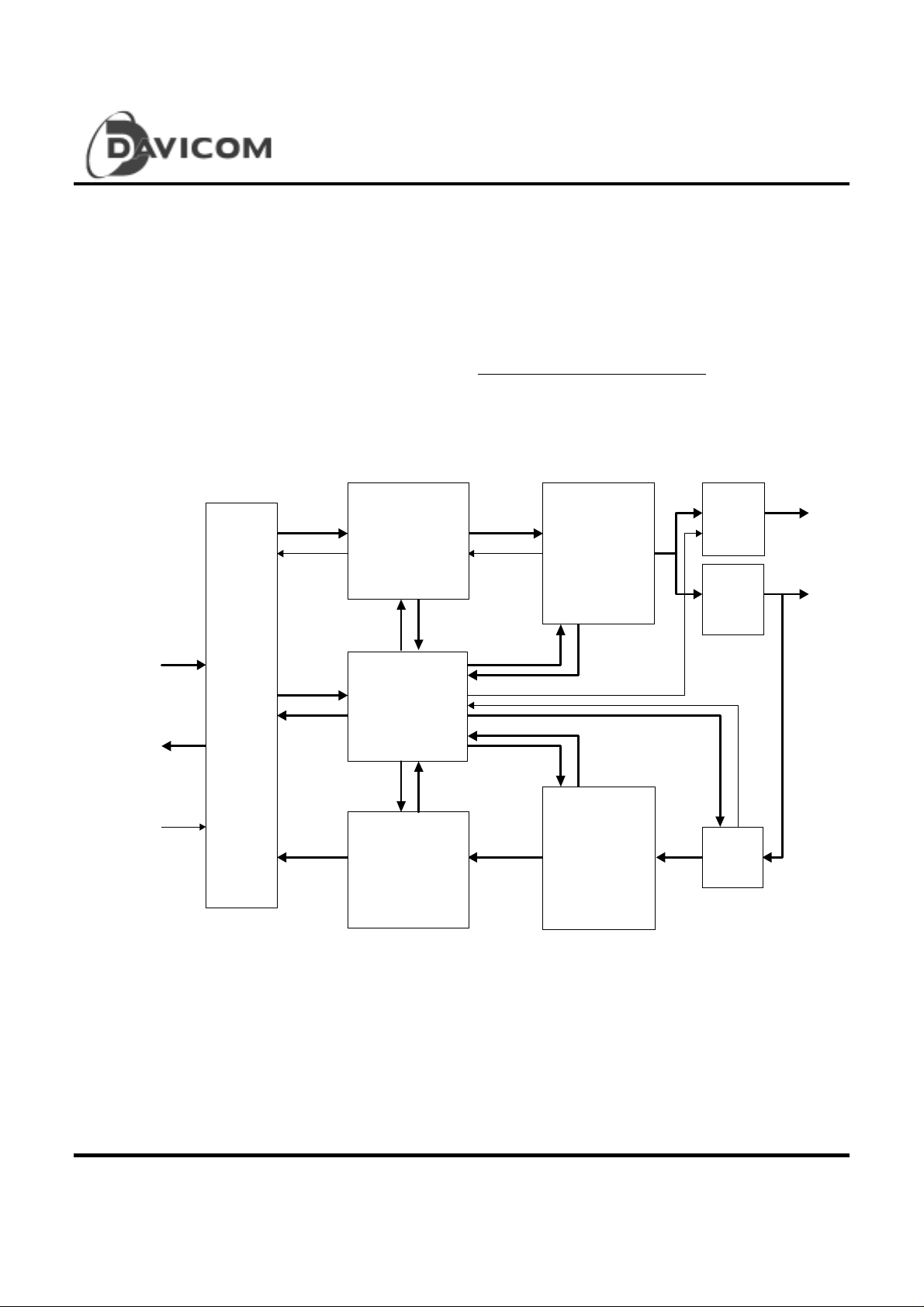
Block Diagram
DM9801
The DM9801 uses a low-power and high-performance
CMOS process. It contains the entire physical layer
functions of 1M as defined by Home Phoneline Network
Alliance, Rev. 1.1, including the Physical Coding
Sublayer, (RLL25) Encoder/Decoder (ENC/DEC), 4-wire
HN Driver circuit and receiver an alog front end (AFE).
Patent-Pending Circuitry Includes:
An enhanced 4-wire Home Network transceiver circuit.
GPSI - MII
Transmit
GPSI - MII
Receive
Interface
Select
Muxed
GPSI
or Mii
Interface
RLL25
Encoder
Master
PHY
Controller
RLL25
Decoder
Transmit
Timing
Generator
Receiever
and
Digital PLL
HN
Secondary
Driver
HN
Primary
Driver
Receiver
AFE
HNB+/-
HNA+/-
Preliminary 1
Version: DM9801-DS-P 02
March 20, 2000

1M Home Phoneli ne Network P hysi cal Layer Si ngle Chi p Transcei ver
Features
DM9801
• 1M Home Phoneline Network physical-layer, single-
chip transceiver
• Supports the MII including the MDIO/MDC serial
management interface
• Supports the GPSI including a SPI serial
management interface
• Supports Link Integrity function
• Smart equalizer circuit for 1M receiver
• Supports Patent Pending 4-wire operation
• Supports hardware or software speed select
• Supports Interrupt on change, eliminates
management polling
• Flexible buil t-in LE D support for TX Activity, RX
Activity and Collision Indication or Activity, Link state
and Collision
• Digital PLL circuit using advanced digital algorithm to
reduce jitter
• Low-power, high-performance CMOS process
• Available in a s mall outline 100- pin LQFP
• 3.3V DC p ow e r w ith 5V DC tol erant I/O
2 Preliminary
Version: DM9801-DS-P 02
March 20, 2000

1M Home Phoneline Netwo rk Physical La yer Si ngle Chip T ranscei ver
Pin Configu ration: DM9801, 100-pin LQFP
RXD1
NC
NC
NC
RXD0(SRXDAT)
RXD3
RXD2
CRS
COL(CLSN)
NC
RX_DV(SO)
RX_CLK(SRDCLK)
TX_CLK(STDCLK)
NC
DGND
TXD0(STXDAT
TXD1(BP1)
TXD3(SMODE)
TX_EN(STXEN)
TXD2(SI)
NC
NC
DGND
DM9801
NC
NC
NC
NC
NC
DVCC
NC
INT#
LNKSTA
PHYAD1
PHYAD2
PHYAD3
COLLED#
RXLED#(LNKLED#)
TXLED#(ACTLED#)
DGND
NC
NC
NC
NC
AVCC
NC
BGREF
BGGND
NC
NC
NC
1
2
3
4
5
6
7
8
9
10
11
12
13
14
15
16
17
18
19
20
21
22
23
24
25
9998979695
100
26
27
29
28
949392
30
3132333435
91
908988
87
DM9801E
3738394041
36
8685848382
44
42
43
8079787776
81
454647
48
49
50
75
74
73
72
71
70
69
68
67
66
65
64
63
62
61
60
59
58
57
56
55
54
53
52
51
NC
NC
NC
DVCC
DVCC
NC
NC
PHYAD0
MDIO(SCS#)
MDC(BP0)
TRIDRV
RESET#
CONFIG0
CONFIG1
INTFSEL
CMDENA
SPDSEL
PWSEL
FWENA
NC
DGND
NC
TSTMODE
NC
NC
NC
NC
AGND
NC
AGND
NC
NC
AVCC
AVCC
NC
HNPA
HNNA
AGND
AGND
HNPB
HNNB
NC
NC
AVCC
XTAL1
XTAL2
NC
DGND
PHYAD4
NC
Preliminary 3
Version: DM9801-DS-P 02
March 20, 2000
1M Home Phoneli ne Network P hysi cal Layer Si ngle Chi p Transcei ver
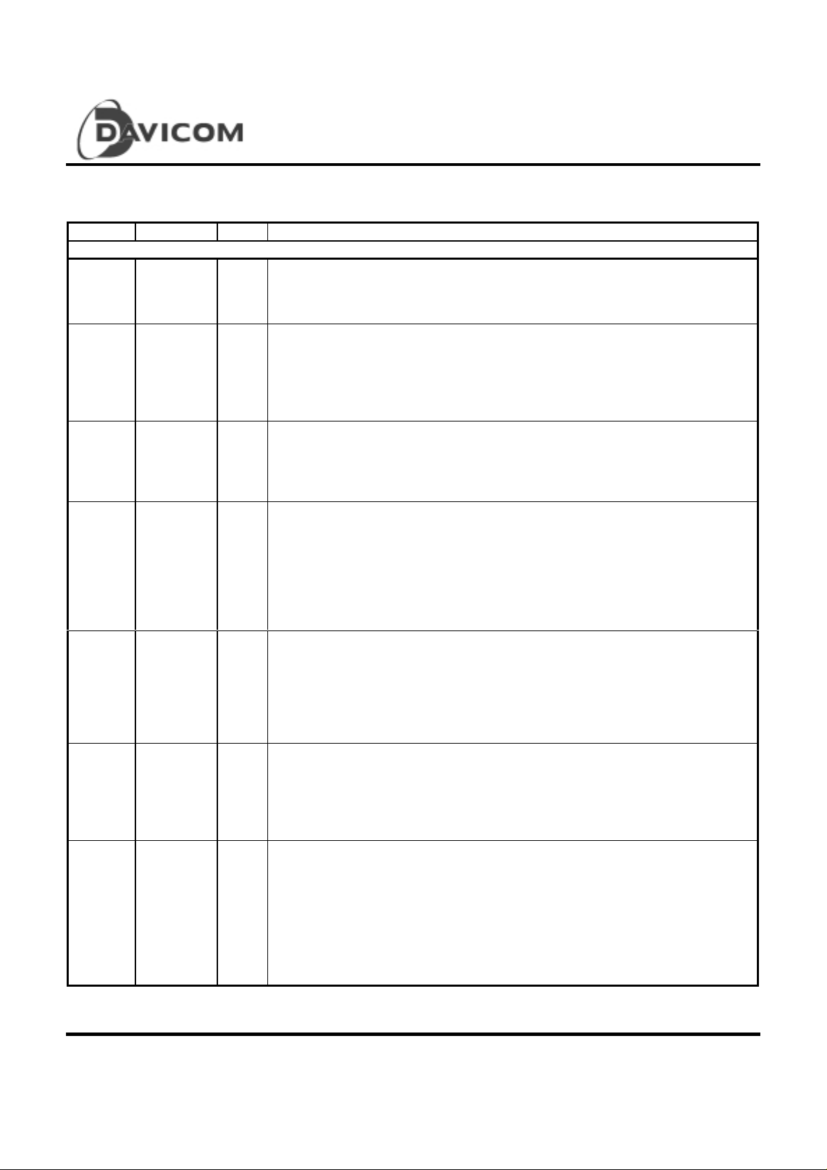
Pin Descr iption
Pin No. Pin Name I/O Description
Station Interface: Receive Data, Transmit Data and Management
85 TXD0
or
STXDAT
84 TXD1
or
BP1
83 TXD2
or
SI
82 TXD3
or
SMODE
86 TX_CLK
or
STDCLK
81 TX_EN
or
STXEN
66 MDC
or
BP0
O,Z
Transmit Data Bit 0 (MII Mode, INTFSEL = 0):
I
Transmit data input pin, bit 0, for nibble data from the MI I
Serial Transmit Data Bit (GPSI Mode, INTFSEL = 1):
Transmit data input pin for serial data from the GPSI.
Transmit Data Bit 1 (MII Mode, INTFSEL = 0):
I
Transmit data input pin, bit 1, for nibble data from the MI I
SPROM Boot Page Select 1 (GPSI Mode, INTFSEL = 1):
Most significant bit of a 2-bit encoded select. The BP1 and BP0 inputs, select
one of four, 64-byte, SPROM pages to initialize the DM9801 management
registers. Master mode must be selected using the SMODE input.
Transmit Data Bit 2 (MII Mode, INTFSEL = 0):
I
Transmit data input pin, bit 2, for nibble data from the MI I
Serial Data Input (GPSI Mode, INTFSEL = 1):
This is the serial data input pin to the DM9801 for the SPI bus. The SPI bus
operation is only valid if GPSI mode is select ed.
Transmit Data Bit 3 (MII Mode, INTFSEL = 0):
I
Transmit data input pin, bit 3, for nibble data from the MI I
Serial Mode Select (GPSI Mode, INTFSEL = 1):
This input pin selects the SPI buses mode of oper ation. The SPI bus modes
of operation are:
Master Mode (SMODE = 0)
Slave Mode (SMODE = 1)
The SPI bus operation is only v alid if GPSI mode is selected.
MII Transmit Clock (MII Mode, INTFSEL = 0):
TX_CLK is an output pin from the DM9801. Used as the transmit data
reference clock, to clock in nibble data from the M I I when in MII interface
mode.
Serial Transmit Data Clock (GPSI Mode, INTFSEL = 1):
STDCLK is an output from the DM9801. Used as the transmit reference clock
to clock in the STXDATA when in GPSI interface mode.
MII Transmit Enable (MII Mode, INTFSEL = 0):
I
MII Transmit enable input, used to enable the transmit function of the MII
when in MII interface mode.
Serial Transmit Enable (GPSI Mode, INTFSEL = 1):
Used to enable the transmit function of the GPSI when in GPSI interface
mode.
MII Serial Management Clock (MII Mode, INTFSEL = 0):
I
Synchronous clock to the MDIO management data input/output serial
interfac e which is asynchronous to transmit and receive clocks. The
maximum clock rate is 2.5MHz.
SPROM Boot Page Select 0 (GPSI Mode, INTFSEL = 1):
Least significant bit of a 2-bit encoded select. The BP1 and BP0 inputs,
select one of four, 64-byte, SPROM pages to initialize the DM 9801
management registers. Master mode must be selected using the SMODE
input.
DM9801
4 Preliminary
Version: DM9801-DS-P 02
March 20, 2000
DM9801
1M Home Phoneline Netwo rk Physical La yer Si ngle Chip T ranscei ver
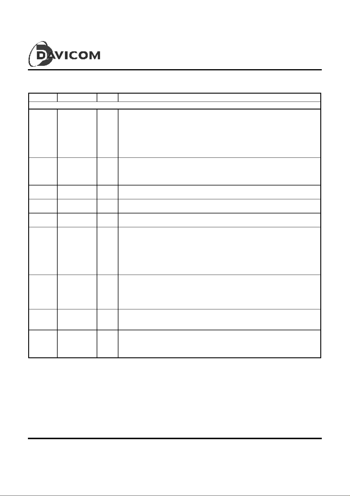
Pin Descr iption
(Continued)
Pin No. Pin Name I/O Description
Station Interface: Receive Data, Transmit Data and Management (Continued)
67 MDIO
Or
SCS#
97 RXD0
Or
SRXDAT
96 RXD1 O,Z
95 RXD2 O,Z
94 RXD3 O,Z
90 RX_CLK
Or
SRDCLK
91 RX_DV
Or
SO
93 CRS O,Z
92 COL
or
CLSN
I/O,Z
O,Z
O,Z
O,Z
O,Z
MII Serial Management Data (MII Mode, INTFSEL = 0):
Bi-directional management instruction/data signal that may be driven by the
station management entity or the PHY. This pin requir es a 1.5KΩ pull-up
resistor.
Serial Interf ace Chip Select (GPSI M od e, INTFSEL = 1):
SCS# is a bi-directional management chip select signal that may be driven
by the station management entity or the PHY. (Active low)
Receive Data Bit 0 (MII Mode, INTFSEL = 0):
Receive data output pin, bit 0, for nibble data to the MII
Serial Receive Data Bit (GPSI Mode, INTFSEL = 1):
Receive data output pin for serial data to the GPSI.
Receive Data Bit 1:
Receive data output pin, bit 1, for nibble data to the
Receive Data Bit 2:
Receive data output pin, bit 2, for nibble data to the MII
Receive Data Bit 3:
Receive data output pin, bit 3, for nibble data to the MII
MII Receive Clock (MII Mode, INTFSEL = 0):
RX_CLK is an output pin from the DM9801. Used as the receive data
reference clock, to clock out nibble data from the MII when in MII interface
mode.
Serial Receive Data Clock (GPSI Mode, INTFSEL = 1):
SRDCLK is an output from th e DM9801. Used as the receive reference
clock to clock out the SRXDATA when in GPSI interface mode.
Receive Data Valid (MII Mode, INTFSEL = 0):
RX_DV is asserted high to indicate that valid data is present on RXD[3:0].
Serial Data Output (GPSI Mode, INTFSEL = 1):
This is the serial data output pin from the DM9801 fo r the SPI bus. The SPI
bus operation is only v alid if GPS I mode i s selected.
Carrier Sense:
This pin is asserted high to indicate the presence of carrier due to receive
or transmit activities.
Collision Detect MII Mode, INTFSEL = 0):
COL is asserted high to indicat e dete ction of collision condition.
Collisi on De tect (GPS I M o de , INTFS E L = 1 ) :
CLSN is asserted high to indicate detection of collision condition.
Preliminary 5
Version: DM9801-DS-P 02
March 20, 2000
DM9801
1M Home Phoneli ne Network P hysi cal Layer Si ngle Chi p Transcei ver
Pin Descr iption
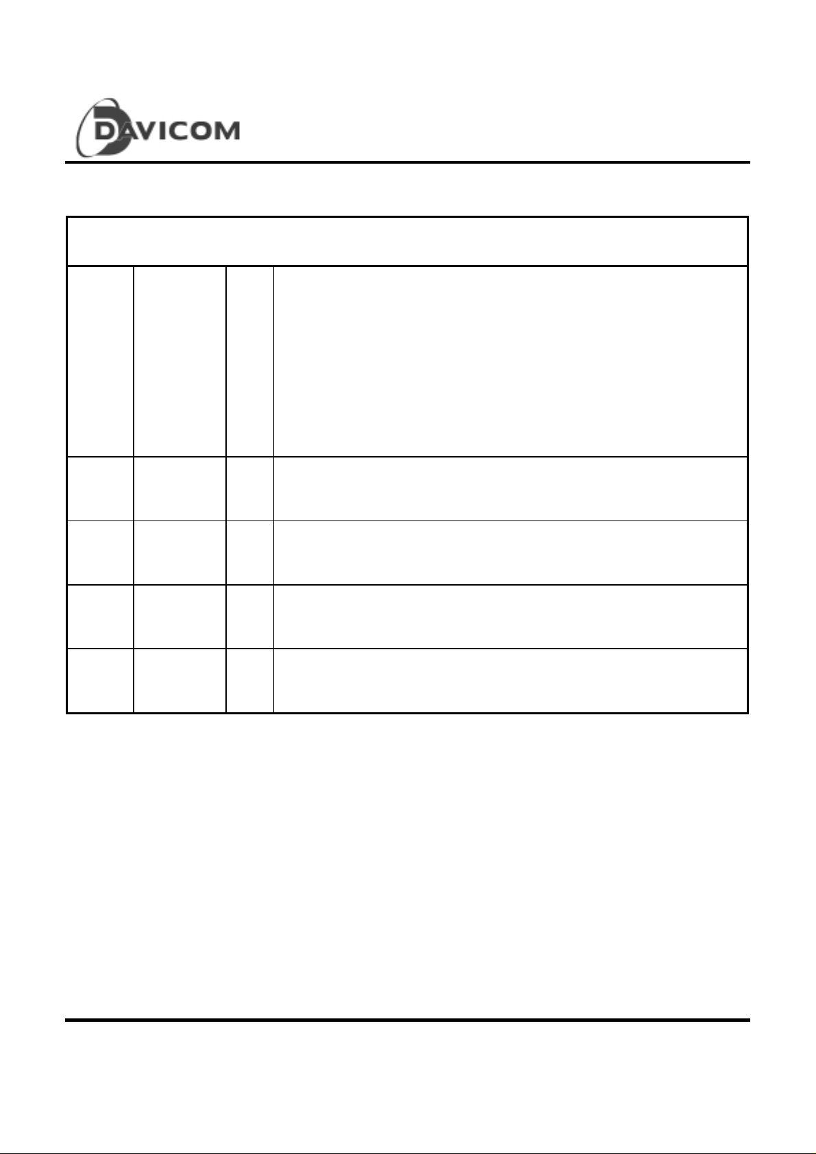
PHY Address Interface:
PHYAD[4:0] provides up to 32 unique PHY address. An address selection of all zeros (00000) will result in a
PHY isolation condition. See the isolate bit description in the BMCR, address 00.
68 PHYADSEL
8 PHYAD1 I/O,
9 PHYAD2 I/O,
10 PHYAD3 I/O,
47 PHYAD4 I/O,
(Continued)
(PHYAD0)
Or
SCLK
I/O,Z
Z
Z
Z
Z
MII Serial Management PHY Address Select (MII Mode, INTFSEL = 0):
PHYADSEL is an input signal that selec ts one of two PHY addresses within
the 32 address range for the DM9801 MII management inter fa ce when both
CONFIG1 and CONFIG0 are not set to 1.
0 = 0x01 address
1 = 0x1F address
PHY Address 0 (MII Mode, INTFSEL = 0):
PHY address bit 0 for mult iple PH Y address applications. Both CONFIG1
and CONFIG0 must be set to 1.
Serial Interface Clock (GPSI Mode, INTFSEL = 1):
SCLK is a bi-directional clock signal used to synchronize SI, SO and SCS#
to and from the DM9801 SPI bus.
PHY Address 1 (MII Mode, INTFSEL = 0):
PHY address bit 1 for mult iple PH Y address applications. Both CONFIG1
and CONFIG0 must be set to 1. Leave unconnected when both CONFIG1
and CONFIG0 are not 1.
PHY Address 2 (MII Mode, INTFSEL = 0):
PHY address bit 2 for mult iple PH Y address applications. Both CONFIG1
and CONFIG0 must be set to 1. Leave unconnected when both CONFIG1
and CONFIG0 are not 1.
PHY Address 3 (MII Mode, INTFSEL = 0):
PHY address bit 3 for mult iple PH Y address applications. Both CONFIG1
and CONFIG0 must be set to 1. Leave unconnected when both CONFIG1
and CONFIG0 are not 1.
PHY Address 4 (MII Mode, INTFSEL = 0):
PHY address bit 4 for mult iple PH Y address applications. Both CONFIG1
and CONFIG0 must be set to 1. Leave unconnected when both CONFIG1
and CONFIG0 are not 1.
6 Preliminary
Version: DM9801-DS-P 02
March 20, 2000
DM9801
1M Home Phoneline Netwo rk Physical La yer Si ngle Chip T ranscei ver
Pin Descr iption
Pin No. Pin Name I/O Description
Configuration and Control Int erf ace:
64 RESET# I
63
62
61 INTFSEL I
60 CMDENA I
59 SPDSEL I
58 PWRSEL I
65 TRIDRV I
57 FWENA I
6INT#OD
(Continued)
CONFIG0
CONFIG1
Reset:
Active Low input that initializes the DM9801. Should remain low for 10ms
after VCC has stabilized at 3.3Vdc (nominal) before it transitions high.
Configuration Select 1:0:
I
These input pins select the DM9801 configuration from a reset condition.
CONFIG1 CONFIG0 Config ur a tion Selecte d
0 0 TXLED, RXLED and COLLED
configuration *
0 1 ACTLED, LNKLED and COLLED
configuration *
1 0 ACTLED, LNKLED and COLLED
configuration with MII Management
Register 0-6 emulation support *
1 1 ACTLED, LNKLED and COLLED
Configuration with MII Management
Register 0-6 e mulation and 32 PHY
addresses support
*see the DM9801 description for a more detailed explanation
Interface Select:
This pin selects either the MII interface or the GPSI interface.
0 = MII
1 = GPSI
Command Enable:
This pin enables a remote m aster node to alter the management register
values of the local DM9801.
Speed Select:
This pin will select the 1M network speed.
0 = Low Speed
1 = High Speed
Power Select:
This pin will sel ec t the 1M network power.
0 = Low Po wer
1 = High Power
Tri-state all Outputs:
This pin, when asserted high, will tri-state all outputs (no effect on opendrain outputs).
Four Wire Interface Enable:
This pin, when asserted high, will enable th e HNP B and HNNB driver pair
for operation. When low, the secondary drivers are powered dow n .
Interrupt Request:
This pin will be asserted low when an interrupt condition exists in the
DM9801.
Preliminary 7
Version: DM9801-DS-P 02
March 20, 2000
DM9801
1M Home Phoneli ne Network P hysi cal Layer Si ngle Chi p Transcei ver
Pin Descr iption
Pin No. Pin Name I/O Description
LED Interface :
These outputs can directly drive LEDs or p r ovide status in formation to a network management device.
13 TXLED#
12 RXLED#
11 COLLED# OD
Home Phoneline Network Media Interface:
36 HNPA ALG
37 HNNA ALG
40 HNPB ALG
41 HNNB ALG
(Continued)
or
ACTLED#
or
LNKLED#
OD
OD
Transmit LED:
Indicates the DM9801 is transmitting data (Active low, Open drain). Config0
= 0 and Config1 = 0
Activity LED:
Indicates the DM9801 is either transmitting or receiving data (Active low,
Open drain).
Receive LED:
Indicates the presence of receive data activity by the DM9801(Active low,
Open drain). Config0 = 0 and Config1 = 0
Link LE D:
Indicates Good Link stat us and that the Link Integrity Timer has not expired
(Active low, Open drain).
Collisi on LE D :
Indicates the presence of collision activity o n the 1M n etwor k (Active l ow,
Open drain).
Home Network Interface, Positive, Primary:
This is the positive interface connection of the primary 1M network
interface.
Home Network Interface, Negative, Primary:
This is the negative interface connection of the primary 1M network
interface.
Home Network Interface, Positive, Secondary:
This is the positive interface connection of the secondary 1M network
interface.
Home Network Interface, Negative, Secondary:
This is the negative interface connection of the secondary 1M network
interface.
8 Preliminary
Version: DM9801-DS-P 02
March 20, 2000
DM9801
1M Home Phoneline Netwo rk Physical La yer Si ngle Chip T ranscei ver
Pin Descr iption
Pin No. Pin Name I/O Description
Miscellaneous:
7 LNKSTA I/O,Z
45 XTAL1 ALG
46 XTAL2 ALG
21 BGREF ALG
22 BGGND ALG
53 TSTMODE I
1, 2,
3,5,
15 – 18,
20,
23 – 27,
30 - 32,
35, 42,
44,
49 – 52,
54, 56,
69, 70,
73 – 78,
80, 87,
89, 98,
99, 100
Power and Ground:
The power (VCC) and ground (GND) pins of the DM9801 are grouped in pairs of two categories - Digital
Circuitry Power/Ground Pairs and Analog Circuitry Power/Ground Pair.
14, 48,
55, 79,
88,
4, 7 1 , 7 2 DVCC P Digital logic power supply
28, 29,
38, 39
19, 33,
34, 43
(Continued)
Link Sta tus:
Output, positive true logic. Indication of Link Status.
Crystal Pin 1:
This pin should be connected to one side of a 20MHz (±50 ppm) cr y stal.
Crystal Pin 2:
This pin should be connected to the other side of a 20MHz (±50 ppm)
crystal.
Bandgap Voltage Reference:
Connect a 6.20_KΩ, 1% resistor between this pin and the BGGND pin to
provide an accurate current reference for the DM9801.
Bandga p Voltage R eferenc e Retur n:
Return pin for the 6.20_KΩ resistor connection.
Test Mode Control Pin:
TSTMODE=0: Normal operating mode.
TSTMODE=1: Enable test mode.
NC
DGND P Digital logic ground
AGND P Analog circuit ground
AVCC P Analog circuit power supply
No Connect:
These pins are reserved. Leave these pins unconnected ( floating ).
Preliminary 9
Version: DM9801-DS-P 02
March 20, 2000
DM9801
1M Home Phoneli ne Network P hysi cal Layer Si ngle Chi p Transcei ver
Functional D escrip tion
The DM9801 is a single-chip Home Phoneline Network
transceiver .The DM9801 pr ovides an IEEE 802.3u
subset Media Independent Interface (MII) or a pseudostandard General Purpose Serial Interface (GPSI).
Encoder
Muxed
GPSI or MII
Interface
Master PHY
Controller
Decoder
RLL25
RLL25
The DM9801 enables home networking by allowing
Ethernet packets to be transported over common home
telephone wiring with no modifications, using Ethernet
CSMA/CD media access control procedures as defined in
the IEEE 802.3 standard. Figure 1 sho ws the major
functional blocks implemented in the DM9801.
Transmit
Timing
Generator
HN Drivers
Receiver AFE
Receiver
and
Digital PLL
Figure 1
MII Interface
The DM9801 provides a subset Media Independent
Interface (MII) or a pseudo-standard General Purpose
Serial Interface (GPSI). The MII interface provides a
simple, easy way to implement connection between the
MAC Reconciliation layer and the DM9801 transceiver.
The MII is designed to make the differences between
various media transparent to the MAC sublayer.
The MII consists of a nibble wide receive data bus, a
nibble wide transmit data bus, and control signals to
facilitate data transfers between the PHY and the
Reconciliation layer.
10 Preliminary
TXD (transmit data) is a nibble (4 bits) of da ta that are
driven by the reconciliation sublayer synchronously with
respect to TX_CLK. For each TX_CLK period, which
TX_EN is asserted, TXD (3:0) are accepted for
transmission by the PHY.
TX_CLK (trans mit clock) o utput to the MAC r econciliatio n
sublayer is a clock that provides the timing reference for
the transfer of the TX_EN, TXD, and TX_ER signals.
TX_EN (transmit enable) input from the MAC
reconciliation sublayer to indicate nibbles are being
presented on the MII for transmission on the physical
medium.
Version: DM9801-DS-P 02
March 20, 2000

1M Home Phoneline Netwo rk Physical La yer Si ngle Chip T ranscei ver
MII Interface (continued)
RXD (receive data) is a nibble (4 b its) of data that are
sampled by the reconciliation sublayer synchronously with
respect to RX_CLK. For each RX_CLK period that
RX_DV is asserted, RXD (3:0) are transferred from the
PHY to the MAC reconciliation sublayer.
RX_ CL K ( re cei ve clo ck ) o u tp ut t o t he MAC re co n cili a tio n
sublayer is a clock that provides the timing reference for
the transfer of the RX_DV, RXD, and RX_ER signals.
RX_DV (receive data v alid) input from the PHY to indicate
the PHY is presenting recovered and decoded nibbles to
the MAC reconciliation sublayer. To interpret a receive
frame correctly by the reconciliation sublayer, RX _DV
must encompass the frame starting no later than the Startof-Frame delimiter and excluding any End-Stream
delimiter.
DM9801
The DM9801 management functions correspond to
MII specification for IEEE 802.3u-1995 (Clause 22)
for registers 0 through 6 with vendor-specific
registers 16 through 31.
In read/write operation, the management data frame
is 64-bits l ong and starts with 32 contiguous l o gi c
one bits (preamble) synchronization clock cycles on
MDC. The Start of Fram e Delimiter (SFD) is
indicated by a <01> pattern followed by the
operation code (OP):<10> indicates Read operation
and <01> indicates Write operation. For read
operation, a 2-bit turnaround (TA) filin g between
Register Address field and Data field is provided for
MDIO to avoid contention. Following the turnaround
time, 16-bit data is read from or written to the
management regi ster s.
CRS ( ca rr ie r s e ns e) is as s ert ed by t h e PH Y when ei t her
the transmit or receive medium is non-idle and deasserted
by the PHY when the transmit and receive medium are
idle .
MII Ser ia l Management
The MII serial management interface consists of a
data interface, basic register set, and a serial
management interface to the register set. Through
this interface it is possible to control and configure
multiple PHY devices, get status and error
information, and determine the type and capabilities
of the attached PHY device(s).
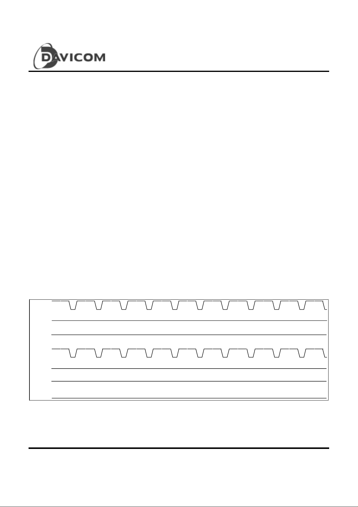
MII Inte rfa ce Transmi t and Re c eive Timing Diagram
TX_CLK
TX_EN
TXD
RX_CLK
CRS
Serial Management Interface
The serial control interface uses a simple two-wired
serial interface to obtain and control the status of
the physical layer through the MII interface. The
serial control interface consists of MDC
(Management Data Clock), and MDI/O
(Management Data Input/Output) signals.
The MDIO pin is bi-directional and may be shared
by up to 32 devices.
0
RXD
RX_DV
COL
0
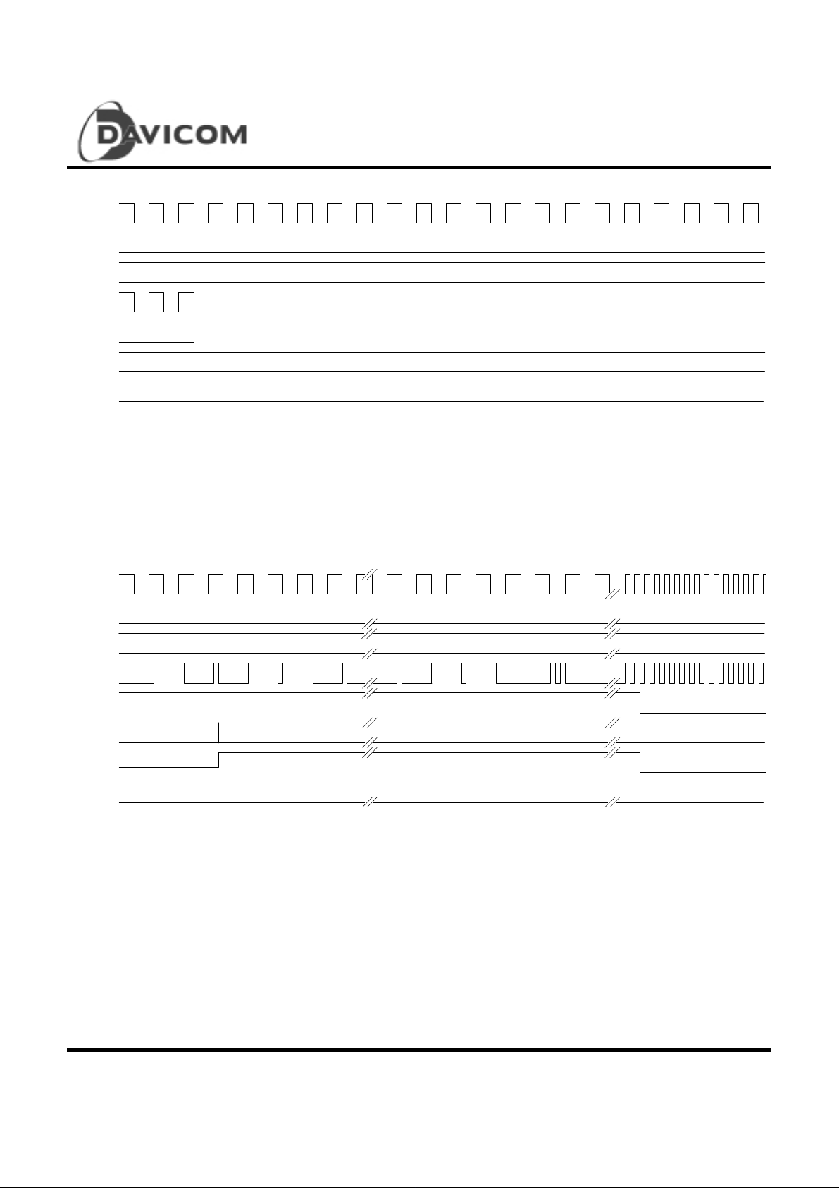
RX_CLK and TX_CLK are synchronized. All signals are inactive. The period of the two clock is 2333.3 ns.
Idle S tate
Figure 2
Preliminary 11
Version: DM9801-DS-P 02
March 20, 2000
1M Home Phoneli ne Network P hysi cal Layer Si ngle Chi p Transcei ver
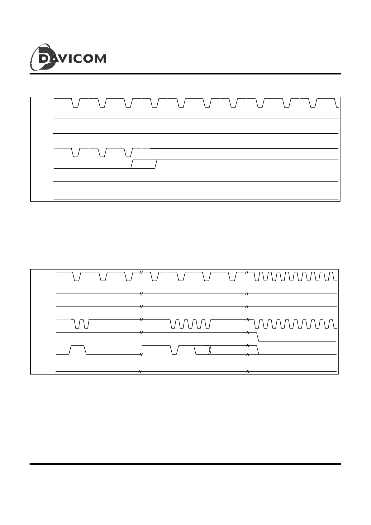
MII Inte rfa ce Transmi t and Re c eive Timing Diagram (continued)
TX_CLK
TX_EN
DM9801
TXD
RX_CLK
CRS
RXD
RX_DV
COL
0
0
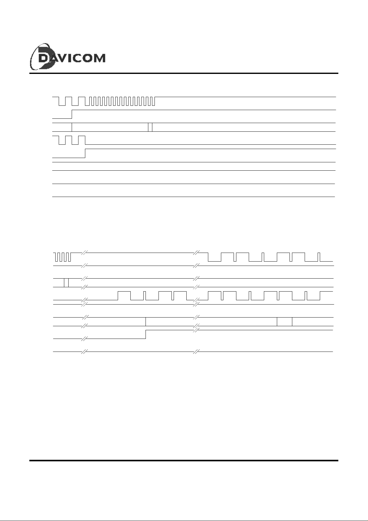
RX_CLK becomes disabled (and left in the low state) as soon as CRS is asserted. The clock is re-enabled about 140 u S into
the pac k et.
RXPKT – CRS Asserted
Figure 3
TX_CLK
TX_EN
TXD
RX_CLK
000
CRS
RXD
RX_DV
COL
0
5 (Pream bl e)
DATA 0
RX_CLK and TX_CLK are unrelated to each other during this time. When a symbol has been received and decoded,
RX_CLK toggles at various frequencies depending on what data have been received. Once CRS falls, RX_CLK and
TX_CLK are toggled continuously at 933.3 ns for 22 cycles, after which DM9801 returns to the Idle State.
RXPKT – RX_CLK Active and CRS Cleared
Figure 4
12 Preliminary
Version: DM9801-DS-P 02
March 20, 2000
1M Home Phoneline Netwo rk Physical La yer Si ngle Chip T ranscei ver
MII Inte rfa ce Transmi t and Re c eive Timing Diagram (continued)
TX_CLK
TX_EN
DM9801
TXD
RX_CLK
CRS
RXD
RX_DV
COL
0
5 (Pream bl e)
D
0
DATA
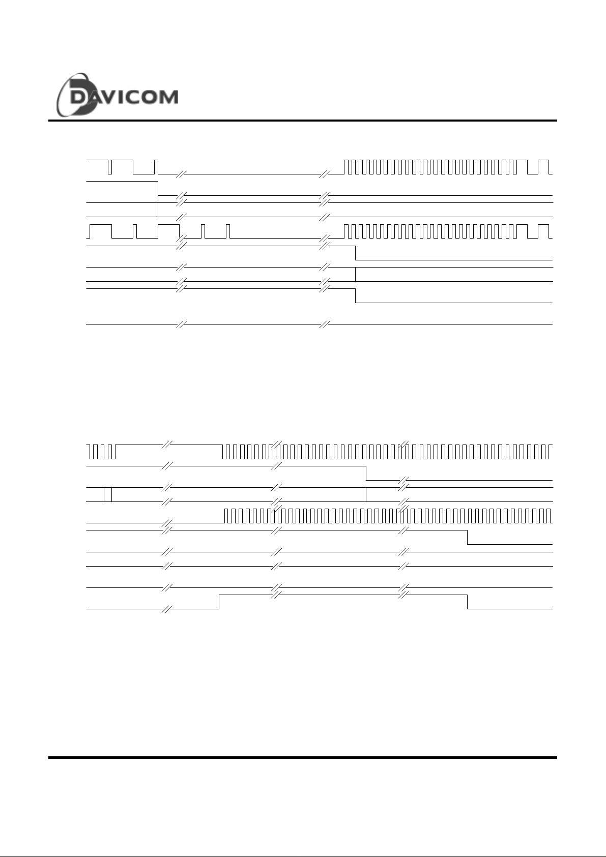
Once TX_EN is asserted, DM9801 stops RX_CLK, asserts CRS, and toggles TX_CLK at 933.3 ns.
TXPKT – TX_EN Asserted
Figure 5
TX_CLK
TX_EN
D DATA
TXD
RX_CLK
5
CRS
RXD
RX_DV
COL
0
5 (Preambl e)
D
DATA
TX_CLK continues to toggle at 933.3 n s until t he SF D is observed, as shown in the first section of the above diagram. At this
point, TX_CLK is disabled (high) until AID header has been transmitted on the wire (or until a COL has been detected). This
takes about 120 us, at which time RX_CLK starts toggling, thereby shifting 32 bits of preamble and SF D ba ck to t he M AC.
Sometime later, the TX_CLK restarts a s symbols get sent onto the wire in an analogous manner as RX_CLK during packet
reception.
TXPKT – R X_C LK A ct ive
Figure 6
Preliminary 13
Version: DM9801-DS-P 02
March 20, 2000
1M Home Phoneli ne Network P hysi cal Layer Si ngle Chi p Transcei ver
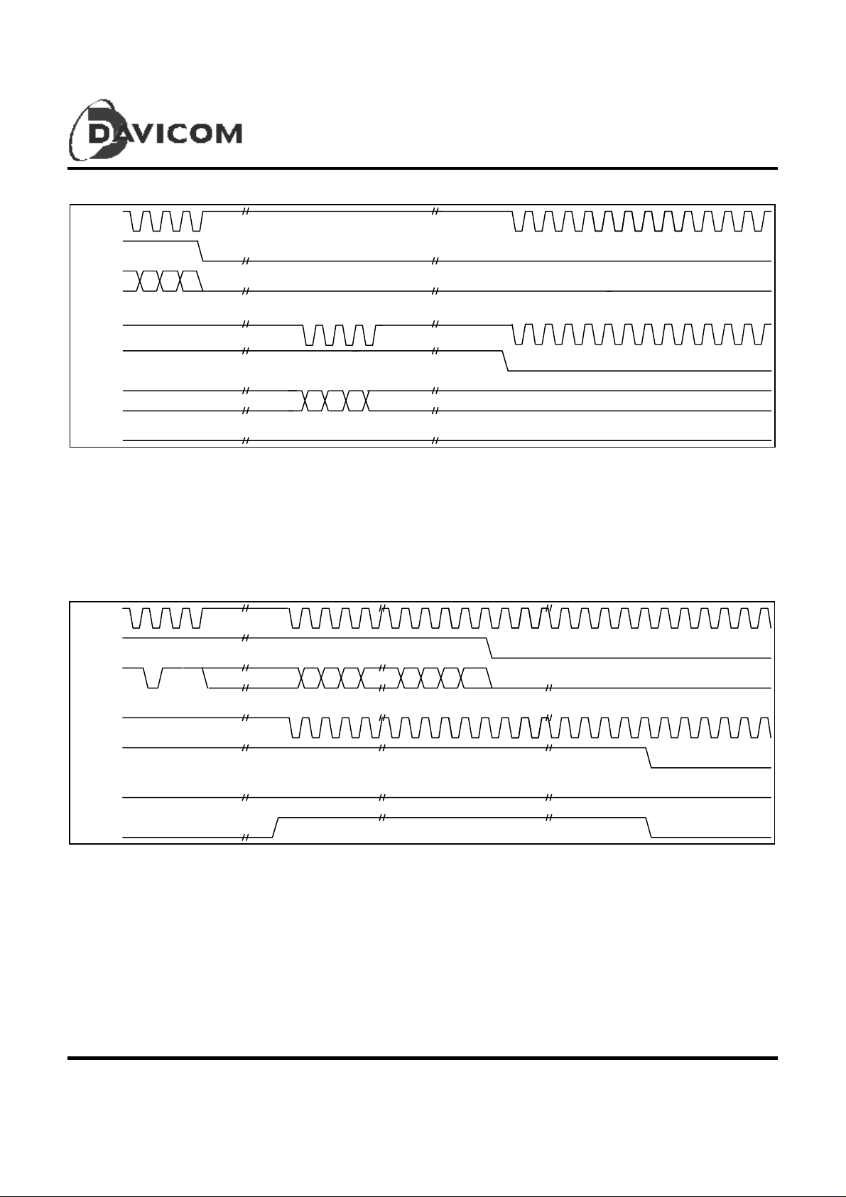
MII Inte rfa ce Transmi t and Re c eive Timing Diagram (continued)
TX_CLK
TX_EN
DM9801
TXD
RX_CLK
CRS
RXD
RX_DV
COL
DATA
DATA
0
0
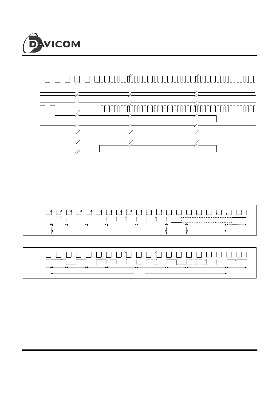
Once TX_EN is cleared, the last symbol gets encoded and tr an sm itt ed , th e looped-back data is presented back to the MAC,
and CRS falls. Once CRS falls, TX_CLK and RX_CLK toggles with a period of 933.3 ns for 22 c locks, after which the system
returns to the Idle S tate .
TXPKT – TX_EN Cleared
Figure 7
TX_CLK
TX_EN
D DATA 0
TXD
5
RX_CLK
CRS
RXD
RX_DV
COL
0
0
COL will be asserted sometime after the preamble and SFD have been clocked in. TX_CLK and RX_CLK are then clocked
with a period 933.3 ns until CRS d rops. TX_EN drops sometime after COL was asserted. CRS and COL are dropped after
more tha n 80 cloc ks . TX_C LK and RX _CLK keep togg ling at 933. 3 ns period for roughly another 25 clock cycles, when the
system returns to the Idle State.
TXPKT – COL Asserted
Figure 8
14 Preliminary
Version: DM9801-DS-P 02
March 20, 2000
1M Home Phoneline Netwo rk Physical La yer Si ngle Chip T ranscei ver
MII Inte rfa ce Transmi t and Re c eive Timing Diagram (continued)
TX_CLK
TX_EN
DM9801
TXD
RX_CLK
CRS
RXD
RX_DV
COL
0
00
0
COL may be asserted up to 120 us after CRS has been asserted. Once COL has been asserted, TX_CLK and RX_CLK run
at a period of 933.3 ns until COL and CRS are cleared. It can take up to about 600 us for CRS to clear.
RXPKT – COL Asserted
Figure 9
Management Interface - Read Frame Structure
MDC
MDIO Read
32 "1"s
Idle Preamble SFD Op Code PHY Address Register Address Turn Around Data Idle
0110A4A3A0R4R3R0
Write
Z
0
D15 D14 D1 D0
//
Read
//
Management Interface - Write Frame Structure
MDC
MDIO Write
32 "1"s 0 1 10 A4 A3 A0 R4 R3 R0 1 0 D15 D14 D1 D0
Idle Preamble SFD Op Code PHY Address Register Address Turn Around Data Idle
Write
Figure 10
Preliminary 15
Version: DM9801-DS-P 02
March 20, 2000
1M Home Phoneli ne Network P hysi cal Layer Si ngle Chi p Transcei ver
General Purpose Serial Interface
The DM 9801 provides a subset Media Independent
Interface (MII) or a pseudo-standard General Purpose
Serial In te rface ( GPS I). The GPS I inte r face pr o vides a
simple, easy way to implement connection between the
MAC Reconciliation layer and the DM9801 transceiver.
The GPSI is designed to make the differences between
various media transparent to the MAC sublayer.
The GPSI interface provides a serial receive d ata bus, a
seria l trans mit dat a bu s, a nd control signals to faci litate
data transfers between the DM9801 transceiver and the
Reconciliation layer. The seven signals which comprise
the GPSI are STXDAT, STDCLK, STXEN, SRXDAT,
SRXCLK, CLSN, and CRS. Of these, only STXEN and
STXDAT are inputs to the DM9801, the other five are
outputs from the DM9801.
DM9801
STXEN (serial transmit enable) input from the MAC
reconciliation sublayer to indicate serial data is being
prese nted on the GPSI for transmissio n o n the phy sical
medium.
SRXDAT (serial receive data) is a serial stream of data
that is sampled by the reconciliation s ublayer
synchronously with respect to SRXCLK.
SRXCLK (serial receive data clock) is an output to the
MAC reconciliation sublayer. SRDCLK is a clock that
provides the timing reference for the transfer of the
SRXDAT in GPSI mode.
CLSN (c ol lision dete ct) is an o utput to t he MAC
re c o n c il ia tio n su b layer. CLSN is asserted high to
indicate detection of collision condition
STXDAT (serial transmit data) is a serial stream of data
that are driven by the reconciliation sublayer
synchronously with respect to STDCLK. For each
STDCLK period, which STXEN is asserted, STXDAT is
accepted for transmission by the PHY.
STDCLK (s er ial tran s mit d a ta c loc k) is a n o utput to the
MAC reconciliation sublayer. STDCLK is a clock that
provides the timing reference for the transfer of the
STXDAT in GPSI mode.
STDCLK
STXEN
STXDAT
SRDCLK
CRS
CRS (carrier sense) is an output to the MAC reconciliation
sub layer that is asserted high to indicate the
presence of carrier due to receive or transmit
activities.
The subsequent sections analyze each GPSI related state
of the DM9801 in detail.
SRXDAT
CLSN
SRDCLK and STDCLK are synchronized. All other signals are inactive.
Idle S tate
Figure 11
16 Preliminary
Version: DM9801-DS-P 02
March 20, 2000
1M Home Phoneline Netwo rk Physical La yer Si ngle Chip T ranscei ver
General Purpose Serial Interface (continued)
STDCLK
STXEN
STXDAT
SRDCLK
CRS
SRXDAT
CLSN
SRDCLK becomes disabled as soon as CRS is asserted.
RXPKT- CRS Asserted
DM9801
Figure 12
STDCLK
STXEN
STXDAT
SRDCLK
CRS
SRXDAT
CLSN
SRDCLK and STDCLK are unrelated to each other during this time. When a symbol has been received and decoded,
SRDCLK toggles in order to shift out the three to six bits encoded in the symbol. The middle portion of this diagram shows the
end of the preamble, followed by the SFD and the beginning of the datagram. CRS will fall a fter the last received symbol.
Once CRS falls, SRDCLK and STDCLK are toggled continuously for 97 cycles after which the DM9801 returns to the Idle
state.
RXPKT - SRDCLK Active and CRS Cleared
Figure 13
Preliminary 17
Version: DM9801-DS-P 02
March 20, 2000
DM9801
1M Home Phoneli ne Network P hysi cal Layer Si ngle Chi p Transcei ver
General Purpose Serial Interface (continued)
STDCLK
STXEN
STXDAT
SRDCLK
CRS
SRXDAT
CLSN
Once STXEN is asserted, the DM9801 stops SRDCLK, asserts CRS, and toggles STDCLK.
TXPKT - STXEN Asserted
Figure 14
STDCLK
STXEN
STXDAT
SRDCLK
CRS
SRXDAT
CLSN
STDCLK continues to toggle until SFD is observed, as shown in the first section on the abo ve diagram. At this point, STDCLK
is disabled until the AID header has been transmitted on the wire or until CLS has been de tect e d . At th is tim e SRDCLK starts
toggling, thereby shifting 32 bits of preamble and SFD back to the MAC. Sometime later, the STDCLK restarts as symbols get
sent onto the wire in an analogous manner as SRDCLK during packet reception.
TXPKT - SR DCLK Ac tive
Figure 15
18 Preliminary
Version: DM9801-DS-P 02
March 20, 2000
DM9801
1M Home Phoneline Netwo rk Physical La yer Si ngle Chip T ranscei ver
General Purpose Serial Interface (continued)
STDCLK
STXEN
STXDAT
SRDCLK
CRS
SRXDAT
CLSN
Once STXEN is cleared, the last symbol gets encoded and transmitted. The looped-back data is presented back to the MAC
and sometime later CRS falls. Once CRS falls, STDCLK and SRDCLK toggl e for 97 clocks after which the sy stem return s to
the Idle state.
TXPKT - STXEN Cleared
Figure 16
STDCLK
STXEN
STXDAT
SRDCLK
CRS
SRXDAT
CLSN
CLSN will be asserted some time after the preamble and SFD ha ve been clock ed in. STDCLK and SRDCLK are then clocked
until CRS drops. STXEN drops s ometime after CLSN was as serted. CRS and CLSN are dropped togeth er after more than
500 clocks. STDCLK and SRDCLK keep toggling for approximately another 100 clock cycles, then the system returns to the
idle sta te .
TXPKT - CLSN Asserted
Figure 17
Preliminary 19
Version: DM9801-DS-P 02
March 20, 2000
 Loading...