


DM9101
10/100Mbps Ethernet Physical Layer Single Chip Transceiver
General Description
The DM9101 is a physical-layer, single-chip, low-power transceiver for 100Base-TX, and 10Base-T operations. On the media side, it provides a direct interface either to Unshielded Twisted Pair Category 5 Cable (UTP5) for 100Base-TX Fast Ethernet, or UTP5/UTP3 Cable for 10Base-T Ethernet. Through the IEEE 802.3u Media Independent Interface (MII), the DM9101 connects to the Medium Access Control (MAC) layer, ensuring a high interoperability among products from different vendors.
Sublayer (PCS), Physical Medium Attachment (PMA), 100Base-TX Twisted Pair Physical Medium Dependent Sublayer (TP-PMD), and a 10Base-T Encoder/Decoder (ENC/DEC). The DM9101 provides strong support for the Auto-negotiation function utilizing automatic media speed and protocol selection. The DM9101 incorporates an internal wave-shaping filter to control rise/fall time, eliminating the need for external filtering on the 10/100Mbps signals.
Patent-Pending Circuitry Includes:
The DM9101 uses a low-power and high-performance CMOS process. It contains the entire physical layer functions of 100Base-TX as defined by IEEE 802.3u, including the Physical Coding
Smart adaptive receiver equalizer
Digital algorithm for high frequency clock/data recovery circuit
High speed wave-shaping circuit
Block Diagram
|
|
|
|
25M OSCI |
|
|
|
LED1-4# |
|
|
|
|
|
|
|
TX CGM |
|
|
|
LED |
|
|
|
|
|
|
|
|
|
|
Driver |
|
|
|
|
|
|
|
|
|
|
|
|
|
|
|
|
|
|
4B/5B |
|
Parallel |
NRZ |
NRZI to |
MLT-3 |
|
|
|
|
|
|
Scrambler |
to |
|
|
100TXD+/- |
|||||
|
|
Encoder |
to Serial |
MLT-3 |
Driver |
|
|
||||
|
|
|
NRZI |
|
|
|
|||||
|
|
|
|
|
|
|
|
|
|
|
|
|
|
|
|
|
|
|
|
Rise/Fall |
|
|
|
|
|
|
|
|
|
|
|
Time |
|
|
|
|
|
|
|
|
|
|
|
CTL |
|
|
|
|
|
|
|
|
25M CLK |
|
|
|
|
|
|
|
|
|
|
|
|
|
125M CLK |
|
|
|
|
MII |
MII |
|
|
|
|
|
|
|
|
|
|
Interface/ |
|
|
|
|
|
|
|
|
|
|
|
Signals |
|
|
|
|
|
|
|
|
|
|
|
Control |
|
Code- |
|
|
|
NRZI |
|
|
|
|
|
|
4B/5B |
|
Serial to |
|
MLT-3 to |
Adaptive |
|
||||
|
|
group |
Descrambler |
|
to |
RXI+/- |
|||||
|
|
Decoder |
Parallel |
|
NRZI |
|
EQ |
||||
|
|
Alignment |
|
|
NRZ |
|
|
||||
|
|
|
|
|
|
|
|
|
|
||
|
|
|
|
|
|
|
|
RX |
|
|
|
|
|
|
|
|
|
|
|
C R M |
|
|
|
|
|
|
|
|
Digital |
|
|
|
|
|
|
|
|
|
|
|
Logic |
|
|
|
|
|
|
|
|
|
|
|
|
|
|
10BASE-T |
RX |
|
RXI+/- |
|
|
|
|
|
|
|
|
|
|
|
|
|
|
|
|
|
|
|
|
Module |
TX |
|
10TXD+/- |
|
|
|
|
|
|
|
|
|
|
||
|
|
|
Register |
Collision |
Carrier |
|
Auto- |
|
|
|
|
|
|
|
|
Detection |
Sense |
|
Negotiation |
|
|
|
|
Final |
|
|
|
|
|
|
|
|
|
|
1 |
Version: DM9101-DS-F03 |
|
|
|
|
|
|
|
|
|
|
|
July 22, 1999 |
|
|
|
|
|
|
|
|
|
|
|

DM9101
10/100Mbps Ethernet Physical Layer Single Chip Transceiver
Table of Contents
General Description ................................................ |
1 |
Block Diagram ........................................................ |
1 |
Features ................................................................. |
3 |
Pin Configuration: DM9101E LQFP......................... |
3 |
Pin Configuration: DM9101F QFP........................... |
4 |
Pin Description ....................................................... |
5 |
Functional Description |
|
MII Interface ...................................................... |
12 |
100Base-TX Operation ...................................... |
14 |
100Base-TX Transmit........................................ |
14 |
100Base-TX Operation ...................................... |
15 |
4B5B Encoder ................................................... |
15 |
Scrambler.......................................................... |
15 |
Parallel to Serial Converter ................................ |
15 |
NRZ to NRZI Encoder........................................ |
15 |
MLT-3 Converter ............................................... |
15 |
MLT-3 Driver ..................................................... |
15 |
4B5B Code Group ............................................. |
16 |
100Base-TX Receiver........................................ |
17 |
Signal Detect ..................................................... |
17 |
Digital Adaptive Equalization.............................. |
17 |
MLT-3 to NRZI Decoder..................................... |
17 |
Clock Recovery Module ..................................... |
18 |
NRZI to NRZ ..................................................... |
18 |
Serial to Parallel ................................................ |
18 |
Descrambler...................................................... |
18 |
Code Group Alignment ...................................... |
18 |
4B5B Decoder ................................................... |
18 |
10Base-T Operation .......................................... |
18 |
Collision Detection............................................. |
18 |
Carrier Sense .................................................... |
18 |
Auto-Negotiation................................................ |
18 |
MII Serial Management...................................... |
19 |
Serial Management Interface ............................. |
19 |
Management Interface – Read Frame Structure.19
Management Interface – Write Frame Structure.19
Register Description ............................................. |
20 |
- Key To Default.................................................... |
20 |
Basic Mode Control Register (BMCR) |
|
- Register 0........................................................... |
21 |
Basic Mode Status Register (BMSR) |
|
- Register 1........................................................... |
22 |
- Register 2 .......................................................... |
23 |
PHY ID Identifier Register #2 (PHYIDR2) |
|
- Register 3 .......................................................... |
24 |
Auto-negotiation Advertisement Register (ANAR) |
|
- Register 4 .......................................................... |
24 |
Auto-negotiation Link Partner Ability Register |
|
(ANLPAR) - Register 5 ......................................... |
25 |
Auto-negotiation Expansion Register (ANER) |
|
- Register 6 .......................................................... |
26 |
DAVICOM Specified Configuration Register (DSCR) |
|
- Register 16......................................................... |
26 |
DAVICOM Specified Configuration and Status |
|
Register (DSCSR) - Register 17 ........................... |
28 |
10Base-T Configuration / Status (10BTSCRCSR) |
|
- Register 18......................................................... |
29 |
Absolute Maximum Ratings .................................. |
30 |
DC Electrical Characteristics ................................ |
31 |
AC Characteristics................................................ |
32 |
Timing Waveforms |
|
MII-100Base-TX Transmit Timing Diagram ........ |
33 |
MII-100Base-TX Receive Timing Diagram ......... |
33 |
Auto-negotiation and Fast Link Pulse Timing ..... |
34 |
MII-10Base-T Transmit Timing Diagram ............ |
35 |
MII-10Base-T Receive Nibble Timing Diagram .. |
35 |
10BASE-T SQE (Heartbeat) Timing Diagram..... |
36 |
10BASE-T Jab and Unjab Timing Diagram ........ |
36 |
MDIO Timing when OUTPUT by STA ................ |
37 |
MDIO Timing when OUTPUT by DM9101.......... |
37 |
Magnetics Selection Guide ................................... |
38 |
Crystal Selection Guide ........................................ |
38 |
Application Circuit (for reference only) .................. |
40 |
Package Information............................................. |
41 |
Ordering Information............................................. |
42 |
Company Overview .............................................. |
42 |
PHY ID Identifier Register #1 (PHYIDR1) |
Contact Windows.................................................. |
42 |
2 Final
Version: DM9101-DS-F03
July 22, 1999
DM9101
10/100Mbps Ethernet Physical Layer Single Chip Transceiver
Features
•10/100Base-TX physical-layer, single-chip transceiver
•Compliant with IEEE 802.3u 100Base-TX standard
•Compliant with ANSI X3T12 TP-PMD 1995 standard
•Compliant with IEEE 802.3u Auto-negotiation protocol for automatic link type selection
•Supports the MII with serial management interface
•Supports Full Duplex operation for 10 and 100Mbps
•High performance 100Mbps clock generator and data recovery circuitry
•Adaptive equalization circuitry for 100Mbps receiver
•Controlled output edge rates in 100Mbps
•Supports a 10Base-T interface without the need for an external filter
•Provides Loop-back mode for system diagnostics
•Includes Flexible LED configuration capability
•Digital clock recovery circuit using advanced digital algorithm to reduce jitter
•Low-power, high-performance CMOS process
•Available in both a 100 pin LQFP and a 100 QFP package
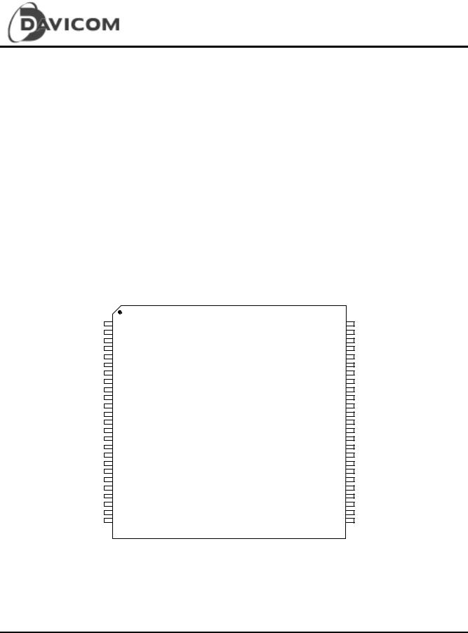
Pin Configuration: DM9101E LQFP
N C |
|
A V C C A G N D A G N D 1 0 B T S E R B P S C R B P 4 B 5 B B P A L I G N R P T R / N O D E # O P M O D E 3 O P M O D E 2 O P M O D E 1 O P M O D E 0 P H Y A D 4 P H Y A D 3 |
|
D V C C D G N D P H Y A D 2 P H Y A D 1 P H Y A D 0 T E S T M O D E R E S E T # R X _ E N R X _ E R / R X D 4 R X _ D V |
||||||||||||||||||||||||||||||||||||||||||||
|
|
|
|
|
|
|
|
|
|
|
|
|
|
|
|
|
|
|
|
|
|
|
|
|
|
|
|
|
|
|
|
|
|
|
|
|
|
|
|
|
|
|
|
|
|
|
|
|
|
|
|
|
|
|
|
|
|
|
|
|
|
|
|
|
|
|
|
|
|
|
|
|
|
|
|
|
|
|
|
|
|
|
|
|
|
|
|
|
|
|
|
|
|
|
|
|
|
0 0 9 9 9 8 9 7 9 6 9 5 9 4 |
9 3 9 2 |
9 1 9 0 8 9 8 8 8 7 8 6 8 5 8 4 8 3 8 2 8 1 8 0 |
7 9 7 8 |
7 7 7 6 |
||||||||||||||||||||||||||||||||||||||||||||
1 |
|
|
|
|
|
|
|
|
|
|
|
|
|
|
|
|
|
|
|
|
|
|
|
|
|
|
|
|
|
|
|
|
|
|
|
|
|
|
|
|
|
|
|
|
|
|
|
|
N C |
1 |
|
|
|
|
|
|
|
|
|
|
|
|
|
|
|
|
|
|
|
|
|
|
|
|
|
|
|
|
|
|
|
|
|
|
|
|
|
|
|
|
|
|
|
|
|
|
|
|
75 |
|
N C |
2 |
|
|
|
|
|
|
|
|
|
|
|
|
|
|
|
|
|
|
|
|
|
|
|
|
|
|
|
|
|
|
|
|
|
|
|
|
|
|
|
|
|
|
|
|
|
|
|
|
74 |
|
N C |
3 |
|
|
|
|
|
|
|
|
|
|
|
|
|
|
|
|
|
|
|
|
|
|
|
|
|
|
|
|
|
|
|
|
|
|
|
|
|
|
|
|
|
|
|
|
|
|
|
|
73 |
|
A G N D |
4 |
|
|
|
|
|
|
|
|
|
|
|
|
|
|
|
|
|
|
|
|
|
|
|
|
|
|
|
|
|
|
|
|
|
|
|
|
|
|
|
|
|
|
|
|
|
|
|
|
72 |
|
A V C C |
5 |
|
|
|
|
|
|
|
|
|
|
|
|
|
|
|
|
|
|
|
|
|
|
|
|
|
|
|
|
|
|
|
|
|
|
|
|
|
|
|
|
|
|
|
|
|
|
|
|
71 |
|
A V C C |
6 |
|
|
|
|
|
|
|
|
|
|
|
|
|
|
|
|
|
|
|
|
|
|
|
|
|
|
|
|
|
|
|
|
|
|
|
|
|
|
|
|
|
|
|
|
|
|
|
|
70 |
|
RXI- |
7 |
|
|
|
|
|
|
|
|
|
|
|
|
|
|
|
|
|
|
|
|
|
|
|
|
|
|
|
|
|
|
|
|
|
|
|
|
|
|
|
|
|
|
|
|
|
|
|
|
69 |
|
RXI+ |
8 |
|
|
|
|
|
|
|
|
|
|
|
|
|
|
|
|
|
|
|
|
|
|
|
|
|
|
|
|
|
|
|
|
|
|
|
|
|
|
|
|
|
|
|
|
|
|
|
|
68 |
|
A G N D |
9 |
|
|
|
|
|
|
|
|
|
|
|
|
|
|
|
|
|
|
|
|
|
|
|
|
|
|
|
|
|
|
|
|
|
|
|
|
|
|
|
|
|
|
|
|
|
|
|
|
67 |
|
A G N D |
10 |
|
|
|
|
|
|
|
|
|
|
|
|
|
|
|
|
|
|
|
|
|
|
|
|
|
|
|
|
|
|
|
|
|
|
|
|
|
|
|
|
|
|
|
|
|
|
|
|
66 |
|
10TXO- |
11 |
|
|
|
|
|
|
|
|
|
|
|
|
|
|
|
|
|
|
|
|
|
|
|
|
|
|
|
|
|
|
|
|
|
|
|
|
|
|
|
|
|
|
|
|
|
|
|
|
65 |
|
1 0 T X O + |
12 |
|
|
|
|
|
|
|
|
|
|
|
|
|
|
DM9101E |
|
|
|
|
|
|
|
|
|
|
|
|
|
|
64 |
||||||||||||||||||||
A V C C |
13 |
|
|
|
|
|
|
|
|
|
|
|
|
|
|
|
|
|
|
|
|
|
|
|
|
|
|
|
|
63 |
|||||||||||||||||||||
|
|
|
|
|
|
|
|
|
|
|
|
|
|
|
|
|
|
|
|
|
|
|
|
|
|
|
|
|
|
|
|
|
|
|
|
|
|
|
|
|
|
|
|
|
|
|
|
||||
A V C C |
14 |
|
|
|
|
|
|
|
|
|
|
|
|
|
|
|
|
|
|
|
|
|
|
|
|
|
|
|
|
|
|
|
|
|
|
|
|
|
|
|
|
|
|
|
|
|
|
|
|
62 |
|
A G N D |
15 |
|
|
|
|
|
|
|
|
|
|
|
|
|
|
|
|
|
|
|
|
|
|
|
|
|
|
|
|
|
|
|
|
|
|
|
|
|
|
|
|
|
|
|
|
|
|
|
|
6 |
|
|
|
|
|
|
|
|
|
|
|
|
|
|
|
|
|
|
|
|
|
|
|
|
|
|
|
|
|
|
|
|
|
|
|
|
|
|
|
|
|
|
|
|
|
|
|
|
|
1 |
|||
A G N D |
16 |
|
|
|
|
|
|
|
|
|
|
|
|
|
|
|
|
|
|
|
|
|
|
|
|
|
|
|
|
|
|
|
|
|
|
|
|
|
|
|
|
|
|
|
|
|
|
|
|
||
|
|
|
|
|
|
|
|
|
|
|
|
|
|
|
|
|
|
|
|
|
|
|
|
|
|
|
|
|
|
|
|
|
|
|
|
|
|
|
|
|
|
|
|
|
|
|
|
60 |
|||
N C |
17 |
|
|
|
|
|
|
|
|
|
|
|
|
|
|
|
|
|
|
|
|
|
|
|
|
|
|
|
|
|
|
|
|
|
|
|
|
|
|
|
|
|
|
|
|
|
|
|
|
59 |
|
N C |
18 |
|
|
|
|
|
|
|
|
|
|
|
|
|
|
|
|
|
|
|
|
|
|
|
|
|
|
|
|
|
|
|
|
|
|
|
|
|
|
|
|
|
|
|
|
|
|
|
|
58 |
|
A V C C |
19 |
|
|
|
|
|
|
|
|
|
|
|
|
|
|
|
|
|
|
|
|
|
|
|
|
|
|
|
|
|
|
|
|
|
|
|
|
|
|
|
|
|
|
|
|
|
|
|
|
57 |
|
A V C C |
20 |
|
|
|
|
|
|
|
|
|
|
|
|
|
|
|
|
|
|
|
|
|
|
|
|
|
|
|
|
|
|
|
|
|
|
|
|
|
|
|
|
|
|
|
|
|
|
|
|
56 |
|
A G N D |
21 |
|
|
|
|
|
|
|
|
|
|
|
|
|
|
|
|
|
|
|
|
|
|
|
|
|
|
|
|
|
|
|
|
|
|
|
|
|
|
|
|
|
|
|
|
|
|
|
|
55 |
|
A G N D |
22 |
|
|
|
|
|
|
|
|
|
|
|
|
|
|
|
|
|
|
|
|
|
|
|
|
|
|
|
|
|
|
|
|
|
|
|
|
|
|
|
|
|
|
|
|
|
|
|
|
54 |
|
100TXO- |
23 |
|
|
|
|
|
|
|
|
|
|
|
|
|
|
|
|
|
|
|
|
|
|
|
|
|
|
|
|
|
|
|
|
|
|
|
|
|
|
|
|
|
|
|
|
|
|
|
|
53 |
|
100TXO+ |
24 |
|
|
|
|
|
|
|
|
|
|
|
|
|
|
|
|
|
|
|
|
|
|
|
|
|
|
|
|
|
|
|
|
|
|
|
|
|
|
|
|
|
|
|
|
|
|
|
|
52 |
|
A V C C |
25 |
|
|
|
|
|
|
|
|
|
|
|
|
|
|
|
|
|
|
|
|
|
|
|
|
|
|
|
|
|
|
|
|
|
|
|
|
|
|
|
|
|
|
|
|
|
|
|
|
5 |
|
|
|
|
|
|
|
|
|
|
|
|
|
|
|
|
|
|
|
|
|
|
|
|
|
|
|
|
|
|
|
|
|
|
|
|
|
|
|
|
|
|
|
|
|
|
|
|
|
1 |
|||
|
|
|
|
|
|
|
|
|
|
|
|
|
|
|
|
|
|
|
|
|
|
|
|
|
|
|
|
|
|
|
|
|
|
|
|
|
|
|
|
|
|
|
|
|
|
|
|
|
|
||
|
|
2 6 2 7 2 8 2 9 3 0 3 1 3 2 3 3 3 4 3 5 3 6 |
|
3 7 3 8 |
|
3 9 4 0 4 1 4 2 |
|
4 3 4 4 4 5 4 6 4 7 4 8 4 9 |
|
5 0 |
|||||||||||||||||||||||||||||||||||||||||
|
|
|
|
|
|
|
|
|
|
|
|
|
|
|
|
|
|
|
|
|
|
|
|
|
|
|
|
|
|
|
|
|
|
|
|
|
|
|
|
|
|
|
|
|
|
|
|
|
|
|
|
|
|
|
|
|
|
|
|
|
|
|
|
|
|
|
|
|
|
|
|
|
|
|
|
|
|
|
|
|
|
|
|
|
|
|
|
|
|
|
|
|
|
|
|
|
|
|
|
|
|
|
|
|
|
A V C C O S C I / X 1 X 2 A G N D O S C / X T L # A V C C A G N D B G R E F B G R E T D G N D D G N D D G N D D V C C T R I D R V U T P S P E E D 1 0 R X _ L O C K D G N D N C L I N K S T S C L K 2 5 M D V C C F D X L E D # C O L L E D # D G N D |
|||||||||||||||||||||||||||||||||||||||||||||||||
C O L
C R S
R X _ C L K
D V C C
D G N D
R X D 0
R X D 1
R X D 2
R X D 3
D V C C
D G N D
MDIO
M D C
T X _ C L K
T X _ E N
D V C C
D G N D
T X D 0
T X D 1
T X D 2
T X D 3
T X _ E R / T X D 4 T X L E D #
R X L E D #
LINKLED#
Final |
3 |
Version: DM9101-DS-F03
July 22, 1999

DM9101
10/100Mbps Ethernet Physical Layer Single Chip Transceiver
Pin Configuration: DM9101F QFP
A V C C |
|
1 |
N C |
|
2 |
|
||
N C |
|
3 |
|
||
N C |
|
4 |
|
||
N C |
|
5 |
|
||
A G N D |
|
6 |
|
||
|
|
7 |
|
||
A V C C |
|
8 |
|
||
RXI- |
|
9 |
|
||
RXI+ |
|
10 |
|
||
A G N D |
|
11 |
|
||
A G N D |
|
12 |
|
||
10TXO- |
|
13 |
|
||
10TXO+ |
|
14 |
|
||
A V C C |
|
15 |
|
||
A V C C |
|
16 |
|
||
A G N D |
|
|
|
17 |
|
A G N D |
|
18 |
|
||
N C |
|
19 |
|
||
N C |
|
20 |
|
||
A V C C |
|
21 |
|
||
A V C C |
|
22 |
|
||
A G N D |
|
23 |
|
||
A G N D |
|
24 |
|
||
100TXO- |
|
25 |
|
||
100TXO+ |
|
26 |
|
||
A V C C |
|
27 |
|
||
A V C C |
|
28 |
|
||
OSCI/X1 |
|
29 |
|
||
X2 |
|
30 |
|
||
A G N D |
A G N D |
1 0 B T S E R |
B P S C R |
B P 4 B 5 B |
B P A L I G N |
R P T R / N O D E # |
|
O P M O D E 3 |
O P M O D E 2 |
O P M O D E 1 |
|
O P M O D E 0 |
P H Y A D 4 |
P H Y A D 3 |
D V C C |
|
D G N D |
P H Y A D 2 |
P H Y A D 1 |
P H Y A D 0 |
T E S T M O D E |
R E S E T # |
||||||||||||||||
|
|
|
|
|
|
|
|
|
|
|
|
|
|
|
|
|
|
|
|
|
|
|
|
|
|
|
|
|
|
|
|
|
|
|
|
|
|
|
|
|
|
|
|
|
|
|
|
|
|
|
|
|
|
|
|
|
|
|
|
|
|
|
|
|
|
|
|
|
|
|
|
|
|
|
|
|
|
0 0 |
|
9 9 |
|
9 8 |
|
9 7 |
|
9 6 |
|
9 5 |
|
9 4 |
9 3 |
|
9 2 |
|
9 1 |
9 0 |
|
8 9 |
|
8 8 |
|
8 7 |
8 6 |
|
8 5 |
|
8 4 |
|
8 3 |
|
8 2 |
|
8 1 |
|||
1 |
|
|
|
|
|
|
|
|
|
|
|
|
|
|
|
|
|
|
|
|
|
|
|
|
|
|
|
|
|
|
|
|
|
|
|
|
|
|
DM9101F
3 1 |
3 2 |
3 3 |
3 4 |
3 5 |
3 6 |
3 7 |
3 8 |
3 9 |
4 0 |
4 1 |
4 2 |
4 3 |
4 4 |
4 5 |
4 6 |
4 7 |
4 8 |
4 9 |
5 0 |
|||||||||||||||||||
|
|
|
|
|
|
|
|
|
|
|
|
|
|
|
|
|
|
|
|
|
|
|
|
|
|
|
|
|
|
|
|
|
|
|
|
|
|
|
|
|
|
|
|
|
|
|
|
|
|
|
|
|
|
|
|
|
|
|
|
|
|
|
|
|
|
|
|
|
|
|
|
|
|
|
|
|
|
A G N D |
|
O S C / X T L # |
|
A V C C |
|
A G N D |
|
B G R E F |
|
B G R E T |
|
D G N D |
|
D G N D |
|
D G N D |
|
D V C C |
|
TRIDRV |
|
U T P |
|
S P E E D 1 0 |
|
R X L O C K |
|
D G N D |
|
N C |
|
LINKSTS |
|
C L K 2 5 M |
|
D V C C |
|
F D X L E D # |
80 |
|
R X _ E N |
79 |
|
RX_ER/RXD4 |
|
||
78 |
|
R X _ D V |
|
||
77 |
|
COL |
|
||
76 |
|
C R S |
|
||
75 |
|
RX _CL K |
|
||
74 |
|
D V C C |
|
||
73 |
|
D G N D |
|
||
72 |
|
R X D 0 |
|
||
71 |
|
R X D 1 |
|
||
70 |
|
R X D 2 |
|
||
69 |
|
R X D 3 |
|
||
68 |
|
D V C C |
|
||
67 |
|
D G N D |
|
||
66 |
|
MDIO |
|
||
65 |
|
M D C |
|
||
64 |
|
TX_CLK |
|
||
63 |
|
TX_EN |
|
||
62 |
|
D V C C |
|
||
61 |
|
D G N D |
|
||
60 |
|
TXD0 |
|
||
59 |
|
TXD1 |
|
||
58 |
|
TXD2 |
|
||
57 |
|
TXD3 |
|
||
56 |
|
TX_ER/TXD4 |
|
||
55 |
|
TXLED# |
|
||
54 |
|
RX LED# |
|
||
53 |
|
LINKLED# |
|
||
52 |
|
D G N D |
|
||
51 |
|
COLLED# |
|
4 Final
Version: DM9101-DS-F03
July 22, 1999

|
|
|
|
DM9101 |
|
|
|
|
|
10/100Mbps Ethernet Physical Layer Single Chip Transceiver |
|
Pin Description |
|
|
|
|
|
|
|
|
|
|
|
Pin No. |
Pin Name |
I/O |
Description |
|
|
LQFP |
QFP |
|
|
|
|
MII Interface |
|
|
|
|
|
54 |
56 |
TX_ER/ |
I |
Transmit Error: |
|
|
|
TXD4 |
|
In 100Mbps mode, if this signal is asserted high and TX_EN is |
|
|
|
|
|
active, the HALT symbol is substituted for the actual data nibble. |
|
|
|
|
|
In 10Mbps mode, this input is ignored. |
|
|
|
|
|
In bypass modes (BP4B5B or BPALIGN), TX_ER becomes the |
|
|
|
|
|
TXD4 pin, the fifth TXD data bit. |
|
|
|
|
|
|
|
55-58 |
57 - 60 |
TXD3 |
I |
Transmit Data: |
|
|
|
TXD2 |
|
Transmit data input pins for nibble data from the MII in 100Mbps |
|
|
|
TXD1 |
|
or 10Mbps nibble mode (25 MHz for 100Mbps mode, 2.5MHz for |
|
|
|
TXD0 |
|
10Mbps nibble mode). |
|
|
|
|
|
In 10Mbps serial mode, the TXD0 pin is used as the serial data |
|
|
|
|
|
input pin. TXD[3:1] are ignored. |
|
61 |
63 |
TX_EN |
I |
Transmit Enable: |
|
|
|
|
|
Active high input indicates the presence of valid nibble data on |
|
|
|
|
|
TXD[3:0] for both 100Mbps or 10Mbps nibble mode. |
|
|
|
|
|
In 10Mbps serial mode, active high indicates the presence of |
|
|
|
|
|
valid 10Mbps data on TXD0. |
|
62 |
64 |
TX_CLK |
O,Z |
Transmit Clock: |
|
|
|
|
|
Transmit clock output from the DM9101: |
|
|
|
|
|
- 25MHz nibble transmit clock derived from transmit Phase |
|
|
|
|
|
Locked Loop(TX PLL) in 100Base-TX mode |
|
|
|
|
|
- 2.5MHz transmit clock in 10Base-T nibble mode |
|
|
|
|
|
- 10MHz transmit clock in 10Base-T serial mode |
|
63 |
65 |
MDC |
I |
Management Data Clock: |
|
|
|
|
|
Synchronous clock to the MDIO management data input/output |
|
|
|
|
|
serial interface which is asynchronous to transmit and receive |
|
|
|
|
|
clocks. The maximum clock rate is 2.5MHz. |
|
64 |
66 |
MDIO |
I/O |
Management Data I/O: |
|
|
|
|
|
Bi-directional management instruction/data signal that may be |
|
|
|
|
|
driven by the station management entity or the PHY. This pin |
|
|
|
|
|
requires a 1.5KΩ pull-up resistor. |
|
67-70 |
69 - 72 |
RXD3 |
O,Z |
Receive Data: |
|
|
|
RXD2 |
|
Nibble wide receive data (synchronous to RX_CLK - 25MHz for |
|
|
|
RXD1 |
|
100Base-TX mode, 2.5MHz for 10Base-T nibble mode). Data is |
|
|
|
RXD0 |
|
driven on the falling edge of RX_CLK. |
|
|
|
|
|
In 10Mbps serial mode, the RXD0 pin is used as the data output |
|
|
|
|
|
pin. RXD[3:1] are ignored. |
|
73 |
75 |
RX_CLK |
O,Z |
Receive Clock: |
|
|
|
|
|
Provides the recovered receive clock for different modes of |
|
|
|
|
|
operation: |
|
|
|
|
|
- 25MHz nibble clock in 100Mbps mode |
|
|
|
|
|
- 2.5MHz nibble clock in 10Mbps nibble mode |
|
|
|
|
|
- 10MHz receive clock in 10Mbps serial mode |
|
Final |
5 |
Version: DM9101-DS-F03
July 22, 1999

|
|
|
|
DM9101 |
|
|
|
|
|
10/100Mbps Ethernet Physical Layer Single Chip Transceiver |
|
Pin Description (continued) |
|
|
|
||
|
|
|
|
|
|
Pin No. |
Pin Name |
I/O |
Description |
|
|
LQFP |
QFP |
|
|
|
|
MII Interface (continued) |
|
|
|
||
74 |
76 |
CRS |
O,Z |
Carrier Sense: |
|
|
|
|
|
This pin is asserted high to indicate the presence of carrier due to |
|
|
|
|
|
receive or transmit activities in 10Base-T or 100Base-TX Half |
|
|
|
|
|
Duplex modes. |
|
|
|
|
|
In Repeater, when Full Duplex or Loop-back mode is a logic 1, it |
|
|
|
|
|
indicates the presence of carrier due only to receive activity. |
|
75 |
77 |
COL |
O,Z |
Collision Detect: |
|
|
|
|
|
Asserted high to indicate detection of collision conditions in |
|
|
|
|
|
10Mbps and 100Mbps Half Duplex modes. In 10Base-T Half |
|
|
|
|
|
Duplex mode with Heartbeat set active (bit 13, register 18h), it is |
|
|
|
|
|
also asserted for a duration of approximately 1ms at the end of |
|
|
|
|
|
transmission to indicate heartbeat. In Full Duplex mode, this signal |
|
|
|
|
|
is always logic 0. There is no heartbeat function in Full-Duplex |
|
|
|
|
|
mode. |
|
76 |
78 |
RX_DV |
O,Z |
Receive Data Valid: |
|
|
|
|
|
Asserted high to indicate that valid data is present on RXD[3:0]. |
|
77 |
79 |
RX_ER/ |
O,Z |
Receive Error: |
|
|
|
RXD4 |
|
Asserted high to indicate that an invalid symbol has been detected |
|
|
|
|
|
inside a received packet in 100Mbps mode. |
|
|
|
|
|
In a bypass mode (BP4B5B or BPALIGN modes), RX_ER |
|
|
|
|
|
becomes RXD4, the fifth RXD data bit of the 5B symbols. |
|
78 |
80 |
RX_EN |
I |
Receive Enable: |
|
|
|
|
|
Active high enabled for receive signals RXD[3:0], RX_CLK, |
|
|
|
|
|
RX_DV and RX_ER. A low on this input tri-states these output |
|
|
|
|
|
pins. For normal operation in a NODE application, this pin should |
|
|
|
|
|
be pulled high. |
|
Media |
Interface |
|
|
|
|
7, 8 |
9, 10 |
RXI-, RXI+ |
I |
100/10Mbps Differential Input Pair: |
|
|
|
|
|
These pins are the differential receive input for 10Base-T and |
|
|
|
|
|
100Base-TX. They are capable of receiving 100Base-TX MLT-3 or |
|
|
|
|
|
10Base-T Manchester encoded data. |
|
11, 12 |
13, 14 |
10 TXO-, |
O |
10Base-T Differential Output Pair: |
|
|
|
10 TXO+ |
|
This output pair provides controlled rise and fall times designed to |
|
|
|
|
|
filter the transmitters output. |
|
23, 24 |
25, 26 |
100 TXO-, |
O |
100Base-TX Differential Output Pair: |
|
|
|
100 TXO+ |
|
This output pair drives MLT-3 encoded data to the 100M twisted |
|
|
|
|
|
pair interface and provides controlled rise and fall times designed |
|
|
|
|
|
to filter the transmitter output, reducing any associated EMI. |
|
6 Final
Version: DM9101-DS-F03
July 22, 1999

|
|
|
|
DM9101 |
|
|
|
|
|
10/100Mbps Ethernet Physical Layer Single Chip Transceiver |
|
Pin Description (continued) |
|
|
|
||
|
|
|
|
|
|
Pin No. |
Pin Name |
I/O |
Description |
|
|
LQFP |
QFP |
|
|
|
|
LED Interface : |
|
|
|
|
|
These outputs can directly drive LEDs or provide status information to a network management device. |
|
||||
48 |
50 |
FDXLED# |
O |
Polarity/Full Duplex LED: |
|
|
|
(POLLED) |
|
Indicates Full Duplex mode status for 100Mbps and 10Mbps |
|
|
|
|
|
operation (Active low). If bit 4 of Register 16 (FDXLED_MODE) is |
|
|
|
|
|
set, the FDXLED# pin function will change to indicate the Polarity |
|
|
|
|
|
status for 10Mbps operation. If polarity is inverted, the POLLED |
|
|
|
|
|
will go ON. |
|
49 |
51 |
COLLED# |
O |
Collision LED: |
|
|
|
|
|
Indicates the presence of collision activity for 10Mbps and |
|
|
|
|
|
100Mbps operation. This LED has no meaning for 10Mbps or |
|
|
|
|
|
100Mbps Full Duplex operation (Active low). |
|
51 |
53 |
LINKLED# |
O |
Link LED: |
|
|
|
(TRAFFIC |
|
Indicates Good Link status for 10Mbps and 100Mbps operation |
|
|
|
LED) |
|
(Active low). |
|
|
|
|
|
It functions as the TRAFFIC LED when bit 5 of register 16 is set |
|
|
|
|
|
to 1. In TRAFFIC LED mode, it is always ON when the link is OK. |
|
|
|
|
|
The TRAFFIC LED flashes when transmitting or receiving. |
|
52 |
54 |
RXLED# |
OD |
Receive LED: |
|
|
|
|
|
Indicates the presence of receive activity for 10Mbps and |
|
|
|
|
|
100Mbps operation (Active low). |
|
|
|
|
|
The DM9101 incorporates a "monostable" function on the RXLED |
|
|
|
|
|
output. This ensures that even minimal receive activity will |
|
|
|
|
|
generate an adequate LED ON time. |
|
53 |
55 |
TXLED# |
OD |
Transmit LED: |
|
|
|
|
|
Indicates the presence of transmit activity for 10Mbps and |
|
|
|
|
|
100Mbps operation (Active low). |
|
|
|
|
|
The DM9101 incorporates a "monostable" function on the TXLED |
|
|
|
|
|
output. This ensures that even minimal transmit activity will |
|
|
|
|
|
generate an adequate LED ON time. |
|
Device |
Configuration/Control/Status Interface |
|
|||
40 |
42 |
UTP |
O |
UTP Cable Indication: |
|
|
|
|
|
UTP=1: Indicates UTP cable is used. |
|
41 |
43 |
SPEED10 |
O |
Speed 10Mbps: |
|
|
|
|
|
When set high, this bit indicates a 10Mbps operation, when set |
|
|
|
|
|
low 100Mbps operation. This pin can drive a low current LED to |
|
|
|
|
|
indicate that 100Mbps operation is selected. |
|
42 |
44 |
RX_LOCK |
O |
Lock for Clock/Data Recovery PLL: |
|
|
|
|
|
When this pin is high it indicates that the receiver recovery PLL |
|
|
|
|
|
logic has locked to the input data stream. |
|
45 |
47 |
LINKSTS |
O |
Link Status Register Bit: |
|
|
|
|
|
This pin reflects the status of bit 2 register 1. |
|
Final |
7 |
Version: DM9101-DS-F03
July 22, 1999

|
|
|
|
|
|
|
|
|
|
|
DM9101 |
|
|
|
|
|
|
|
10/100Mbps Ethernet Physical Layer Single Chip Transceiver |
|
|||||||
Pin Description (continued) |
|
|
|
|
|
|
|
|
|
|
|||
|
|
|
|
|
|
|
|
|
|
|
|
|
|
|
Pin No. |
Pin Name |
I/O |
|
|
|
|
Description |
|
|
|
||
|
LQFP |
QFP |
|
|
|
|
|
|
|
|
|
|
|
|
Device Configuration/Control/Status Interface (continued) |
|
|
|
|
|
|||||||
88-91 |
90 - 93 |
OPMODE0 |
I |
OPMODE0 - OPMODE3: |
|
|
|
|
|
||||
|
|
|
OPMODE1 |
|
These pins are used to control the forced or advertised operating |
|
|||||||
|
|
|
OPMODE2 |
|
mode of the DM9101 (see table below). The value is latched into |
|
|||||||
|
|
|
OPMODE3 |
|
the DM9101 registers at power-up/reset. |
|
|
|
|||||
|
|
|
|
|
|
|
|
|
|
|
|
|
|
|
|
|
|
|
|
OPMODE3 |
OPMODE2 |
|
OPMODE1 |
OPMODE0 |
Function |
|
|
|
|
|
|
|
|
0 |
0 |
|
0 |
0 |
Auto-neg enable |
|
|
|
|
|
|
|
|
|
|
|
|
|
with all |
|
|
|
|
|
|
|
|
|
|
|
|
|
capabilities with |
|
|
|
|
|
|
|
|
|
|
|
|
|
Flow Control |
|
|
|
|
|
|
|
|
0 |
0 |
|
0 |
1 |
Auto-neg enable |
|
|
|
|
|
|
|
|
|
|
|
|
|
without all |
|
|
|
|
|
|
|
|
|
|
|
|
|
capabilities |
|
|
|
|
|
|
|
|
|
|
|
|
|
without Flow |
|
|
|
|
|
|
|
|
|
|
|
|
|
Control |
|
|
|
|
|
|
|
|
0 |
0 |
|
1 |
0 |
Auto-neg 100TX |
|
|
|
|
|
|
|
|
|
|
|
|
|
FDX with Flow |
|
|
|
|
|
|
|
|
|
|
|
|
|
Control only |
|
|
|
|
|
|
|
|
0 |
0 |
|
1 |
1 |
Auto-neg 100TX |
|
|
|
|
|
|
|
|
|
|
|
|
|
FDX/HDX |
|
|
|
|
|
|
|
|
|
|
|
|
|
without Flow |
|
|
|
|
|
|
|
|
|
|
|
|
|
Control |
|
|
|
|
|
|
|
|
0 |
1 |
|
0 |
0 |
Auto-neg 10TP |
|
|
|
|
|
|
|
|
|
|
|
|
|
FDX with Flow |
|
|
|
|
|
|
|
|
|
|
|
|
|
Control only |
|
|
|
|
|
|
|
|
0 |
1 |
|
0 |
1 |
Auto-neg 10TX |
|
|
|
|
|
|
|
|
|
|
|
|
|
FDX/HDX |
|
|
|
|
|
|
|
|
|
|
|
|
|
without Flow |
|
|
|
|
|
|
|
|
|
|
|
|
|
Control |
|
|
|
|
|
|
|
|
0 |
1 |
|
1 |
0 |
Manual select |
|
|
|
|
|
|
|
|
|
|
|
|
|
100TX FDX |
|
|
|
|
|
|
|
|
0 |
1 |
|
1 |
1 |
Manual select |
|
|
|
|
|
|
|
|
|
|
|
|
|
100TX HDX |
|
|
|
|
|
|
|
|
1 |
0 |
|
0 |
0 |
Manual select |
|
|
|
|
|
|
|
|
|
|
|
|
|
10TX FDX |
|
|
|
|
|
|
|
|
1 |
0 |
|
0 |
1 |
Manual select |
|
|
|
|
|
|
|
|
|
|
|
|
|
10TX HDX |
|
|
|
|
|
|
|
|
|
|
|
|
|
|||
92 |
94 |
RTPR/NOD |
I |
Repeater/Node Mode: |
|
|
|
|
|
||||
|
|
|
E# |
|
When set high, this bit selects REPEATER mode; when set low, it |
|
|||||||
|
|
|
|
|
selects NODE. In REPEATER mode or NODE mode with Full |
|
|||||||
|
|
|
|
|
Duplex configured, the Carrier Sense (CRS) output from the |
|
|||||||
|
|
|
|
|
DM9101 will be asserted only during receive activity. In NODE |
|
|||||||
|
|
|
|
|
mode or a mode not configured for Full Duplex operation, CRS will |
|
|||||||
|
|
|
|
|
be asserted during receive or transmit activity. At power-up/reset, |
|
|||||||
|
|
|
|
|
the value on this pin is latched into Register 16, bit 11. |
|
|||||||
93 |
95 |
BPALIGN |
I |
Bypass Alignment: |
|
|
|
|
|
||||
|
|
|
|
|
Allows 100Mbps transmit and receive data streams to bypass all |
|
|||||||
|
|
|
|
|
of the transmit and receive operations when set high. |
|
|||||||
|
|
|
|
|
At power-up/reset, the value on this pin is latched into bit Register |
|
|||||||
|
|
|
|
|
16 ,bit 13. |
|
|
|
|
|
|
|
|
8 Final
Version: DM9101-DS-F03
July 22, 1999

|
|
|
|
DM9101 |
|
|
|
|
|
10/100Mbps Ethernet Physical Layer Single Chip Transceiver |
|
Pin Description (continued) |
|
|
|
||
|
|
|
|
|
|
Pin No. |
Pin Name |
I/O |
Description |
|
|
LQFP |
QFP |
|
|
|
|
Device Configuration/Control/Status Interface (continued) |
|
||||
94 |
96 |
BP4B5B |
I |
Bypass 4B5B Encoder/Decoder: |
|
|
|
|
|
Allows 100Mbps transmit and receive data streams to bypass the |
|
|
|
|
|
4B to 5B encoder and 5B to 4B decoder circuits when set high |
|
|
|
|
|
At power-up/reset, the value on this pin is latched into Register |
|
|
|
|
|
16, bit 15. |
|
95 |
97 |
BPSCR |
I |
Bypass Scrambler/Descrambler: |
|
|
|
|
|
Allows 100Mbps transmit and receive data streams to bypass the |
|
|
|
|
|
scrambler and descrambler circuits when set high. |
|
|
|
|
|
At power-up/reset, the value on this pin is latched into Register |
|
|
|
|
|
16, bit 14. |
|
96 |
98 |
10BTSER |
I |
Serial/Nibble Select: |
|
|
|
|
|
10Mbps Serial Operation: |
|
|
|
|
|
When set high, this input selects a serial data transfer mode. |
|
|
|
|
|
Manchester encoded transmit and receive data is exchanged |
|
|
|
|
|
serially with a 10MHz clock rate on the least significant bits of the |
|
|
|
|
|
nibble-wide MII data buses, pin TXD[0] and RXD[0] respectively. |
|
|
|
|
|
This mode is intended for use with the DM9101 connected to a |
|
|
|
|
|
device (MAC or Repeater) that has a 10Mbps serial interface. |
|
|
|
|
|
Serial operation is not supported in 100Mbps mode. For |
|
|
|
|
|
100Mbps, this input is ignored. |
|
|
|
|
|
10 and 100Mbps Nibble Operation: |
|
|
|
|
|
When set low, this input selects the MII compliant nibble data |
|
|
|
|
|
transfer mode. Transmit and receive data is exchanged in nibbles |
|
|
|
|
|
on the TXD[3:0] and RXD[3:0] pins respectively. |
|
|
|
|
|
At power-up/reset, the value on this pin is latched into Register |
|
|
|
|
|
18, bit 10. |
|
Clock |
Interface |
|
|
|
|
27 |
29 |
OSCI/X1 |
I |
Crystal or Oscillator Input: |
|
|
|
|
|
This pin should be connected to a 25MHz (± 50 ppm) crystal if |
|
|
|
|
|
OSC/XTL#=0 or a 25MHz (± 50ppm) external TTL oscillator input, |
|
|
|
|
|
if OSC/XTLB=1. |
|
28 |
30 |
X2 |
O |
Crystal Oscillator Output: |
|
|
|
|
|
An external 25MHz (± 50 ppm) crystal should be connected to this |
|
|
|
|
|
pin if OSC/XTL#=0, or left unconnected if OSC/XTL#=1. |
|
30 |
32 |
OSC/XTL# |
I |
Crystal or Oscillator Selector Pin: |
|
|
|
|
|
OSC/XTL#=0: An external 25MHz (± 50ppm) crystal should be |
|
|
|
|
|
connected to X1 and X2 pins. |
|
|
|
|
|
OSC/XTL#=1: An external 25MHz (± 50ppm) oscillator should be |
|
|
|
|
|
connected to X1 and X2 should be left |
|
|
|
|
|
unconnected. |
|
46 |
48 |
CLK25M |
O,Z |
25MHz Clock Output:. This clock is derived directly from the |
|
|
|
|
|
crystal circuit. |
|
Final |
9 |
Version: DM9101-DS-F03
July 22, 1999

|
|
|
|
DM9101 |
|
|
|
|
|
10/100Mbps Ethernet Physical Layer Single Chip Transceiver |
|
Pin Description (continued) |
|
|
|
||
|
|
|
|
|
|
Pin No. |
Pin Name |
I/O |
Description |
|
|
LQFP |
QFP |
|
|
|
|
PHY Address Interface:
PHYAD[4:0] provides up to 32 unique PHY address. An address selection of all zeros (00000) will result in a PHY isolation condition. See the isolate bit description in the BMCR, address 00.
81 |
83 |
PHYAD0 |
I |
PHY Address 0: |
|
|
|
|
PHY address bit 0 for multiple PHY address applications. The |
|
|
|
|
status of this pin is latched into Register 17, bit 8 during power |
|
|
|
|
up/reset. |
82 |
84 |
PHYAD1 |
I |
PHY Address 1: |
|
|
|
|
PHY address bit 1 for multiple PHY address applications. The |
|
|
|
|
status of this pin is latched into Register 17, bit 7 during power |
|
|
|
|
up/reset. |
83 |
85 |
PHYAD2 |
I |
PHY Address 2: |
|
|
|
|
PHY address bit 2 for multiple PHY address applications. The |
|
|
|
|
status of this pin is latched into Register 17, bit 6 during power |
|
|
|
|
up/reset. |
86 |
88 |
PHYAD3 |
I |
PHY Address 3: |
|
|
|
|
PHY address bit 3 for multiple PHY address applications. The |
|
|
|
|
status of this pin is latched into Register 17, bit 5 during power |
|
|
|
|
up/reset. |
87 |
89 |
PHYAD4 |
I |
PHY Address 4: |
|
|
|
|
PHY address bit 4 for multiple PHY address applications. The |
|
|
|
|
status of this pin is latched into Register 17, bit 4 during power |
|
|
|
|
up/reset. |
Miscellaneous |
|
|
|
|
1-3, |
2 - 5, |
NC |
|
No Connect: |
17, 18, |
19, 20, |
|
|
Leave these pins unconnected (floating). |
44, |
46 |
|
|
|
100 |
|
|
|
|
33 |
35 |
BGREF |
I |
Bandgap Voltage Reference: |
|
|
|
|
Connect a 6.01KΩ , 1% resistor between this pin and the BGRET |
|
|
|
|
pin to provide an accurate current reference for the DM9101. |
34 |
36 |
BGRET |
I |
Bandgap Voltage Reference Return: |
|
|
|
|
Return pin for 6.01KΩ resistor connection. |
39 |
41 |
TRIDRV |
I |
Tri-state Digital Output Pins: |
|
|
|
|
When set high, all digital output pins are set to a high impedance |
|
|
|
|
state, and I/O pins, go to input mode. |
79 |
81 |
RESET# |
I |
Reset: Active Low input that initializes the DM9101. It should |
|
|
|
|
remain low for 30ms after VCC has stabilized at 5Vdc (normal) |
|
|
|
|
before it transitions high. |
80 |
82 |
TESTMODE |
I |
Test Mode Control Pin: |
|
|
|
|
TESTMODE=0: Normal operating mode. |
|
|
|
|
TESTMODE=1: Enable test mode. |
10 Final
Version: DM9101-DS-F03
July 22, 1999
DM9101
10/100Mbps Ethernet Physical Layer Single Chip Transceiver
Pin Description (continued)
Power and Ground Pins :
The power (VCC) and ground (GND) pins of the DM9101 are grouped in pairs of two categories - Digital Circuitry Power/Ground Pairs and Analog Circuitry Power/Ground Pair.
Pin No. |
|
Pin Name |
I/O |
Description |
|
|
|
|
|
|
|
LQFP |
QFP |
|
|
|
|
Group A - Digital Supply Pairs |
|
|
|||
35, 36, |
37, 38, |
|
DGND |
P |
Digital Logic Ground. |
37, 43, |
39, 45, |
|
|
|
|
50, 59, |
52, 61, |
|
|
|
|
65, 71, |
67, 73, |
|
|
|
|
84 |
86 |
|
|
|
|
Group A - Digital Supply Pairs (continued) |
|||||
38, 47, |
40, 49, |
|
DVCC |
P |
Digital Logic power supply |
60, 72, |
62, 74, |
|
|
|
|
66, 85 |
68, 87 |
|
|
|
|
Group B - Analog Circuit Supply Pairs |
|
||||
4, 9, |
6, 11, 12, |
|
AGND |
P |
Analog circuit ground |
10, 15, |
18, 17, |
|
|
|
|
16, 21, |
23, 24, |
|
|
|
|
22, 29, |
31, 34, |
|
|
|
|
32, 97, |
99, 100 |
|
|
|
|
98 |
|
|
|
|
|
5, 6, |
1, 7, 8, |
|
AVCC |
P |
Analog circuit power supply |
13, 14, |
15, 16, |
|
|
|
|
19, 20, |
21, 22, |
|
|
|
|
25, 26, |
27, 28, 33 |
|
|
|
|
31, 99 |
|
|
|
|
|
Final |
11 |
Version: DM9101-DS-F03
July 22, 1999

DM9101
10/100Mbps Ethernet Physical Layer Single Chip Transceiver
Functional Description
The DM9101 Fast Ethernet single-chip transceiver, provides the functionality as specified in IEEE 802.3u, integrates a complete 100Base-TX module and a complete 10Base-T module. The DM9101 provides a Media Independent Interface (MII) as defined in the IEEE 802.3u standard (Clause 22).
The DM9101 performs all PCS (Physical Coding Sublayer), PMA (Physical Media Access), TP-PMD (Twisted Pair Physical Medium Dependent) sublayer, 10Base-T Encoder/Decoder, and Twisted Pair Media Access Unit (TPMAU) functions. Figure 1 shows the major functional blocks implemented in the DM9101.
|
|
|
|
|
|
|
100Base - TX |
|
|
|
||||
|
|
|
|
|
|
|
|
|
|
|||||
|
|
|
|
|
|
|
Transmitter |
|
|
|
||||
|
|
|
|
|
|
|
|
|
|
|
|
|
|
|
|
|
|
|
|
|
|
|
|
|
|
|
|
|
|
|
|
|
|
|
|
|
100Base - TX |
|
|
|
||||
|
|
|
|
|
|
|
|
|
|
|||||
|
|
|
|
|
|
|
|
|
|
|||||
|
|
|
|
|
|
|
|
Receiver |
|
|
|
|||
|
|
|
|
|
|
|
|
|
|
|
|
|
|
|
|
|
|
|
|
|
|
|
|
|
|
|
|
|
|
|
MII Interface |
|
|
|
|
|
|
10Base - T |
|
|
|
|||
|
|
|
|
|
|
|
|
|
|
|||||
|
|
|
|
|
|
|
|
|
|
|||||
|
|
|
|
|
|
|
Tranceiver |
|
|
|
||||
|
|
|
|
|
|
|
|
|
|
|
||||
|
|
|
|
|
|
|
|
|
|
|
|
|
|
|
|
|
|
|
|
|
|
|
|
|
|
|
|
|
|
|
|
|
|
|
Carrier |
|
|
Collision |
|
|
|
Auto |
|
|
|
|
|
|
|
|
|
|
|
||||||
|
|
|
|
|
Sense |
|
|
Detection |
|
|
|
Negotiation |
|
|
|
|
|
|
|
|
|
|
|
|
|
|
|
|
|
|
|
|
|
|
|
|
|
|
|
|
|
|
|
|
|
|
|
|
|
MII Serial |
|
|
|
|
|
|
|||
|
|
|
|
|
|
|
|
|
||||||
|
|
|
|
|
Management |
|
|
|
|
|||||
|
|
|
|
|
Interface |
|
|
|
|
|||||
|
|
|
|
|
|
|
|
|
|
|
|
|
|
|
|
|
|
|
|
Figure 1 |
|
|
|
||||||
|
|
|
|
|
|
|
|
|||||||
MII Interface
The DM 9101 provides a Media Independent Interface (MII) as defined in the IEEE 802.3u standard (Clause 22).
The purpose of the MII interface is to provide a simple, easy to implement connection between the MAC Reconciliation layer and the PHY. The MII is designed to make the differences between various media transparent to the MAC sublayer.
The MII consists of a nibble wide receive data bus, a nibble wide transmit data bus, and control signals to facilitate data transfers between the PHY and the Reconciliation layer.
•TXD (transmit data) is a nibble (4 bits) of data that are driven by the reconciliation sublayer synchronously with respect to TX_CLK. For each TX_CLK period which TX_EN is asserted, TXD (3:0) are accepted for transmission by the PHY.
•TX_CLK (transmit clock) output to the MAC reconciliation sublayer is a continuous clock that provides the timing reference for the transfer of the TX_EN, TXD, and TX_ER signals.
•TX_EN (transmit enable) input from the MAC reconciliation sublayer to indicate nibbles are being presented on the MII for transmission on the physical medium.
12 Final
Version: DM9101-DS-F03
July 22, 1999
DM9101
10/100Mbps Ethernet Physical Layer Single Chip Transceiver
•MII Interface (continued)
•TX_ER (transmit coding error) transitions synchronously with respect to TX_CLK. If TX_ER is asserted for one or more clock periods, and TX_EN is asserted, the PHY will emit one or more symbols that are not part of the valid data delimiter set somewhere in the frame being transmitted.
•RXD (receive data) is a nibble (4 bits) of data that are sampled by the reconciliation sublayer synchronously with respect to RX_CLK. For each RX_CLK period which RX_DV is asserted, RXD (3:0) are transferred from the PHY to the MAC reconciliation sublayer.
•RX_CLK (receive clock) output to the MAC reconciliation sublayer is a continuous clock that provides the timing reference for the transfer of the RX_DV, RXD, and RX_ER signals.
•RX_DV (receive data valid) input from the PHY to indicate the PHY is presenting recovered and decoded nibbles to the MAC reconciliation sublayer. To interpret a receive frame correctly by the reconciliation sublayer, RX_DV must encompass the frame starting no later than the Start-of-Frame delimiter and excluding any End-Stream delimiter.
•RX_ER (receive error) transitions synchronously with respect to RX_CLK. RX_ER will be asserted for 1 or more clock periods to indicate to the reconciliation sublayer that an error was detected somewhere in the frame being transmitted from the PHY to the reconciliation sublayer.
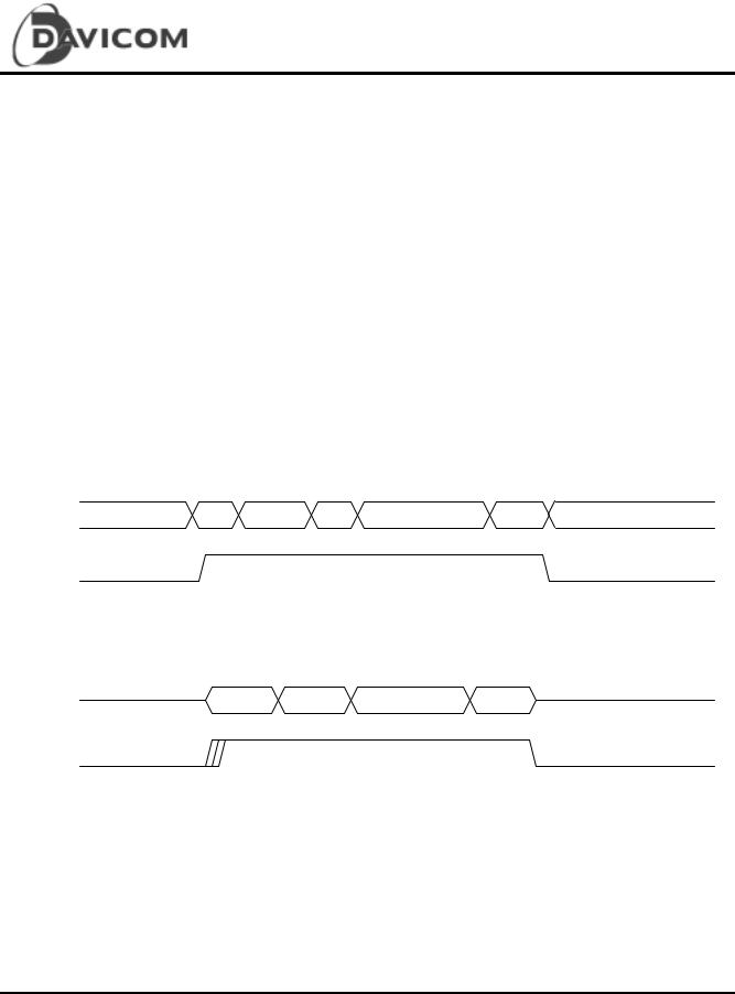
•CRS (carrier sense) is asserted by the PHY when either the transmit or receive medium is non-idle and deasserted by the PHY when the transmit and receive medium are idle. Figure 2 depicts the behavior of CRS during 10Base-T and 100Base-TX transmission.
T X D |
IDLE |
SSD |
Preamble |
SFD |
Data |
ESD |
IDLE |
|
J/K |
T/R |
|||||||
|
|
|
|
|
|
|||
C R S |
|
|
|
100Base-TX |
|
|
|
|
|
|
|
|
|
|
|
T X D |
Preamble |
SFD |
Data |
EFD |
10Base-T
C R S
Figure 2
Final |
13 |
Version: DM9101-DS-F03
July 22, 1999
 Loading...