

Davicom DM9131 Datasheet
DM9131
10/100 Mbps Fast Ethernet Physical Layer Si ngle Chi p Transceiver
Final 1
Version: DM9131-DS-F01
April 7, 2000
General Description
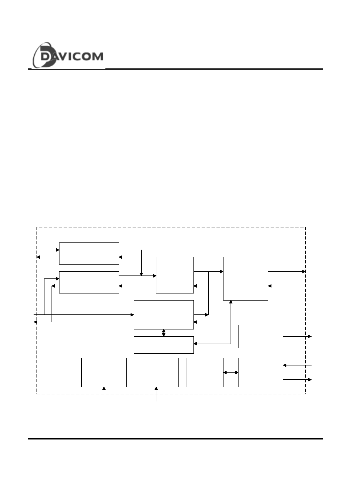
The DM9131 is a physical-layer, single-chip, lowpower transceiver for 100BASE-TX and 10BASE-T
operations. On the media side, it provides a direc t
interface either to Unshielded Twisted Pair Cable 5
(UTP5) for 100BASE-TX Fast Ethernet, or
UTP5/UTP3 Cable for 10BASE-T Ethernet, and it also
provides PECL interface to connect the external fiber
optical transceiver. Through the Media Independent
Interface (MII), the DM9131 connects to the Medium
Access Control (MAC) layer, ensuring a high interoperability among products from different vendors.
The DM9131 uses a low-power and high-performance
CMOS process. It contains the entire physical layer
functi ons of 100BASE-TX as defined by IEEE802.3u,
including the Physical Coding Sublayer (PCS),
Physical M edium A ttachm ent (PMA), Twisted Pair
Physical Medium Dependent Sublayer (T P-PMD),
10BASE-TX Encoder/Decoder (ENC/DEC), and
Twisted Pair Media Access Unit (TPMAU). The
DM9131 provides a strong support for the autonegotiation function utilizing automatic media speed
and protocol selection. Furthermore, due to the builtin wave-shaping filter, the DM9131 needs no external
filter to transport signals to the media in 100M or 10M
Ethernet operat ion.
Block Diagram
MII
Management
Control
Biasing/
Power
Block
Clock
Circuit
Block
100Base-TX
Transceiver
100Base-FX
PECL
Interface
LED Driver
MII
Interface
MII
Register
100Base-
TX
PCS
10Base-T
TX/RX Module
Auto-Negotiation

DM9131
10/100 Mbps Fast Ethernet Physical Layer Si ngle Chi p Transceiver
2 Final
Version: DM9131-DS-F01
April 7, 2000
Table of Contents
General Descri pt ion................................................1
Block Diagram........................................................1
Features.................................................................3
Pin Configuration: DM9101E LQFP ........................4
Pin Description.......................................................5
T
Normal MII Interface, 21 pins...............................5
T
Media Interface, 5 pi ns........................................6
T
LED Inte r face, 5 pins...........................................6
T
Mode, 11 pins......................................................7
T
Bias and Clock, 6 pins .........................................7
T
Power and Others, 52 pins...................................8
Functional Description
T
Transmit Section.................................................9
T
100Base-TX Operati on ........................................9
T
MII Serial Management Int er face.........................9
T
Management I nterfac e – Read Frame Structure ..9
T
Management I nterfac e – Write Frame Structure .9
MII Register Description........................................10
- Key To Default ...................................................10
Basic Mode Control Register (BMCR) - 00............ 11
Basic Mode Status Register (BMSR) - 01 .............12
PHY ID Identifier Register #1 (PHYIDR1) - 02 ......13
PHY ID Identifier Register #2 (PHYIDR2) - 03 ......13
Auto-negotiation Advertisement Register (ANAR)
- 04.......................................................................14
Auto-negotiation Link Partner Ability Register
(ANLPAR) - 05......................................................15
Auto-negotiation Expansion Register (ANER)
- 06.......................................................................16
DAVICOM Specified Configuration Register (DSCR)
- 16.......................................................................16
DAVICOM Specified Configuration and Status
Register (DSCSR) - 17 .........................................18
10Base-T Configuration / S tatus (10BTCSR) - 18 .19
DAVICOM Specified Interrupt Register - 21..........20
DAVICOM Specified Receive Error Counter Register
(RECR) - 22.........................................................20
DAVICOM Specified Disconnect Counter Register
(DISCR) - 23........................................................20
Abso lu te Maximum Ratings..................................21
T
Operating Conditions.........................................21
DC Electrical Characte r istics................................22
AC Electrical Char ac teristi cs & Timing Waveform s
............................................................................22
T
TP Interface......................................................22
T
Oscillator/Crystal Timing...................................22
T
MDC/MDIO Timing............................................23
T
MDIO Timing when OUTPUT by STA ...............23
T
MDIO Timing when OUTPUT by DM9131.........23
T
MII 100Base-TX Tr ansmit T iming Parameters... 24
T
MII 100Base-TX Tr ansmit T imi ng Diagram........24
T
MII 100Base-TX Receive Timing Parameters....24
T
MII 100Base-TX Receive Timing Diagram.........25
T
MII 10Base-T Nibble Transmit T iming Parameters
.........................................................................25
T
MII 10Base-T Nibble Transmit T iming Diagram.25
T
MII 10Base-T Receive Nibble Timing Parameters
.........................................................................26
T
MII-10Base-T Receive Nibble Timing Diagram..26
T
Auto-negotiation and Fast Link Pulse Timing
Parameters.......................................................26
T
Auto-negotiation and Fast Link Pulse Timing
Diagram............................................................27
Package Information ............................................28
Ordering Information............................................29
Disclaimer............................................................29
Company Overview..............................................29
Product ................................................................29
Warning...............................................................29
Contact Windows .................................................29

DM9131
10/100 Mbps Fast Ethernet Physical Layer Si ngle Chi p Transceiver
Final 3
Version: DM9131-DS-F01
April 7, 2000

DM9131
10/100 Mbps Fast Ethernet Physical Layer Si ngle Chi p Transceiver
4 Final
Version: DM9131-DS-F01
April 7, 2000
Features
T
Fully compliant with IEEE 802.3u 10Base-T/100Base-
TX
T
Compliant with ANSI X3T12 TP - PMD 1995
standard
T
Support Auto-Negotiation function, compliant to IEEE
802.3u
T
Single-chip fully integrated Physical layer interface -
directly to magnetic
T
Integrated 10Base-T and 100Base-TX transceiver
T
On-chip filtering, no need for external filter s
T
Selectable repeater or node mode
T
Far end fault signaling option in FX mode
T
Selectable twisted-pair or fiber mode output
T
Selectable f ul l -dupl ex or half -dupl ex operati on
T
MII management interface with maskable interrupts
output capability
T
Provides Loopback mode for easy system
diagnostics
T
Status LED ou tput p rovides Link & Activity,
Speed10/100 and Full-duplex/Collision LED
T
Low-Power, Single-Supply 3.3V CMOS technology
T
Compatible with 3.3V and 5.0V tolerant I/O
T
100-pin LQFP
DM9131
10/100 Mbps Fast Ethernet Physical Layer Si ngle Chi p Transceiver
Final 5
Version: DM9131-DS-F01
April 7, 2000
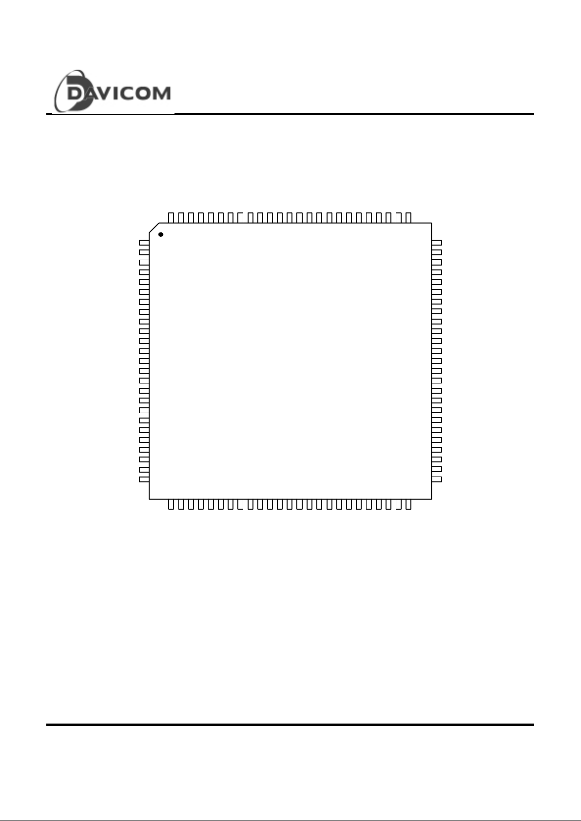
Pin Configuration
11
DM9131
75
74
73
72
71
70
69
68
67
66
65
64
63
62
61
60
59
58
57
55
54
53
52
51
50
49
48
47
46
45
44
43
42
41
40
39
38
37
35
34
33
32
31
30
29
28
27
85
86
87
88
89
90
91
92
93
94
95
96
97
98
99
100
76
77
78
79
80
81
82
83
84
NC
NC
RESET#
NC
DVCC
RXER/RXD[4]/RPTR
RXDV
COL
NC
RXEN
CRS/BP4B5B
RXCLK
MDINTR#
NC
RXD[0]
RXD[1]
RXD[2]
RXD[3]
NC
DVCC
MDIO
MDC
NC
NC
1
2
3
4
5
6
7
8
9
10
12
13
14
15
16
17
18
19
20
21
22
23
24
25
NC
NC
DGND
NC
TXCLK
RMII
NC
DVCC
TXEN
TXD[0]
NC
TXD[1]
TXD[2]
TXER/TXD[4]
NC
DGND
TXD[3]
LINKLED
LINK&ACTLED#
FDX/COLLED#
TRFLED#
DVCC
SPEEDLED#
PWRDWN
NC
NC
TESTMODE
PHYADR4
PHYADR3
PHYADR2
PHYADR1
PHYADR0
NC
DGND
NC
XT2
OSCSEL
OSCIN/REF_CLK
NC
DVCC
NC
XT1
NC
DGND
AGND
NC
SD
NC
AVCC
NC
NC
BGRESG
BGRES
NC
AVCC
RX+/FXRD+
RX-/FXRD-
AVCC
AGND
AGND
AGND
AGND
TX+/FXTD+
TX-/FXTD-
NC
AVCC
PLLVCC
NC
PLLGND
DGND
NC
OPMODE0
OPMODE1
OPMODE2
NC
26
36
56
NC

DM9131
10/100 Mbps Fast Ethernet Physical Layer Si ngle Chi p Transceiver
6 Final
Version: DM9131-DS-F01
April 7, 2000
Pin Description
I : Input, O : Output, LI : Latch input when power-up/reset, Z : Tri-State output
Normal MII interface, 21 pins
Pin No. Pin Name I/O Descriptio n
38 TXER/TXD[4] I Transmit Error/The fifth TXD data bit
In 100Mbps mode, when the signal actives high and TXEN actives, the
HALT symbol is sub stituted for the actual data nibble. In 10Mbps, the
input is ignored.
In bypass mode (bypass BP4B5B), TXER becomes the TXD[4] pin, the
fifth TXD data bit of the 5B symbol.
42,41,40,39 TXD[0:3] I Transmit Data
4 bits nibble data input (synchronous to the TXCLK) when in 10/100Mbps
nibble mode.
In 10Mbps serial mode, the TXD[0] pin is used as the serial data input pin,
and TXD[1:3] are ignored.
43 TXEN I Transmit Enable
Active high to indicate the presence of valid nibble data on the TXD[0:3]
for both 100Mbps and 10Mbps nibble mode.
In 10Mbps serial mode, active high indicates the presence of valid
10Mbps data on TXD[0].
47 TXCLK O,Z Transm it Clock
The transmitting clock provides the timing reference for the transfer of the
TXEN, TXD, and TXER. T XCLK i s provi ded by th e PH Y.
25MHz in 100Mbps nibble mode, 2.5MHz in 10Mbps nibble mode, 10MHz
in 10Mbps serial mode.
53 MDC I Management Data Clock
Synchronous clock for the MDIO management data. This clock i s
provided by management entity, and it is up t o 2.5 MH Z
54 MDIO I/O Management Dat a I/O
Bi-directional management data that may be provided by the station
management entit y or the PHY.
61,60,59,58 RXD[0:3] O,Z Receive Data Output
4 bits nibble data output (synchronous to RXCLK) when in 10/100Mbps
nibble mode.
In 10Mbps serial mode, the RXD[0] pin is used as the serial data output
pin, and the RXD[1:3] are ignored.
63 MDINTR# O Status Interrupt Output :
Asserted low whenever there is status change.(link, speed, duplex )
64 RXCLK O,Z Receive Clock,
The received clock provides the timing reference for the transfer of the
RXDV, RXD, and RXER. RXCLK is provided by PHY. The PH Y may
recover the RXCLK reference from the received data or it may derive the
RXCLK r efere nce from a nominal clock.
25MHz in 100Mbps nibble mode, 2.5MHz in 10Mbps nibble mode, 10MHz
in 10Mbps serial mode.
65 CRS/( BP4B5B ) O,Z
/LI
Carrier Sense Detect/Bypass 4B/5B encoder/decoder
Asserted high to indicate the presence of carrier dues to receive or

DM9131
10/100 Mbps Fast Ethernet Physical Layer Si ngle Chi p Transceiver
Final 7
Version: DM9131-DS-F01
April 7, 2000
transmit activities in 10BASE-T or 100BASE-TX half-duplex mode. In
repeater mode or full-duplex mode, this signal is asserted high to indicate
the presence of carrier due only to the receive activity.
This pin is also used as bypass 4B/5B encoder/decoder.(power up reset
latch input)
0 = normal operation
1 = bypass 4B5B
66 COL O,Z Collisio n De t ectio n
Asserted high to indicate that detection of the collision conditions in
10Mbps and 100Mbps half-duplex mode. In full-duplex mode, this signal
is always logical 0.
67 RXDV O,Z Receive Data Valid
Asserted high to indicate that the valid data is present on the RXD[0:3].
68 RXER/RXD[4]
/(RPTR/NODE)
O,Z
/LI
Receive Data Error/The fifth RXD data bit of the 5B symbol
Asserted high to indicate that an invalid symbol has been detected.
In decoder bypass mode (bypass BP4B5B), RXER becomes RXD[4], the
fifth RXD data bit of the 5B symbol.
These pins are also used to select Repeater or Node mode. (power up
reset latch i nput).
0 = node mode (default)
1 = repeater mode
69 RXEN I Receive Enable :
Active high enable for receive signals RXD[0:3], RXCLK, R XDV and
RXCLK. A low on this input tri-states t hese output pins. For normal
operation in a node application, this pin should be pulled high. In repeater
application, this pin may be connected to a repeater controller.
73 RESET# I Reset
Active low input that initializes the DM9131.
Media interface, 5 pins
Pin No. Pin Name I/O Descript ion
7,8 RX+/FXRD+
RX-/FXRD-
I Differential receive pair/PECL receive pair
Differential data is received from the media.
Differential Pseudo ECL signal is received from the media in fiber mode.
13,14
TX+/FXTD+
TX-/FXTD-
O Differential t r ansmit pair/PECL transmit pair
Differential data is transmitted to the media in TP mode.
Differential Pseudo ECL signal transmits to the media in fiber mode.
97 SD I Fiber-optic signal detect
PECL signal which indicates whether or not the fiber-optic receive pair is
receiving valid signal levels.
LED interface, 5 pins
Pin No. Pin Name
I/O
Description
31 TRFLED# O Traffic LED
Active low. It flashes when the DM9131 is transmitting or receiving data.
32 FDXLED
/COLLED#
O Full-Duplex LED/Collision LED :
Active low. Indicates f ull-duplex mode for 100Mbps and 10Mbps
operation. It is changed to collision LED function when bit 4 of register 16
is set to 1.

DM9131
10/100 Mbps Fast Ethernet Physical Layer Si ngle Chi p Transceiver
8 Final
Version: DM9131-DS-F01
April 7, 2000
33 SPEEDLED# O Speed LED:
Driven low when operating in 100Mbps and high when operating in
10Mbps.
When bit 6 of Register 16 is set, it controls the SPEEDLED as 100BaseTX SD signal output . For debug onl y.
34 LINK&ACT LED# O Link LED & Activity LED :
Active low to indicate good link for 10Mbps and 100Mbps operation. It i s
also a activity LED function when transmit or receive data.
35 LINKLED O Link LED
Active high to indicate good link for 10Mbps and 100Mbps operation
Mode, 11 pins
Pin No. Pin Name I/O Descript ion
22,23,24 OPMODE0~2 LI OPMODE0~OPMODE2 :
These pins are used to control the forced or advertised operating mode of
the DM9131 according to the following table. The value is latched into the
DM9131 registers at power-up/reset.
OP2 OP1 OP0 Function
0 0 0 auto negotiation enable with all capabilities
0 0 1 manual select 100TX FDX
0 1 0 manual select 100TX HDX
0 1 1 manual select 10TX FDX
1 0 0 manual select 10TX HDX
1 0 1 manual select 100FX FDX
1 1 0 manual select 100FX HDX
1 1 1 dual speed 100/10 HDX
27 RMII I Reduced MII enable:
This pin is used to select Normal MII or Reduced MII.
“0”= Normal MII, (default)
“1”= Reduced MII.
This pin always pull-low except that DM9131 is used as reduce d MII.
28 PWRDWN I Power down control
Assert high to force DM9131 into power down mode. When in power down
mode, most of the DM9131 circui t block’s power is truned off , only the MII
management interface (MDC, M DIO) logic is available (the PHY should
respond to management transactions and should not generate spurious
signals on the MII)). To leave power down mode, DM9131 need the
hardware or software reset with the PWRDWN pin to low.
77 T E S TMODE I Test mode control pi n.
0 = normal operation
1 = enable test mode
82~78 PHYADR[0:4] I
PHY address
PHY address sensing input pins.

DM9131
10/100 Mbps Fast Ethernet Physical Layer Si ngle Chi p Transceiver
Final 9
Version: DM9131-DS-F01
April 7, 2000
Bias and clock, 6 pins
Pin No. Pin Name I/O Descript ion
2 BGRESG P Bandgap Ground
3 BGRES P Bandgap Voltage Reference Resistor 6.2K ohm
86 OSCSEL I Oscillator or Crystal selection. “0” = Crystal, “1” = Oscillator
87 OSCIN
/ REF_CLK
I Oscillator input (25MHz) or Reduced M II Ref erence Cl ock Input ( 50MHz
for Reduced MII only).
91 XT2 O Crystal Output
92 XT1 I Crystal I nput
Power and o thers, 52 pins
Pin No. Pin Name I/O Descript ion
5,6,16,99 AVCC P Analog Power
9,10,11,12,95 AGND P Analog Ground
30,45,56,71,
89
DVCC P Digital Power
20,36,49,84
,94
DGND P Digit al Ground
17 PLLVCC P Analog Power
19 PLLGND P Analog Ground
1,4,15,18,21,
25,26,29,37,
44,46,48,50,
51,52,55,57,
62,70,72,74,
75,76,83,85,
88,90,93,96,
98,100
NC Not connected.
 Loading...