

Davicom DM9102AT, DM9102AF Datasheet
General Descri ption
DM9102A
Single Chi p Fast E thern et NIC c ont roller
The DM9102A is a fully integrated and cost-effective single
chip Fast Ethernet NIC controller. It is designed with the low
power and high performance process. It is a 3.3V device
with 5V tolerance then it s upports 3.3 V and 5V signaling.
The DM9102A provides direct interface to the PCI or the
CardBus. It supports bus master capability and fully
complies with PCI 2.2. In media side, The DM9102A
interfaces to the UTP3,4,5 in 10Base-T and UTP5 in
100Base-TX. It is fully compliance with the IEEE 802.3u
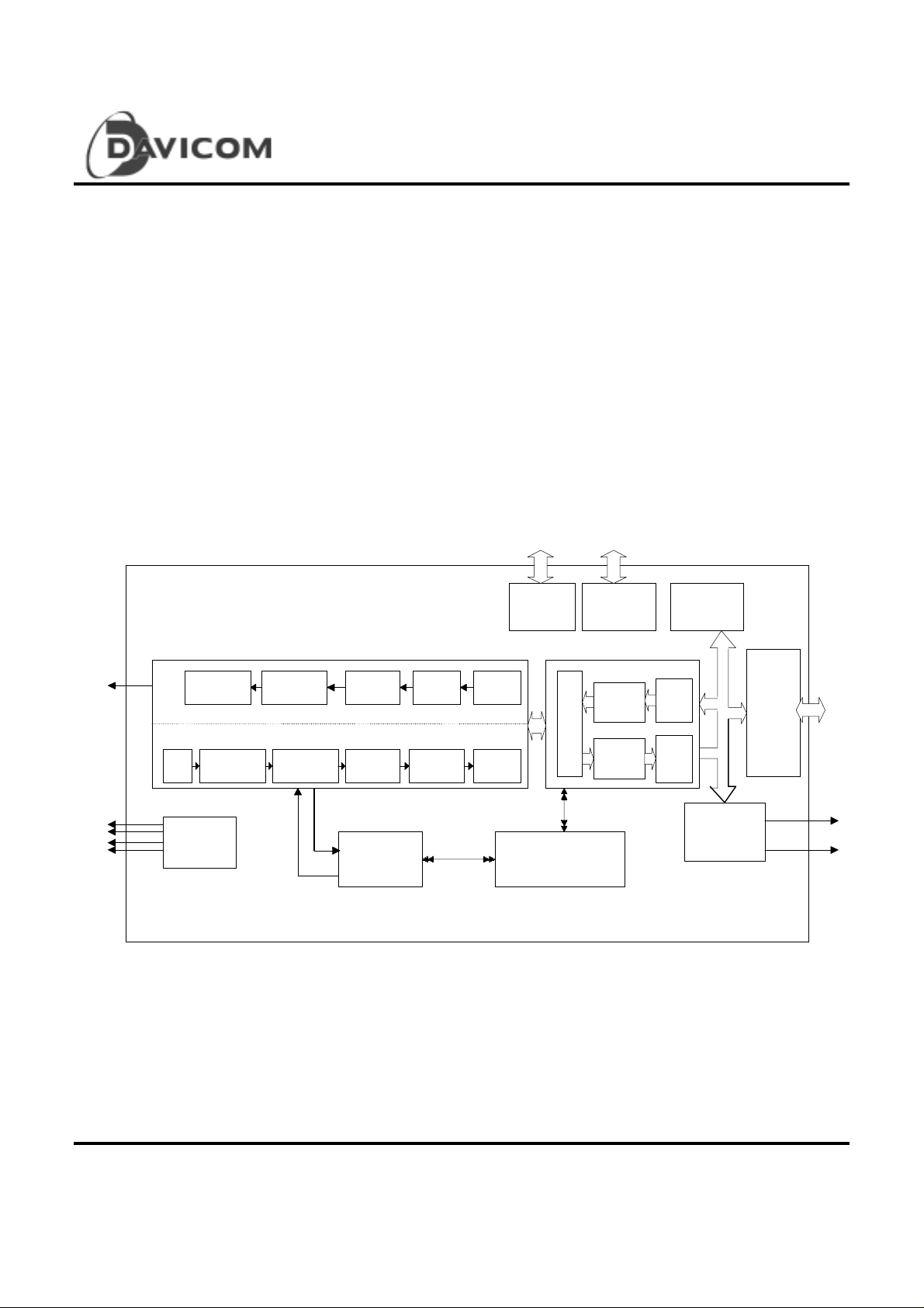
Block Diagr am
PHYceiver
TX+/-
RX+/-
MLT3 to NRZI NRZI to NRZ
AEQ
NRZ to NRZINRZI to MLT3
Parallel to
Serial
Parallel to
Serial
Scrambler
Scrambler
De-
Spec. Its auto-negotiation function will automatically
configure the DM9102A to take the maximum advantage of
its abilities. The DM9102A is also support IEEE 802.3x fullduplex flow control.
The DM9102A supports two types of power-management
mechanisms. The main mechanism is based upon the
OnNow architecture, which is required for PC99. The
alternative mechanism is based upon the remote Wake-OnLAN mechanism.
4B/5B
Encoding
4B/5B
Decoding
EEPROM
Interface
Boot ROM /
MII Interface
MAC
Machine
MII
MachineRXFIFO
TX
RX
TX
FIFO
DMA
PCI
Interface
Power
LED Driver
Autonegotiation
Final 1
Version: DM9102A-DS-F03
August 28, 2000
MII Management Control
& MII Register
Management
Block
PME#
WOL

Table of Conten ts
DM9102A
Single Chi p Fast E thern et NIC c ont roller
General Description .............................................................1
Block D iag ra m...................................................................... 1
Feature s...............................................................................4
Pin Configuration: DM9102A 128pin QFP..........................5
Pin Configuration: DM9102A 128pin TQFP .......................6
Pin De sc ript ion.....................................................................7
- PCI Bus and CardBus Interface Signals.........................7
- Boot ROM and EEPROM Interface................................8
T
Multip lex M ode ................................................................8
T
Direct M ode....................................................................10
- LED P ins.........................................................................11
- Netw ork Inter face...........................................................1 2
- Miscellaneous Pins.........................................................12
- Pow er Pin s.....................................................................13
- Note: L E D M ode............................................................13
Regis ter De fin ition..............................................................14
✧ PC I C on figu rat ion R egis ter s..........................................14
Key to De faul t.....................................................................14
T
Identification ID...............................................................15
T
Command & Status........................................................15
T
Revisio n ID.....................................................................17
T
Miscellaneous Function .................................................18
T
I/O Bas e Add res s...........................................................18
T
Memory Mapped Base Address....................................19
T
Subsystem Identification................................................19
T
CardBu s CIS P oi nter......................................................20
T
Expansion ROM Base Address.....................................21
T
Capabilities Pointer.........................................................21
T
Interrupt & Latency Configuration..................................22
T
Device Spe ci fic Configuration Register.........................22
T
Power Management Register........................................23
T
Power Management Control/Status..............................24
✧ C ontr o l and Sta tu s R eg iste r ( CR)..................................25
Key to De faul t.....................................................................25
1. System Cont rol Re gist er (CR0).....................................2 6
2. Trans mi t Des cr ipto r Po ll D ema n d (CR 1)......................2 7
3. Receive Descriptor Poll Demand (CR2).......................27
4. Rece i ve D es cripto r Bas e Ad dre ss (C R3).....................27
5. Trans mi t Des cr ipto r Bas e Add res s (CR 4)....................28
6. Network Status Report Register (CR5).........................28
7. Netw or k Ope rat ion R egis ter (C R6)...............................30
8. Interru p t Mas k Register (C R7)...................................... 32
9. Statistical Counter Register (CR8)................................ 33
10. PROM & Management Access Register (CR9) ........ 34
11. Prog ra mmi ng R OM Add res s Re gis ter ( CR 10).......... 35
12. General Purpose Timer Register (CR11)................... 35
13. PHY S tatu s R eg is ter (CR 12)...................................... 35
14. Sa mple Fra m e A cc es s Reg iste r (CR1 3).................... 36
15. Sa mple Fra m e D a ta Reg is ter (C R14)........................ 36
16. Watching & Jabber Timer Register (CR15)................ 36
✧ CardBus Status Changed Register..............................39
1. Function Event Reg ister : (offs et 80 h)............................ 39
2. Function Event Mask Register: (offset 84h).................. 39
3. Fun ctio n P res en t S tate Re gis ter : (o ffse t 8 8h )............... 39
4. Fun ctio n Fo rce E ven t Re g iste r: (o ffse t 8 Ch)................4 0
✧ PHY Manage ment Register Set...................................41
Key To D efau lt................................................................... 41
Basic Mode Control Register (BMCR)
- Regis ter 0......................................................................... 42
Basic Mode Status Register (BMSR)
- Regis ter 1......................................................................... 43
PHY ID Identifier Register #1 (PHYIDR1)
- Regis ter 2......................................................................... 44
PHY ID Identifier Register #2 (PHYIDR2)
- Regis ter 3......................................................................... 44
Auto-negotiation Advertisement Register (ANAR)
- Regis ter 4......................................................................... 44
Auto-negotiation Link Partner Ability Register (ANLPAR) -
Regis ter 5........................................................................... 45
Auto-negotiation Expansion Register (ANER)
- Regis ter 6......................................................................... 46
DAVICOM Specified Configuration Register (DSCR)
- Regis ter 10....................................................................... 46
DAVIC OM S pec i fied Co n figura tio n a n d Status Regi ste r
(DSCSR ) - R eg iste r 11...................................................... 47
10Base-T Configuration/Status (10BTSCRCSR)
- Regis ter 12....................................................................... 48
Functio na l D es cr ip tio n....................................................... 49
✧ System Buffer Management ......................................... 49
1. Over view........................................................................ 49
2. Data Structure and Descriptor List................................49
3. Buffer Management: Chain Structure Method.............. 49
5. Des crip tor L ist: Bu ffer De s crip tor Fo r mat...................... 49
(a). Re ce i ve Des cr ipto r Fo rma t......................................... 49
2 Final
Version: DM9102A-DS-F03
August 28, 2000

DM9102A
Single Chi p Fast E thern et NIC c ont roller
6. Example of DM9102A SROM Format.......................... 63
(b). Tran s mit D es cripto r For mat .........................................51
✧ Initialization Procedure...................................................54
Data Bu ffer Proce ss ing A lgor ith m.....................................54
1. Rece i ve D ata Bu ffer Pro ces s ing...................................54
2. Trans mi t Da ta Bu ffer Pr oce ss ing..................................55
✧ N etw or k Fun c tion...........................................................56
1. Over view.........................................................................56
2. Receive Process and State Machine............................56
a. Reception Initiation ....................................................... 56
b. Address Recognition....................................................5 6
c. Frame Decapsulation...................................................56
3. Transmit Process and State Machine...........................56
a. Transmit Initiation.......................................................... 56
b. Fr a me En cap s ula tion...................................................56
c. Collision ......................................................................... 56
4. Phys ica l Lay er O ver view...............................................56
✧ Serial Management Interface........................................57
✧ Power Management ......................................................5 8
1. Over view.........................................................................58
2. PCI Function Power Management Status ....................58
3. The Power Management Operation .............................58
a. Detect Netw ork Link State Change.............................58
b. A cti ve M ag ic Pack e t Func tion ......................................58
c. Acti ve the Sam ple F rame Fu nctio n.............................58
✧ Sa mp le Fra me P rog ra mmi ng Gu ide.............................60
Serial RO M O ver view........................................................61
1. Subs ys te m ID B loc k.......................................................61
2. SROM Ve rs ion...............................................................6 2
3. Controller Count.............................................................62
4. Contr o ller_ X In for mat ion................................................62
5. Controller Information Body Pointed By Controller_X Info
Block Offset It em in Co ntro ller Inform ation Header.......62
Externa l MII/ SRL In ter face................................................66
The Sha ring Pin Ta ble....................................................... 66
Abso lute Ma ximu m Ra ting s..............................................6 8
Operat ing Co nd itions......................................................... 68
DC Electrical Characteristics ............................................. 69
AC Elec tr ica l Ch ara cte r istic s & T imin g Wa vefo rms ..........70
T
PCI Clo ck Spe c . Ti ming.................................................7 0
T
Other P C I Sig na ls Ti ming Dia gra m............................... 70
T
Multip lex M ode Boo t ROM Tim ing................................ 71
T
Direct Mode Boot ROM Timing..................................... 72
T
EEPROM Ti ming........................................................... 72
T
TP Inter face....................................................................73
T
Oscil lator/C rysta l Ti ming................................................ 73
T
Auto-negotiation and Fast Link Pulse Timing Parameters
........................................................................................ 73
Package Information (128 pin, QFP) ................................ 75
Package Information (128 pin, TQFP).............................. 76
Order ing In forma tion.......................................................... 77
Discla imer..........................................................................7 7
Company Overview........................................................... 77
Products.............................................................................77
Contact Windows...............................................................77
Warnin g.............................................................................. 77
Final 3
Version: DM9102A-DS-F03
August 28, 2000

Features
T
Integrated F ast Et hernet MAC, Physical Layer and
transceiver i n one chip.
T
128pin QFP/128pin TQFP with CMOS process.
T
+3.3V Power supply with + 5V tolerant I/O.
T
Supports PCI and CardBus interfaces.
T
Comply with PCI specification 2.2.
T
PCI clock up to 40MHz.
T
PCI bus m aster architecture.
T
PCI bus burst mode data transfer.
T
Tw o large independent FIFO; receive FIFO & transmit
FIFO.
T
Up to 256K bytes Boot EPROM or Flash interface.
T
EEPROM 93C46 i nterface supports node ID accesses
configuration inform ation and user define message.
T
Node address auto-load and reload.
T
Comply with IEEE 802.3u 100Base-TX and 802.3
10Base-T.
T
Comply with I EEE 802.3u auto-negot iation protocol f or
DM9102A
Single Chi p Fast E thern et NIC c ont roller
automatic link type selecti on.
T
Full Dup lex/Half Duplex capabil ity.
T
Support IE EE 802.3x Full Duplex Flow Contro l
T
VLAN support.
T
Comply with ACPI and PCI Bus Power Management.
T
Supports the MII (Media Independent Interface).
T
Supports Wake-On-LAN function and remote wake-up
(Magic packet, Link Change and Microsoft
frame) .
T
Supports 4 Wake-On-LAN (WOL) signals (active high
pulse, active low pulse, active high , active low ).
T
High performance 100Mbps clock generator and data
recovery circuit.
T
Dig ita l clo c k r ec o ver y c irc u it us in g advanc e d digital
algorithm to reduce jitt er.
T
Adaptive equalization circuit and Baseline wandering
restoration c ircuit for 100Mbps receiver.
T
Provides Loopbac k m ode for easy system diagnostics.
®
wake-up
4 Final
Version: DM9102A-DS-F03
August 28, 2000

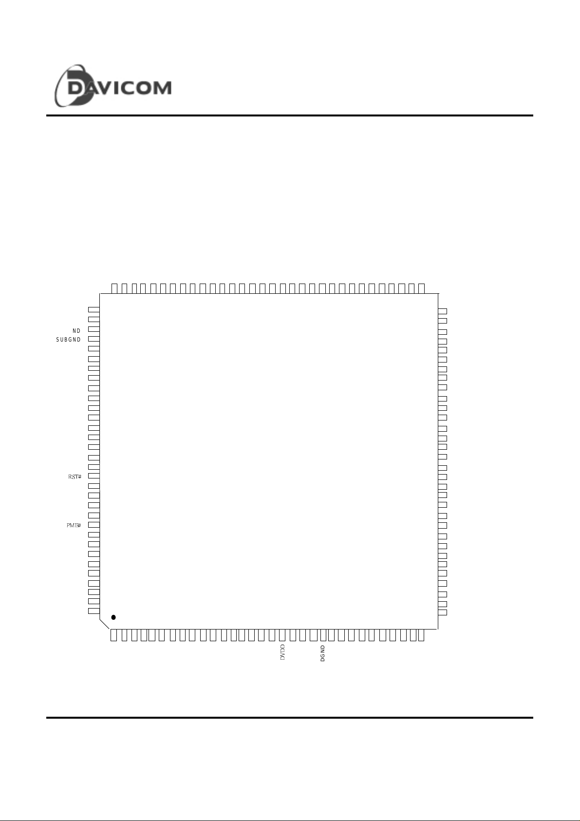
Pin Configuration : 128 pin QFP
DM9102A
Single Chi p Fast E thern et NIC c ont roller
AVDD
AVDD
RXI+
RXIAGND
AGND
TXO+
TXO-
AVDD
AVDD
INT#
RST#
PCICLK
ISOLATE#
GNT#
REQ#
PME#
DVDD
AD31
AD30
AD29
AD28
DGND
AD27
AD26
AD25
BGRES
BGRESG
X1/OSCX2DGND
SUBGND
99
98
100
102
101
103
104
105
106
107
108
109
110
111
112
113
114
115
116
117
118
119
120
121
122
123
124
125
126
127
128
123456789
WOL/CSTSCHG
MA16
MA15
MA17
MA14
(MA11/FDX#)
(MA12 / SPEED100#)
(MA13/SPEED10#)
DVDD
WOL/CSTSCHG
NC
94
95
97
96
SPEED10#
FDX#
SPEED100#
NC
NC
NC
88
89
90
91
92
93
(MA8)
(MA9)
(MA10/LINK&ACT#)
LINK&ACT#
87
(MA7)
NC
NC
NC
DGND
86
DVDD
84
82
83
85
(MA6/SELROM)
SELROM
81
(MA4/EECK)
(MA5)
EECK
EECS
807978
(MA3/EEDO)
EEDO
(MA2)
EEDI
77
DGND
TEST1
767574
(MA1/PCIMODE#)
BPA0/WMODE2
BPA1/PCIMODE#
73
BPCS#
TEST2
727170
(MD7/LEDMODE)
BPAD7/LEDMODE
DVDD
6968676665
(ROMCS)
(MA0/WMODE)
DM9102A
11
10121314151617181920212223242526282930
27
33
34
32
31
(MD3)
(MD4)
(MD5)
(MD6)
BPAD4
BPAD5
BPAD6
BPAD3
(MD2)
BPAD2
64
63
62
61
60
59
58
57
56
55
54
53
52
51
50
49
48
47
46
45
44
43
42
41
40
39
38
37
36
35
BPAD1
BPAD0
DVDD
AD0
AD1
DGND
AD2
AD3
AD4
AD5
DVDD
DVDD
AD6
AD7
AD8
CBE0#
AD9
DGND
DGND
AD10
AD11
DVDD
AD12
AD13
AD14
(MD1)
(MD0/EEDI)
PERR#
SERR#
PAR
DVDD
CBE1#
AD15
DGND
DGND
CLOCKRUN#
IDSEL
AD23
DVDD
DVDD
AD24
CBE3#
AD21
AD20
AD19
AD18
AD17
AD22
DGND
DVDD
DGND
AD16
DVDD
DVDD
DGND
CBE2#
FRAME#
DVDD
IRDY#
DGND
TRDY#
DGND
DGND
STOP#
DEVSEL#
Final 5
Version: DM9102A-DS-F03
August 28, 2000
Pin Configuration : 128 pin TQFP
MA14
(MA13/SPEED10#)
(MA12/SPEED100#)
(MA11/FDX#)
SPEED10#
SPEED100#
FDX#
88
89
91
90
(MA10/LINK&ACT#)
LINK&ACT#
DGND
86
87
(MA7/WMODE1)
(MA8)
(MA9)
NC
NC
NC
85
83
84
DVDD
82
DM9102A
121314
10
11
1516171819202122232425
(MA5)
(MA6/SELROM)
SELROM
EECS
80
81
X2
X1/OSC
DGND
SUBGND
BGRESG
BGRES
AVDD
AVDD
RXI+
RXIAGND
AGND
TXO+
TXOAVDD
AVDD
INT#
PCICLK
ISOLATE#
GNT#
REQ#
DVDD
AD31
AD30
AD28
DGND
AD27
AD26
AD25
MA16
MA15
MA17
WOL/CSTSCHG
WOL/CSTSCHG
DVDD
96
95
97
98
99
100
101
102
103
104
105
106
107
108
109
110
111
112
113
114
115
116
117
118
119
120
121
122
123AD29
124
125
126
127
128
123456789
NC
94
93
NCNCNC
92
(MA2)
(MA3/EEDO)
(MA4/EECK)
EEDI
EEDO
EECK
DGND
78
76
77
79
DM9102A
Single Chi p Fast E thern et NIC c ont roller
(MD3)
(MD4)
(MD5)
(MD6)
(ROMCS)
(MA0WMODE2)
(MA1/PCIMODE#)
BPCS#
BPA0
BPA1/PCIMODE#
TEST1
747372
75
(MD7/LEDMODE)
TEST2
26
BPAD6
BPAD7/LEDMODE
DVDD
71
706968
28
27
29
BPAD5
BPAD4
66
67
31
30
BPAD3
65
64
63
62
61
60
59
58
57
56
55
54
53
52
51
50
49
48
47
46
45
44
43
42
41
40
39
38
37
36
35
34
33
32
BPAD2
BPAD1
BPAD0
DVDD
AD0
AD1
DGND
AD2
AD3
AD4
AD5
DVDD
DVDD
AD6
AD7
AD8
CBE0#
AD9
DGND
DGND
AD10
AD11
DVDD
AD12
AD13
AD14
AD15
DGND
CLOCKRUN#
DGND
CBE1#
PAR
(MD2)
(MD1)
(MD0/EEDI)
AD24
CBE3#
DVDD
IDSEL
AD23
DVDD
AD22
DGND
AD21
DGND
AD20
AD19
DVDD
AD18
DGND
AD17
AD16
DVDD
CBE2#
IRDY#
DGND
FRAME#
DVDD
TRDY#
DGND
STOP#
DEVSEL#
DGND
PERR#
DVDD
SERR#
6 Final
Version: DM9102A-DS-F03
August 28, 2000

Single Chi p Fast E thern et NIC c ont roller
Pin Descr iption
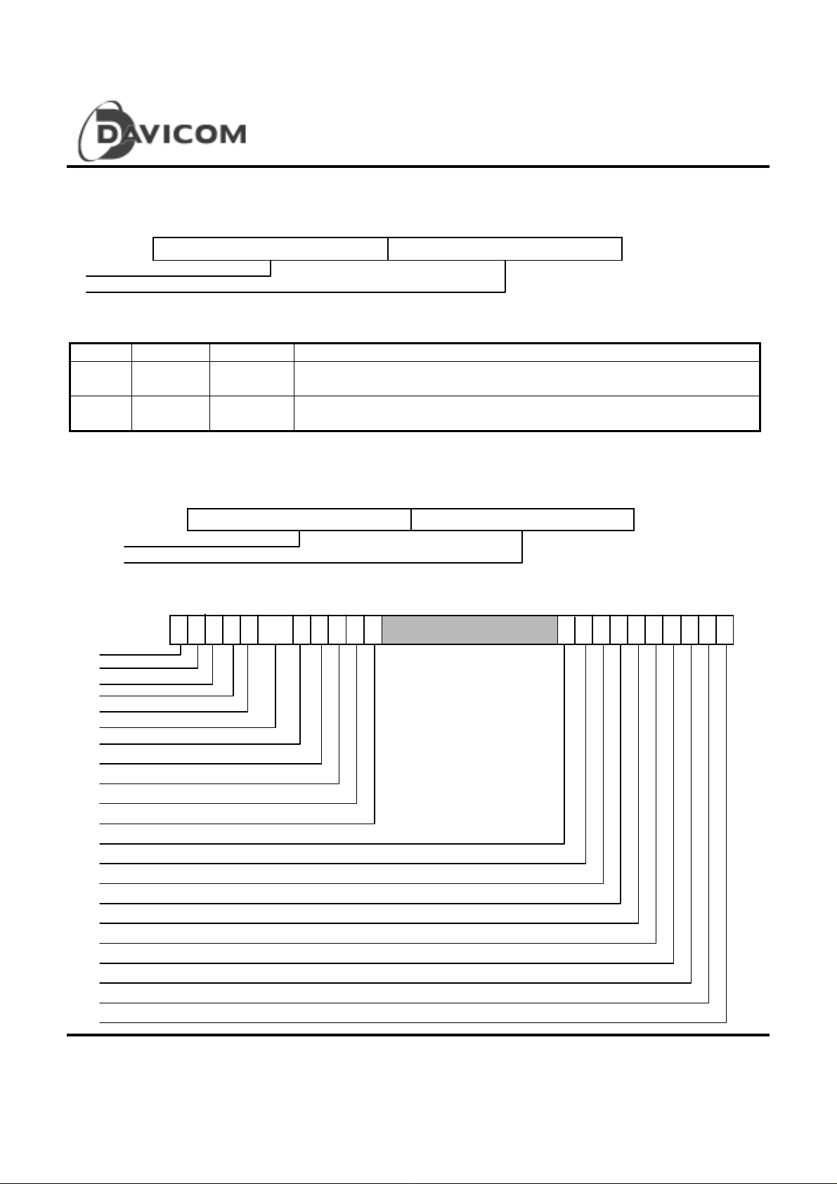
I = Input, O = Out put, I/O = Input / O utput, O/D = Open Drain, P = Power,
LI = reset Latch Input, # = asserted Low
PCI Bus and CardBus Interface Signals
Pin No.
128QFP/128TQFP
113 INT# O/D Interrupt Request
114 RST# I System Reset
115 PCICLK I PCI system clock
117 GNT# I Bus Grant
118 REQ# O Bus Request
119 PME# O/D Power Management Event.
3 IDSEL I Initialization Device Select
21 FRAME# I/O Cycle Fra me
23 IRDY# I/O Initiator Ready
24 TRDY# I/O Target Ready
26 DEVSEL# I/ O Device Se lect
Pin Name I/O Description
This signal will be asserted low when an interrupt condition
as defined in CR5 is set, and the corresponding mask bit in
CR7 is not set.
When this signal is asserted low, DM9102A performs the
internal system reset to its initial state.
PCI bus clock that provides timing for DM9102A related to
PCI bus transactions. The clock frequency range is up to
40MHz.
This signal is asserted low to indicate that DM9102A has
been granted ownership of the bus by the central arbiter.
The DM9102A will assert this signal low to request the
ownership of the bus.
Open drain. Active Low. The DM9102A drive it low to
indicates that a power management event has occurred.
This signal is asserted high duri ng the Configuration Space
read/write access.
This signal is driven low by the DM9102A master mode to
indicate the beginning and duration of a bus transaction.
This signal is driven low when the master is ready to
complete the current data phase of the transaction. A data
phase is completed on any clock both IRDY# and TRDY#
are sampled asserted.
This signal is driven low when the target is ready to complete
the current data phase of the transaction. During a read, it
indicates that valid data is asserted. Du rin g a write, it
indicates the target is prepared to accept d ata.
The DM9102A asserts the signal low when it recognizes its
target address after FRAME# is asserted. As a bus master,
the DM9102A will sample this signal that insures its
DM9102A
Final 7
Version: DM9102A-DS-F03
August 28, 2000

27 STOP# I/O Stop
30 PERR# I/O Parity Error
31 SE RR # I/ O S ys tem Error
33 PAR I/O Parity
2
20
34
48
121,122,123,124,126,127,
128,1,6,7,10,
11,13,14,16,
17,38,39,40,
41,43,44,47,
49,50,51,54,
55,56,57,59,
60
C/BE3#
I/O Bus Command/Byte Enable
C/BE2#
C/BE1#
C/BE0#
AD31~AD0 I/O Address & Data
DM9102A
Single Chi p Fast E thern et NIC c ont roller
destination address of the data tran sfer i s recog nized by a
target.
This signal is asserted low by the target device to request the
master device to stop the current transaction.
The DM9102A as a master or slave will ass ert this signal low
to indicate a parity error on any incoming data.
This signal is asserted low when address parity is detected
with PCICS bit31 (detected parity error) Is enabled. The
system error asserts two clock cycles after the falling address
if an address parity error is detected.
This signal indicates even parity across AD0~AD31 and
C/BE0#~C/BE3# including the PAR pin. This signal is an
output for the master and input for the slave device. It is
s ta b l e and va l id on e c l ock a f t er the address phase.
During the address phase, these signals de fine the bus
command or the type of bus transaction that will take place.
During the data phase these pins indicate which byte lanes
contain valid data. C/BE0# applies to bit7-0 and C/BE3#
applies to bit31-24.
These are multiplexed address and data bus si gnals. As a
bus master, the DM9102A will drive address during the first
bus phase. During subsequent phases, the DM9102A will
either read or write data expecting the target to increment its
address pointer. As a target, the DM9102A will decode each
address on the bus and respond if it is the target being
addressed.
Boot ROM and EEPROM Interface (I ncluding multip lex mode or d irect mode)
Multiple x mo de
Pin No.
Pin Name I/O Description
128QFP/128TQFP
62,63,64,65,
66,67,68,69
BPAD0~BPAD7
(BPAD7/LEDM ODE)
I/O, LI Boot ROM address and data bus (bits 0~7)
Boot ROM address and data multiplexed lines bits 0~7. In
MUX mode, there are two consecutive address cycles, these
lines contain the boot ROM address pins 7~2, out_enable and
write_enable of Boot ROM in the first cycle; and these lines
contain address pins 15~8 in second cycle.
After the first two cycles, these lines contain data bit 7~0 in
consective cycles.
BPAD1 is also a reset latch pin. It is Boot ROM address and
data bu s when normal operation. When at power on reset, it is
used to pull up or down externally through a resister to select
8 Final
Version: DM9102A-DS-F03
August 28, 2000

the WOL as pulse or DC signal.
0 = WOL pulse mode (default)
1 = WOL DC mode
BPAD2 is also a reset latch pin. It is Boot ROM address and
data bu s when normal operation. When at power on reset, it is
used to pull up or down externally through a resister to select
the PME as pulse or DC signal.
0 = PM E pulse mode (default)
1 = PME DC mode
BPAD7 is also a reset latch pin. It is Boot ROM address and
data bu s when normal operation. When at power on reset, it is
used to pull up or down externally through a resister to select
LED mode.
0 = LED mode 0 (default)
1 = LED mode 1
72 BPCS# O Boot ROM Chip Selec t
Boot ROM or external register chip select signal.
73 BPA0/WMODE O, LI Boot ROM address line/WOL mode selection
This multiplexed pin acts as boot ROM address bit 0 output
signal during normal operation. When at power on reset, it
used to select the type of WOL signal.
0 = WOL high active (default)
1 = WOL low active
74 BPA1/PCIMODE# I/O, LI Boot ROM address line / PCI mode selection
This multiplexed pin acts as the boot ROM address bit 1 output
signal during normal operation. When RST# is active (low), it
acts as the input system type. If the DM9102A is used in a
CardBus system, this pin should be connected to a pull-up
resistor; otherwise, the DM9102A consider the host as a PCI
system.
0 = PCI mode (default)
1 = CardBus mode
77
78 EEDO O EEPROM Data Out
79 EECK O EEPROM Serial Clock
80 EECS O EEPROM Chip Select
81 SELROM I Multiplex or Director mode s election
83,84,85,91,92,93,94 NC NC In Multiplex mode, these pins are not connected.
EEDI I EEPROM Data In
The DM9102A will read the contents of EEPROM serially
through this pin.
The DM9102A will use this pin to s erially write opcodes,
addresses and data into the EEPROM.
This p in p r ovid e s th e cl oc k for the EEPR OM d ata tra n sfe r.
This pin will enable the EEPROM during loading of the
Configuration Data.
0 = Multiplex mode (default)
1 = Direct mode
Single Chi p Fast E thern et NIC c ont roller
DM9102A
Final 9
Version: DM9102A-DS-F03
August 28, 2000

Direct mode
Pin No.
128QFP/128TQFP
62 MD0/EEDI I
63,64,65,66,67,68,69 MD1~MD7 I
Pin Name I/O
DM9102A
Single Chi p Fast E thern et NIC c ont roller
Description
Boot ROM data input/EEPROM data in
This is mu ltip le xed pin u se d by EE DI a n d MD0.
When boot ROM is selected, it acts as boot ROM data inp ut .
When ROMCS select the EEPROM, the DM9102A will read
the contents of EEPROM serially through this pin.
Boot ROM data input bus
MD1 is also a reset latch pi n. It is Boot ROM address and
data bu s when normal operation. When at power on reset, it
is used to pull up or down externally through a resister to
select the WOL as pulse or level signal.
0 = WOL pulse mode (default)
1 = WOL level mode
MD2 is also a reset latch pi n. It is Boot ROM address and
data bu s when normal operation. When at power on reset, it
is used to pull up or down externally through a resister to
select the PME as pulse or level s ignal.
0 = PM E pulse mode (default)
1 = PME level mode
MD7 is also a reset latch pi n. It is Boot ROM address and
data bu s when normal operation. When at power on reset, it
is used to pull up or down externally through a resister to
select LED mode.
0 = LED mode 0 (default)
1 = LED mode 1
72 ROMCS O
73 MA0/WMODE O Boot ROM address output line/WOL mode selection
74 MA1/PCIMODE# O, LI Boot ROM address output signal/PCI mode selection
77 MA2 O Boot ROM address output signal
78 MA3/EEDO O Boot ROM address output/EEPROM data out
Boot ROM or EEPROM ch ip se lection.
This multiplexed pin acts as boot ROM address output bus
during normal operation. When RST# is active, it is used to
pull up or down externally through a resister to select WOL
High active or LOW active. (WMODE)
0 = WOL high active (default)
1 = WOL low active
This multiplexed pin acts as a boot ROM address output
signal during normal operation. When RST# is active, it acts
as th e in pu t s ys te m type . If t he DM 9102A is used i n a
CardBus system, this pin should be connected to a pull-up
resistor; otherwise, the DM9102A consider the host as a PCI
system.
0 = PCI mode (default)
1 = CardBus mode
This is multiplexed pin used by MA3 and EEDO.
10 Final
Version: DM9102A-DS-F03
August 28, 2000

79 MA4/EECK O Boot ROM address output/EEPROM serial clock
80 MA5 O Boot ROM address output signal
81 MA6/SELROM O/LI Boot ROM address output/Multiplex or Direct mode selection
83,84,85 MA7~MA9 O Boot ROM address output bus
87 MA10/LINK&ACT# O Boot ROM address output signal/Link & Active LED
88 MA11/FDX# O Boot ROM address output/Full-duplex LED
89 MA12 /
SPEED100#
90 MA13/SPEED10# O Boot ROM address output signal/10Mbps LED
91,92,93,
94
MA14~MA17 O Boot ROM address output bus
O Boot ROM address output/ 100Mbps LED
DM9102A
Single Chi p Fast E thern et NIC c ont roller
When The DM9102A will use this pin to s erially write
opcodes, addresses and data into the EEPROM.
This is multiplexed pin used by MA4 and EECK .
This p in p r ovid e s th e cl oc k for the EEPR OM d ata tra n sfe r.
This multiplexed pin acts as boot ROM address output bus
during normal operation. When RST# is active, it is used as
multiplex and direct mode selection :
0 = Boot ROM interface is in multiplex mode (default)
1 = Boot RO M interface is in direct mode.
In DIR mode , this pin r ep resents the Boot ROM address bit
10 when at the time of boot ROM operation. When Boot
ROM is not accessed, this pin acts as traffic-and- link led in
LED MODE 0 or traffic led in LED MODE 1.
In DIR mode , this pin r ep resents the Boot ROM address bit
11 when at the time of boot ROM operation. When Boot
ROM is not accessed, this pin acts as full-duplex led.
In DIR mode , this pin r ep resents the Boot ROM address bit
12 when at the time of boot ROM operation. When Boot
ROM is not accessed, this pin acts as speed-100 led.
In DIR mode , this pin r ep resents the Boot ROM address bit
13 when at the time of boot ROM operation. When Boot
ROM is not accessed, this pin acts as speed-10 led.
LED Pins (Please refer to p.11 “NOTE: LED Mode” for details.)
Pin No.
128QFP/128TQFP
87 LINK&ACT#
88 FDX#
89 SPEED100#
Final 11
Version: DM9102A-DS-F03
August 28, 2000
Pin Name I/O Description
O LED output pin, active low
/ ACT#
/ FDX#
/ SPEED100#
mode 0 = Link and traffic LED. Active low to indicate normal
link, and it will flash as a traffic LED when tran smit tin g or
receiving.
mode 1 = traffic LED only
O LED output pin, active low
mode 0 = Full duplex LED
mode 1 = Full duplex LED
O LED output pin, active low
mode 0 = 100Mbps LED
mode 1 = 100Mbps LED

90 SPEED10#
Network Inter face
Pin No.
128QFP/128TQFP
105,106 RXI+
109,110 TXO+
Miscellaneous Pins
Pin No.
128QFP/128TQFP
36 CLOCKRUN# I/O,
71 TEST2 I TEST mode control 2
75 TEST1 I TEST mode control 1
95 WOL/CSTSCHG O Wake up signal/Card Status Change
97 X2 O Crystal feedback output pin used for crystal connection only.
98 X1/OSC I
102 BGRES I Bandgap Voltage Reference Resistor.
/ LINK#
Pin Name I/O Description
RX-
TXO-
Pin Name I/O Description
O LED output pin, active low
I 100M/10Mbps differential input pair.
O 100M/10Mbps differential output pair.
O/D
DM9102A
Single Chi p Fast E thern et NIC c ont roller
mode 0 = 10Mbps LED
mode 1 = Link LED
These two pins are differential re ce ive input pair for
100BASE-TX and 10BASE -T. They are capable of receiving
100BASE-TX MLT-3 or 10BASE-T Manchester encoded
data.
These two pins are differential o utput pair for 100BASE-TX
and 10BASE-T. This output pair provides controlled rise and
fall times designed to filter the transmitter output.
Clockrun#
The clockrun# signal is used by the system to pause or slow
down the PCI clock signal. It is used by the DM9102A to
enable or disable suspension of the PCI clock signal or restart
of the PCI clock. When the clockrun# signal is not used, this pin
should connected to an external pull-down resistor.
In normal operation, this pin is pull e d-high.
In normal operation, this pin is pulled lo w.
This is multiplexed pin to provide Wake on LAN signal or Card
Status Change. In a PCI system, it is used as a WOL signal. In
a CardBus system, it is used as the Card Status Change
output signal and is asynchronous to the clock signal. It
indicates that a power management event has occurred in a
CardBus system. The DM9102A can assert t his pin if it detects
link status change, or magic packet, or sample frame. The
default is “normal low, active high pulse”. DM9102A also
support High/Low and Pulse/Level options.
Leave this pin open if oscillator is used.
Crystal or Oscillator input. (25MHZ50ppm)
25MHz Oscillator or series-resonanc e, fundamental
frequency crystal.
12 Final
Version: DM9102A-DS-F03
August 28, 2000

101 BGRESG I For Bandgap circuit
116 ISOLAT E# I Isolate
Power Pins
Pin No.
128QFP/128TQFP
100,107,
108
103,104,
111,112
8,9,15,22,28,29,35,37,45,
46,58,76,86,99,125
4,5,12,18,19,25,32,42,52,
53,61,70,82,96,120
Pin Name I/O Description
AGND P Analog ground
AVDD P Analog power, +3.3V
DGND P Digital ground
DVDD P Dig ita l p o w e r, +3 . 3V
DM9102A
Single Chi p Fast E thern et NIC c ont roller
It connects to a 6200, 1% error tolerance resistor between
th i s p i n and BGRESG pin t o p r o vide a n accurate current
reference for DM9102A..
It is used together with the BGRESG pin.
This isolate signal is used to isolate the DM9102A from the
system, and it is suitable for LAN on motherboard. When
isolate signal is active low, it disables the DM9102A function
and the DM9102A will not drive any outputs and sample inputs.
In this case, the power consumption is minimum.
NOTE :
LED Mode
Pin No.
128QFP/128TQFP
87 LINK&ACT#
88 FDX#
89 SPEED100#
90 SPEED10#
Final 13
Version: DM9102A-DS-F03
August 28, 2000
MODE 0 MODE 1
ACT#
Link and traffic LED
Full-duplex LED
100Mbps LED
10Mbps LED
Traffic LE D
FDX#
Full-duplex LED
SPEED100#
100Mbps LED
LINK#
Link LED

Single Chi p Fast E thern et NIC c ont roller
Register Definition
PCI Configuration Registers
The d efiniti o ns of P CI Co nfi gur a tion Registers are based on
the PCI specification revision 2.2 and provides the
initialization and configuration information to operate the PCI
interface in the DM9102A. All registers can be accessed
The default value of PCI configuration registers after reset.
Description Identifier Address Offset Value of Reset
Identification PCIID 00H 91021282H
Command & Status PCICS 04H 02100007H
Revision PCIRV 08H 02000031H
Miscellaneous PCILT 0CH BIOS determine
I/O Base Address PCIIO 10H System allocate
Memory Base Address PCIMEM 14H System allocate
Reserved -------- 18H - 28H 00000000H
CardBus ICS pointer CIS 24H 00000000H
Subsystem Identification PCISID 2CH load from SROM
Expansion ROM Base Address PCIROM 30H 00000000H
Capability Pointer CAP_PTR 34H 00000050H
Reserved -------- 38H 00000000H
Interrup t & L ate nc y PCIINT 3CH Sys te m al locate b it7 ~0
Device Specific Configuration Register PCIUSR 40H 00000000H
Power Management Register PCIPMR 50H C0310001H
Power Management Control & Status PMCSR 54H 00000100H
with byte, word, or double word mode. As defined in PCI
specification 2.1, read accesses to reserve or
unimplemented registers will return a value of “0.” These
registers are to be described in the following sections.
DM9102A
Key to Defa ult
In the register description that follows, the default column
takes the form <Reset Value>
Where
<Reset Value>:
1 Bit set to logic one
0 Bit set to logic zero
X No default value
14 Final
<Access Type>:
RO = Read only
RW = Read/Write
R/C: means Read / Write & Write "1" for Clear.
Version: DM9102A-DS-F03
August 28, 2000
Single Chi p Fast E thern et NIC c ont roller
DM9102A
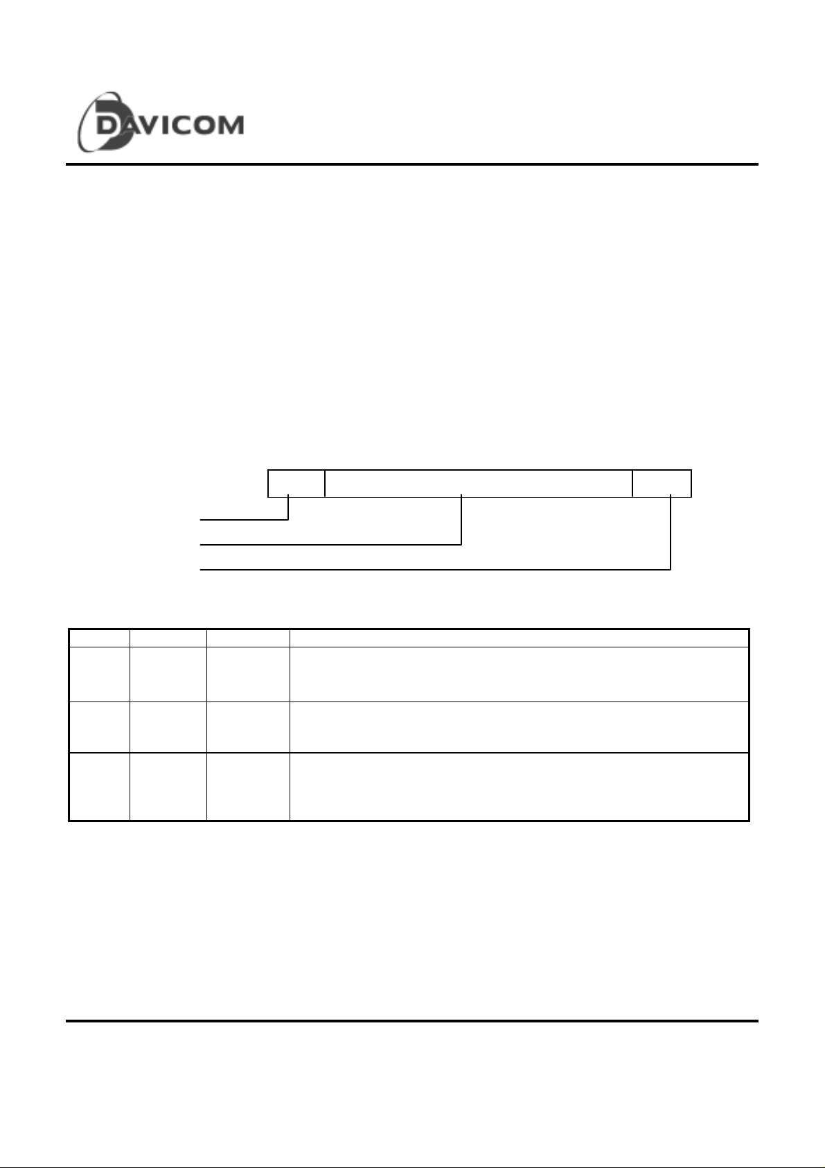
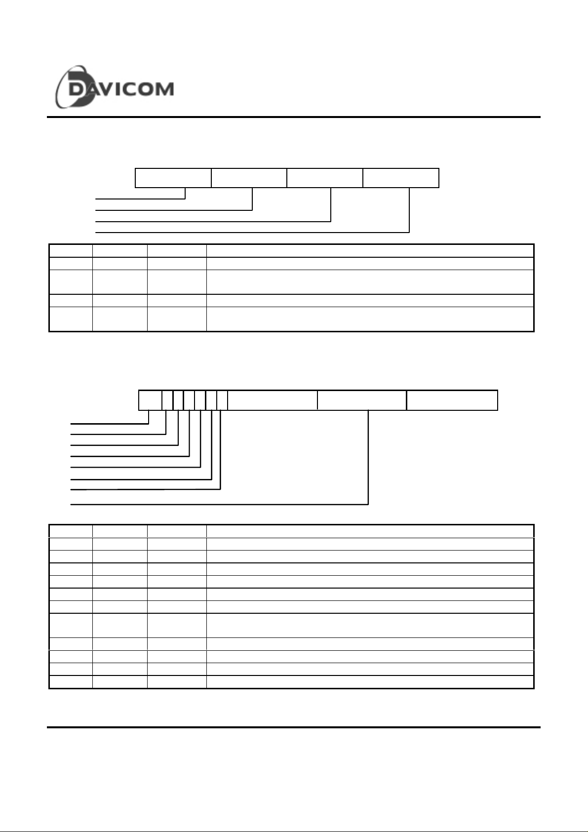
Identification ID (xxxxxx00 - PCIID)
31 16 15 0
Dev_ID
Device ID
Vendor ID
Vend_ID
Bit Default Type Description
16:31 9102h RO The field identifies the particular device. Unique and fixed number for the DM9102A
is 9102h. It is the product nu mber assigned by DAVICOM.
0:15 1282h RO This field identifies the manufacturer of the device. U nique and fixe d n umber f or
Davicom is 1282h. It is a registered number from SIG.
Command & Status (xxxxxx04 - PCICS)
31 16 15 0
Status Command
Status
Command
31 30 29 28 27 26 25 24 23 22 21 20 10
0 0 1 0 0 0191
Detected Parity Error
Signal For System Error
Master Abort Detected
Target Abort Detected
Send Target Abort
DEVSEL Timing
Data Parity Error Detected
Slave mode Fast back to Back
User Definable
66MHz Capability
New Capability
Mast Mode Fast Back-To-Back
SERR# Driver Enable/Disable
Address/Data Steeping
Parity Error Response Enable/Disable
VGA Palette snoop
Memory Write and Invalid
Special Cycle
Master Device Capability Enable/Disable
Memory Space Access Enable/Disable
I/O Space Access Enable/Disable
Reserved
98
76543210
00
00
Final 15
Version: DM9102A-DS-F03
August 28, 2000

Bit Default Type Description
31 0 R/C Detecte d Par ity Er ror
The DM9102A samples the AD[0:31], C/BE[0:3]#, and the PAR signal to
ch eck p a rity and t o se t p ar it y e r r ors. I n slav e m od e , t h e pa r i ty c heck falls
on command phase and data valid phase (IRDY# and TRDY# both
active). While in master mode, the DM9102A will check during each data
phase of a me mory read cycle for a parity erro r During a memory write
cycle, if an error occurs, the PERR# signal will be driven by the target. This
bit is set by the DM9102A and cleared by writing "1". There is no effect by
writ ing " 0" .
30 0 R/C Signal For System Error
This bit is set when the SERR# signal is driven by the DM9102A. This
system error occurs when an address parity is detected under the
condition that bit 8 and bit 6 in command register below are set.
29 0 R/C Master Abort Detected
This bit is set when the DM9102A terminates a master cycle with the
master-abort bus transaction.
28 0 R/C Target Abort Detected
This bit is set when the DM9102A terminates a master cycle due to a
target-abort signal from other targets.
27 0 R/C Send Target Abort (0 For No Implementation)
The DM9102A will never assert the target-abort sequence.
26:25 01 R/C DEVSEL Timing (0 1 Se lect Me dium T iming)
Medium timing of DEVSEL# means the DM9102A will assert DEVSEL#
signal two clocks after FRAME# is sample “asserted.”
24 0 R/C Data Pa rity Error Detec ted
This bit will take effect only when operating as a master and when a Parity
Error Response Bit in command configuration register is set. It is set under
two conditions:
(i) PERR# asserted by the DM9102A in memory data read error, (ii)
PERR# sent from the target due to memory data write error.
23 0 RO Slave mode Fast Back-To-Bac k Capable (0 For Not Support)
This bit is always reads "1" to indicate that the DM9102A is capable of
accepting fast back-to-back transaction as a slave mode device.
22 0 RO User-Definable-Feature Supported (0 For Not Support)
21 0 RO 66 MHz Capable (0 For No Capability)
20 1 RO New Capabilities (1 For Good Capability)
This bit indicates whether this function implements a list of extended
capabilities such as PCI power management. When set this bit indicates
the presence of New Capabili tie s. A val u e of 0 means that this funct ion
does not implement New Capabilities.
19:10 0 RO Reser ved
9 0 RO Master Mode Fast Back-To-Back (0 For Not Support)
The DM9102A does not support master mode fast back-to-back capability
and will not generate fast back-to-back cycles.
8 0 RW SERR# Driver Enable/Disable
This bit controls the assertion of SERR# sign al output. The SERR# output
will be asserted on detect ion o f an address parity error and if both this bit
Single Chi p Fast E thern et NIC c ont roller
DM9102A
16 Final
Version: DM9102A-DS-F03
August 28, 2000

Single Chi p Fast E thern et NIC c ont roller
and bit 6 are set.
7 0 RO Address/Data Stepping (0 For No Stepping)
6 0 RW Parity Error Response Enable/Disable
Setting this bit will enable the DM9102A to assert PERR# on the detection
of a data parity error and to assert SERR# for reporting address parity
error.
5 0 RO VGA Palette Snooping (0 For Not Support)
4 0 RO Memory Write and Invalid (0 For Not Implementation)
The DM9102A only generates Memory write cycle.
3 0 RO Special Cycles (0 For Not Implementation)
2 1 RW Master Device Capability Enable/Disable
When this bit is set, DM9102A has the a bility of master mode operation.
1 1 RW Memory Space Access Enable/Disable
This bit controls the ability of memory space acc ess. The memory access
includes memory mapped I/O access and Boot ROM access. As the
system boots up, this bit will be enabled by BIOS for Boot ROM memory
access. While in normal operation using memory mapped I/O access, this
bit should be set by driver before memory access cycles.
0 1 RW I/O Space Access Enable/Disable
This bit controls the ability of I/O space access. I t will be set by BIOS after
power on.
DM9102A
Revision ID (xxxxxx08 - PCIRV)
31
Class Code
Class Code
Revision Major Number
Revision Minor Number
Bit Default Type Description
31:8 020000h RO Class Code (020000h)
This is the standard code for Ethernet LAN controller.
7:4 0011 RO Revision Major Number
This is t he s il i co n- ma jo r r evisio n nu m ber that will increase for the subsequent
versions of the DM9102.A.
3:0 0001 RO Revision Minor Number
This is t he s il i co n- m ino r r evisio n nu m ber that will increase for the subsequent
versions of the DM9102A.
4
3
Revision ID
078
Final 17
Version: DM9102A-DS-F03
August 28, 2000

DM9102A
Miscellaneous Function (xxxxxx0c - PCILT)
31 16 15 0872324
BIST Header Type Latency Timer Cache Line Size
Built-In Self Test
Header Type
Latency Timer For The Bus Master
Cache Line Size For Memory Read
Bit Default Type Description
31:24 00h RO Built In Self Test ( 00h Means Not Implementation)
23:16 00h RO Header Type ( 00h Means single function with Predefined Header Type )
15:8 00h RW Latency Timer For The Bus Master.
The latency timer is guaranteed by the system and measured by clock cycles.
Wh e n t h e F R A M E# a s s e r t e d a t t h e b e g i n n i n g of a m a s t er pe r i o d by t he D M9102A,
the value will be copied into a counter and start counting down. If the FRAME# is
de-asserted prior to count expiration, this value is meaningless. When the count
expires before GNT# is de-asserted, the master transaction will be terminated as
soon as the GNT# is removed.
While GNT# signal is removed and the counter is non-zero, the DM9102A will
continue with its data transfers until the count expires. The system host will read
MIN_GNT and MAX_LAT registers to determine the latency requirement for the
device and then initialize the latency timer with an appropriate value.
The reset value of Latency Timer is determined by BIOS.
7:0 00h RO Cache line Size For Memory Read Mode Selection ( 00h Means Not
Implementation For Use)
Single Chi p Fast E thern et NIC c ont roller
I/O Base Address (xxxxxx10 - PCIIO)
31 0
I/O Base Address
I/O Base Address
PCI I/O Range
18 Final
I/O or Memory Space Indicator
0000000
1 7 8
1
Version: DM9102A-DS-F03
August 28, 2000

Single Chi p Fast E thern et NIC c ont roller
Bit Default Type Description
31:7 Undefined RW PCI I/O Base Address
This is the base address value for I/O accesses cycles. It w ill b e compared to
AD[31:7] in the address phase of bus command cycle for the I/O resource access.
6:1 000000 RO PCI I/O Range Indication
It indicates that the minimum I/O resource size is 80h.
0 1 RO I/O Space Or Memory Space Base Indicator
Determines that the register maps into the I/O space.( = 1 Indicates I/O Base)
Memory Mapped Base Address (xxxxxx14 - PCIMEM)
DM9102A
31
Memory Mapped
Base
Memory Base Address
Memory Range Indication
I/O or Memory Space Indicato r
8
1 7
0000000
Bit Default Type Description
31:7 Undefined R/W PCI Memory Base Address
This is the base address value for Memory accesses cycles. It will be compared to
the AD[31:7] in the address phase of bus command c ycle for the Memo ry r esource
access.
6:1 000000 RO PCI Memory Range Indication
It indicates that the mini mum Mem ory resource size is 80h.
0 0 RO I/O Space Or Memory Space Base Indicator
Determines that the register maps into the memory space( = 0 Indicates Memory
Base)
Subsystem Identification (xxxxxx2c - PCISID)
Subsystem ID Subsystem Vendor ID
Subsystem ID
Subsystem Vendor ID
0
0
031
Bit Default Type Description
31:16 XXXXh RO Subsystem ID
It can be loaded from EEPROM word 1 and different from each card.
15:0 XXXXh RO Subsystem Vendor ID
Unique number given by PCI SIG and loaded from EEPROM word 0.
Final 19
Version: DM9102A-DS-F03
August 28, 2000
CardBus CIS Pointer (xxxxxx28 - CCIS)
This Card Information Structure (CIS), also known as tuples,
is a set of data structures saved in a nonvolatile memory on
the CardBus Card. The data stored in CIS describes the
product. Included in this data are the product
manufacturer’s name, product name, and most importantly,
the hardware description. The CIS is supported in the boot
ROM space or the memory space (serial ROM).
CIS is read upon card insertion into the socket. The
software entity that traditio n all y r eads the CIS is usually
known as Card Services and Socket Se rvices (CS & SS).
8
31 03272
ROM Image
Addre ss Space Offset
DM9102A
Single Chi p Fast E thern et NIC c ont roller
The CCIS pointer register is a read-only 32-bit reg ister.
This register points to one of the possible address space
where the card information structure (CIS) begins. The
pointer is used in a CardBus environment. The content of
CCIS is loaded from the serial ROM after a hardware reset.
A value o f 0 in th is re g iste r ind ica tes tha t C IS is n ot
supported.
2
Addre ss Space Indicato r
Bit Default Type Description
31:28 Note R/W ROM Image
The 4- bi t ROM image fiel d value when the CIS reside in an expansion ROM.
27:3 Note R/W Address Space Offset
This field contains the address offset within the address space indicate d b y the
address space indicator field (CCIS<2:0>)
2:0 Note R/W Address Space Indicator
This field indicates the location of the CIS base address. The value of 2 indicates
that the CIS is stored in the serial ROM, and 7, indicates that the CIS is sto re d in the
expansion ROM.
note : read from serial ROM
20 Final
Version: DM9102A-DS-F03
August 28, 2000

Expansion ROM Base Address (xxxxxx30 - PCIROM)
DM9102A
Single Chi p Fast E thern et NIC c ont roller
31 01
ROM Base Address
ROM Base Address
18 17
11
0000000
00000000
10
9
Reserved
Bit Default Type Description
31:10 00h RW ROM Base Address With 256K Boundary
PCIROM bit17~10 are hardwired to 0, indicating ROM Size is up to 256K Size
9:1 000000000 RO Reserved Bits Read As 0
0 0 RW Expansion ROM Decoder Enable/Disable
If this bit and the memory space access bit are bot h set to 1, the DM9102A will
responds to its expansion ROM.
Capabilities Pointer (xxxxxx34 - Cap _Ptr)
31
Reserved
0
10100 00
R/W
078
Capability Pointer
Bit Default Type Description
31:8 000000h RO Reserved
7:0 01010000 RO Capability Pointer
The Cap_Ptr provides an offset (default is 50h) into the function’s PCI Configuration
Space for th e loca tion o f the f ir st t er m in th e Capabilitie s Linked List. The Cap_Ptr
offset is DOUBLE WORD aligned so the two least s ignificant bits are always “0”s
Final 21
Version: DM9102A-DS-F03
August 28, 2000
DM9102A
Interrupt & Latency Configuration (xxxxxx3c - PCIINT)
31 16 15 0872324
MAX_LAT MIN_GNT INT_PIN INT_LINE
Maximum Latency Timer
Minimum Grant
Interrupt Pin
Interrupt Line
Bit Default Type Description
31:24 28h RO Maximum Latency Timer that can be sustained (Read Only and Re ad As 28h)
23:16 14h RO Minimum Grant
Minimum Length of a Burst Period (Read Only and Read As 14h)
15:8 01h RO Interrupt Pin read as 01h to indicate INTA#
7:0 XXh RW Interrupt Line that Is Routed to the Interrupt Controller
The value depends on mainboard.
Device Specific Configuration Register (xxxxxx40h- PCIUSR)
Single Chi p Fast E thern et NIC c ont roller
3130 29 1615 8 0
Device Specific
Link Event enable/disable
Sample Frame Event enable/disable
Magic Packet Event enable/disable
Link Event Status
Sample Frame Event Status
Magic Packet Event Status
Device Specific
272628
25 24 23
Reserved
7
Reserved
Bit Default Type Description
31 0 RW Device Specific Bit (sleep mode)
30 0 RW Device Specific Bit (snooze mode)
29 0 RW When set enable Link Status Change Wake-up Event
28 0 RW When set enable Sample Frame Wake-up Event
27 0 RW When set enable Magic Packet Wake-up Event
26 0 RO When set, indicates link change and Link Status Change Event occurred
25 0 RO When set, indicates the sample frame is received and Sample Frame Event
occurred
24 0 RO Whe n s e t, i n d ic a t e s th e Ma g i c Pa c k et i s re c e i v ed and Ma g i c p a c k e t E ve n t o cc u r r e d
23:16 00h RO Reserved Bits Read As 0
15:8 00h RW Device Specific
7:0 00h RO Reserved Bits Read As 0
22 Final
Version: DM9102A-DS-F03
August 28, 2000

Power Management Register (xxxxxx50h~PCIPMR)
31 16 15 087
PM C Next Item Pointer Capability ID
Power Management Capabilities
Next Item Pointer
Capability Identifier
Bit Default Type Description
31:27 11000 RO PME_Support
These five bits field indicate the power states in which the function may assert
PME#. A value of 0 for any b it indicates that the function i s n o t c apabl e of asserting
the PME# signal while in that power state.
bit27 Æ PME# support D0
bit28 Æ PME# support D1
bit29 Æ PME# support D2
bit30 Æ PME# support D3(hot)
bit31 Æ PME# support D3(cold)
DM9102A’s bit31~27=11000 indicates PME# can be asserted from D3(hot) &
D3(cold).
26:22 00000 RO Reserved (DM9102A not supports D1, D2)
21 1 RO A “1” in d ica t es t ha t th e fun c t ion r eq u ir es a devic e sp ec ific initiali za tion sequence
following transition to the D0 uninitialized state.
20 1 RO Auxiliary Power Source
This b it is o n ly me aning ful i f bi t31 i s a “1 ” .
This bit is “1” in DM9102A indica tes that support for PME# in D3(cold) requires
auxiliary power.
19 0 RO PME# Clock
“0” indicates that no PCI clock is required for the function to generate PME#.
18:16 001 RO Version
A value of 001 indicates that this function complies with the Revision 1.0 of the PCI
Power Management Interface Specification.
A value of 010 is for DM9102A/A that complies with the revision 1.1 of the PC I
Power Management Interface Specification.
15:8 00h RO Next Item Pointer
The offset into the function’s PCI Configuration Space pointing to the location of
next item in the function’s capability list is “00h”
7:0 01h RO Capability Identifier
When “01h” indicates the linked list item as being the PCI Power Management
Registers.
Single Chi p Fast E thern et NIC c ont roller
DM9102A
Final 23
Version: DM9102A-DS-F03
August 28, 2000

Power Management Control/Status (xxxxxx54h~PMCSR)
DM9102A
Single Chi p Fast E thern et NIC c ont roller
31
0 0 0 0 0 0 0 0 0 0 0 0 0 0 0 0
PME_Status
16 15 14 9 8 7 2 1 0
R/W 0 0 0 0 0 0 R/W 0 0 0 0 0 0 R/W
PME_En
Power_State
Bit Default Type Description
31:16 0000h RO Reserved
15 0 RW/C PME_Status
This bit is set when the function would normally assert the PME# signal
independent of the state of the PME_En bit. Writing a “1” to this bit will clear it.
This bit defaults to “0” if the function does not support PME# generation from
D3(cold).If the function supports PME# from D3(cold) then this bit is sticky a n d
must be explicitly cleared by the operating sy stem each time the operating
system is initially loaded.
14:9 000000 RO Reserved.
It means that the DM9102A does not s upport reporting power consumption.
8 1 RW PME_En
Write “1” to enables the function to assert PME#, write “0” to disable PME#
assertion.
This bit defaults to “0” if the function does not support PME# generation from
D3(cold).
If the function supports PME# from D3(cold) then this bit is sticky and must be
explicitly cleared by the operating system each time the operating system is
initia lly loaded.
7:2 000000 RO Reserved
1:0 00 RW This tw o bits field is both used to d et ermine the current power sta te of a function
and to set the function into a new power state. Th e definitions given below.
00 : D0
11 : D3(hot)
24 Final
Version: DM9102A-DS-F03
August 28, 2000
 Loading...