

Davicom DM9101F, DM9101E Datasheet
DM9101
10/100Mbps Ethe rnet P hysical Layer Si ngle Chi p Transc ei ver
General Descri ption
The DM9101 is a physical-layer, single-chip, low-power
transceiver for 100Base-TX, and 10Base-T operations. On
the media side, it provides a direct interface either to
Unshielded Twisted Pair Category 5 Cable (UTP5) for
100Base-TX Fast Ethernet, or UTP5/UTP3 Cable for
10Base-T Ethernet. Through the IEEE 802.3u Media
Independent Interface (MII), the DM9101 connects to the
Medium Access Control (MAC) layer, ensuring a high interoperability among products from different vendors.
The DM9101 uses a low-power and high-performance
CMOS process. It contains the entire physical layer
functions of 100Base-TX as defined by IEEE 802.3u,
including the Physical Coding
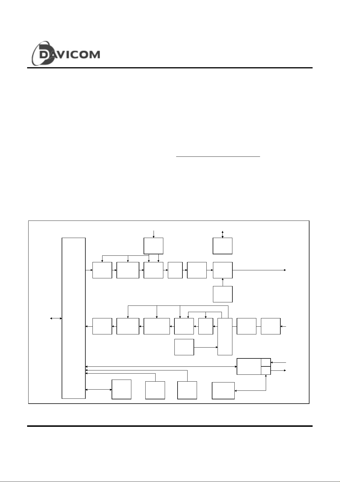
Block Diagram
TX CGM
Sublayer (PC S), Physi cal Me diu m A ttachmen t (PMA),
100Base-TX Twisted Pair Physical Medium Dependent
Sublayer (TP-PMD), and a 10Base-T Encoder/Decoder
(ENC/DEC). The DM9101 provides strong support for the
Auto-negotiation function utilizing automatic media speed
and protocol selection. The DM9101 incorporates an
internal wave-shaping filter to control rise/fall time,
el i m i n a t in g t h e need fo r e x t e rn al f i l te rin g o n the 10/100Mbps
signals.
Patent-Pending Circuitry Includes:
Smart adaptive receiver equalizer
Digital algorithm for high frequency clock/data recovery
circuit
High speed wave-shaping circuit
LED1-4#25M OSCI
LED
Driver
NRZ
to
NRZI
25M CLK
Serial to
Parallel
Digital
Logic
Carrier
Sense
NRZI to
MLT-3
125M CLK
NRZI
to
NRZ
MLT-3
Driver
Rise/Fall
Time
CTL
RX
CRM
Auto-
Negotiation
MLT-3 to
NRZI
10BASE-T
Module
Adaptive
EQ
RX
TX
100TXD+/-
RXI+/-
RXI+/10TXD+/-
MII
Signals
MII
Interface/
Control
4B/5B
Encoder
4B/5B
Decoder
Scrambler
Codegroup
Alignment
Register
Parallel
to Serial
Descrambler
Collision
Detection
Final 1
Version: DM9101 - DS -F03
July 22, 1999
Table of Contents
DM9101
10/100Mbps Ethe rnet P hysical Layer Si ngle Chi p Transc ei ver
General Descri pti on................................................1
Block Diagram........................................................1
Features.................................................................3
Pin Configuration: DM9101E LQFP.........................3
Pin Configuration: DM9101F QFP...........................4
Pin Description .......................................................5
Functional Descr i pti on
MII Inter fa ce......................................................12
100Base-TX Operat ion......................................14
100Base-TX Transm it........................................14
100Base-TX Operat ion......................................15
4B5B Encoder ...................................................15
Scrambler..........................................................15
Paralle l to Serial Converter................................15
NRZ to NRZI Encoder........................................15
MLT-3 Converter ...............................................15
MLT-3 Driver .....................................................15
4B5B Code Group .............................................16
100Base-TX Receiver........................................17
Signal Detect.....................................................17
Digital Adaptive Equalization..............................17
MLT-3 to NRZI Decoder.....................................17
Clock Recovery Module.....................................18
NRZI to NRZ .....................................................18
Serial to Parallel................................................18
Descrambler......................................................18
Code Group Alignment ......................................18
4B5B Decoder...................................................18
10Base-T Operation..........................................18
Collisio n Detection.............................................18
Carrier Sense....................................................18
Auto-Negotiation................................................18
MII Serial Management......................................19
Serial Management Inter face.............................19
Management Interface – Read Frame Structure.19
Management Interface – Write Frame Structure.19
Register Description .............................................20
- Key To Default....................................................20
- Register 2 ..........................................................23
PHY ID Identifier Register #2 (PHYIDR2)
- Register 3 ..........................................................24
Auto-negotiation Advertisement Register (ANAR)
- Register 4 ..........................................................24
Auto-negotiation Link Partner Ability Register
(ANLPAR) - Register 5 .........................................25
Auto-negotiation Expansion Register (ANER)
- Register 6 ..........................................................26
DAVICOM Specified Configuration Register (DSCR)
- Register 16.........................................................26
DAVICOM Specified Configuration and Status
Register (DSCSR) - Register 17 ...........................28
10Base-T Configuration / Status (10BTS CRCS R)
- Register 18.........................................................29
Abso lu te Maximum Ratings..................................30
DC Electrical Characteristics ................................31
AC Characteristics................................................32
Timing Waveforms
MII-100Base-T X Tr ansmit Timing Diagram........33
MII-100Base-TX Receive Timing Diagram.........33
Auto-negotiation and Fast Link Pulse Timing.....34
MII-10Ba se-T Transmit Tim ing Diagram............35
MII-10Base-T Receive Nibble Timing Diagram ..35
10BASE-T SQE (Heartbeat) Timing Diagram.....36
10BASE-T Jab and Unjab Timing Diagram........36
MDIO Timing when OUTPUT by STA................37
MDIO Timing when OUTPUT by DM9101..........37
Magnetics Selection Guide...................................38
Crystal Selection Guide........................................38
Application Circuit (for reference only) ..................40
Basic Mode Control Register (BMCR)
- Register 0...........................................................21
Basic Mode Status Register (BMSR)
- Register 1...........................................................22
PHY ID Identifier Register #1 (PHYIDR1)
2 Final
Package Information.............................................41
Ordering Information.............................................42
Company Overview..............................................42
Contact Windows..................................................42
Version: DM9101 - DS -F03
July 22, 1999

10/100Mbps Ethe rnet P hysical Layer Si ngle Chi p Transc ei ver
Features
• 10/100Base-TX physical-layer, single-chip transceiver
• Compliant with IEEE 802.3u 100Base-TX standard
• Compliant with ANSI X3T12 TP-PMD 1995 standard
• Compliant with IEEE 802.3u Auto-negotiation protocol
for a uto m at ic lin k typ e s e lec t ion
• Supports the MII with serial management interface
• Supports Full Duplex operation for 10 and 100Mbps
• High performance 100Mbps clock generator and data
recovery circuitry
• Adaptive equalization circuitry for 100Mbps receiver
Pin Configu ration: DM9101E LQFP
AGND
AGND
NC
AVCC
10BTSER
BPSCR
BP4B5B
BPALIGN
RPTR/NODE#
OPMODE3
OPMODE2
OPMODE1
OPMODE0
PHYAD4
DM9101
• Controlled output edge rates in 100Mbps
• Supports a 10Base-T interface without the need for
an external filter
• Provides Loop-back mode for system diagnostics
• Includes Flexible LED configuration capability
• Dig ita l clo c k r ec o ver y c irc u it us in g advance d digit al
algorithm to reduce jitter
• Low-power, high-performance CMOS process
• Available in both a 100 pin LQFP and a 100 QFP
package
PHYAD3
DGND
DVCC
PHYAD2
PHYAD1
PHYAD0
TESTMODE
RESET#
RX_ER/RXD4
RX_EN
RX_DV
NC
NC
NC
AGND
AVCC
AVCC
RXI-
RXI+
AGND
AGND
10TXO-
10TXO+
AVCC
AVCC
AGND
AGND
NC
NC
AVCC
AVCC
AGND
AGND
100TXO-
100TXO+
AVCC
11
18
1
2
4
7
8
9
10
12
13
14
15
16
17
19
20
21
22
23
24
25
8
99
98
97
100
3
5
6
96959493929190898887868584
DM9101E
26
27
3031323334353738394041
28
AVCC
OSCI/X1
29
X2
AGND
AVCC
AGND
BGREF
OSC/XTL#
36
DGND
DGND
BGRET
DVCC
DGND
UTP
TRIDRV
SPEED10
42
RX_LOCK
1
82
NC
LINKSTS
797877
80
DVCC
CLK25M
FDXLED#
COLLED#
83
43444546474849
DGND
76
75
74
73
72
71
70
69
68
67
66
65
64
63
62
6
1
60
59
58
57
56
55
54
53
52
5
1
50
DGND
COL
CRS
RX_CLK
DVCC
DGND
RXD0
RXD1
RXD2
RXD3
DVCC
DGND
MDIO
MDC
TX_CLK
TX_EN
DVCC
DGND
TXD0
TXD1
TXD2
TXD3
TX_ER/TXD4
TXLED#
RXLED#
LINKLED#
Final 3
Version: DM9101 - DS -F03
July 22, 1999

Pin Configu ration: DM9101 F QFP
DM9101
10/100Mbps Ethe rnet P hysical Layer Si ngle Chi p Transc ei ver
AVCC
NC
NC
NC
NC
AGND
AVCC
RXI-
RXI+
AGND
AGND
10TXO-
10TXO+
AVCC
AVCC
AGND
AGND
NC
NC
AVCC
AVCC
AGND
AGND
100TXO-
100TXO+
AVCC
AVCC
OSCI/X1
X2
1
2
3
4
5
6
7
8
9
10
11
12
13
14
15
16
17
18
19
20
21
22
23
24
25
26
27
28
29
30
AGND
AGND
99
100
32
31
BP4B5B
BPSCR
10BTSER
96
97
98
35
34
33
OPMODE3
RPTR/NODE#
BPALIGN
93
94
95
OPMODE2
92
91
90
PHYAD4
89
OPMODE0
OPMODE1
DM9101F
36
37
38
39
424041
DVCC
PHYAD3
87
88
44
43
PHYAD2
DGND
85
86
46
45
PHYAD0
PHYAD1
83
84
48
47
RESET#
TESTMODE
81
82
80
79
78
77
76
75
74
73
72
71
70
69
68
67
66
65
64
63
62
61
60
59
58
57
56
55
54
53
52
51
50
49
RX_EN
RX_ER/RXD4
RX_DV
COL
CRS
RX_CLK
DVCC
DGND
RXD0
RXD1
RXD2
RXD3
DVCC
DGND
MDIO
MDC
TX_CLK
TX_EN
DVCC
DGND
TXD0
TXD1
TXD2
TXD3
TX_ER/TXD4
TXLED#
RXLED#
LINKLED#
DGND
COLLED#
AGND
OSC/XTL#
AVCC
AGND
BGRET
BGREF
DGND
DGND
DVCC
DGND
UTP
TRIDRV
SPEED10
NC
DGND
RX_LOCK
CLK25M
LINKSTS
DVCC
FDXLED#
4 Final
Version: DM9101 - DS -F03
July 22 , 1 999

Pin Descr iption
Pin No. Pin Name I/O Description
LQFP QFP
MII Interface
54 56 TX_ER/
TXD4
DM9101
10/100Mbps Ethe rnet P hysical Layer Si ngle Chi p Transc ei ver
Transmit Error:
I
In 100Mbps mode, if this signal is asserted high and TX_EN is
active, the HALT sym bol is substituted for the actual data nibble.
In 10Mbps mode, this input is ignored.
In bypass modes (BP4B5B or BPALIGN), TX_ER becomes the
TXD4 pin, the fifth TXD data bit.
55-58 57 - 60 TXD3
TXD2
TXD1
TXD0
61 63 TX_EN I
62 64 TX_CLK O,Z
63 65 MDC I
64 66 MDIO I/O
67-70 69 - 72 RXD3
RXD2
RXD1
RXD0
73 75 RX_CLK O,Z
I
O,Z
Transmit Data:
Transmit data input pins for nibble data from the MII in 100Mbps
or 10Mbps nibble mode (25 MHz for 100Mbps mode, 2.5MHz for
10Mbps nibble mode) .
In 10Mbps serial mode, the TXD0 pin is used as the serial data
input pin. TXD[3:1] are ignored.
Transmit Enable:
Active high input indicates the presence of valid nibble data on
TXD[3:0] for both 100Mbps or 10Mbps nibbl e mode.
In 10Mbps serial mode, active high indicates the pres ence of
valid 10Mbps data on TXD0.
Transmit Clock:
Transmit c lock output from the DM9101:
- 25MHz nibble transmit clock derived from transmit Phase
Locked Loop(TX PLL) in 100Base-TX mode
- 2.5MHz transmit clock in 10Base-T nibble mode
- 10MHz transmit clock in 10Base-T serial mode
Management Data Clock:
Synchronous clock to the MDIO management data input/output
serial interface which is asynchronous to transmit and receive
clocks. The maximum clock rate is 2.5MHz.
Management Data I/O:
Bi-directional management instruction/data signal that may be
driven by the station management entity or the PHY. This pin
requires a 1.5KΩ pull-up resistor.
Receive Data:
Nibble wide receive data (synchronous to RX_CLK - 25MHz for
100Base-TX mode, 2.5MHz for 10Base-T nibble mode). Data is
driven on the falling edge of RX_CLK.
In 10Mbps serial mode, the RXD0 pin is used as the data output
pin. RXD[3:1] are ignored.
Receive Clock:
Provides the recover ed receiv e clock for diff er ent modes of
operation:
- 25MHz nibble clock in 100Mbps mode
- 2.5MHz nibble clock in 10Mbps nibble mode
- 10MHz receive clock in 10Mbps serial mode
Final 5
Version: DM9101 - DS -F03
July 22, 1999

Pin Descr iption
Pin No. Pin Name I/O Description
LQFP QFP
MII Interface (continued)
74 76 CRS O,Z
75 77 COL O,Z
76 78 RX_DV O,Z
77 79 RX_ER/
78 80 RX_EN I
Media Interface
7, 8 9, 10 RXI-, RXI+ I
11, 12 13, 14 10 TXO-,
23, 24 25, 26 100 T XO - ,
(continued)
RXD4
10 TXO+
100 TXO+
O,Z
O
O
DM9101
10/100Mbps Ethe rnet P hysical Layer Si ngle Chi p Transc ei ver
Carrier Sense:
This pin is asserted high to indicate the presence of carrier due to
receive or transmit activities in 10Base-T or 100Base-TX Half
Duplex modes.
In Repeater, when Full Duplex or Loop-back mode is a logic 1, it
indicates the presence of carrier due only to receive a ctivity.
Collision Detect:
Asserted high to indicate detection of collision conditions in
10Mbps and 100Mbps Half Duplex modes. In 10Base-T Half
Duplex mode with Heart beat set active (bit 13, regi ster 18h) , it is
also asserted for a duration of approximately 1ms at the end of
transmission to indicate heartbeat. In F ull Duplex mode, this signal
is always logic 0. There is no heartbeat function in Full-Duplex
mode.
Receive Data Valid:
Asserted high to indicate that valid data is present on RXD[3:0].
Receive Error:
Asserted high to indicate that an invalid symbol has been detected
inside a received packet in 100Mbps mode.
In a bypass mode (BP4B5B or BPALIGN modes), RX_ER
becomes RXD4, the fifth RXD data bit of the 5B symbols.
Receive Enable:
Active high enabled for receive signals RXD[3:0], RX_CLK,
RX_DV and RX_ER. A low on this input tri-states these output
pins. For normal operation in a NODE application, this pin should
be pulled high.
100/10Mbps Differential Input Pair:
These pins are the differential receive input for 10Base-T and
100Base-TX. They are capable of receiving 100Base-TX MLT-3 or
10Base-T Manchester encoded data.
10Base-T Differential Output Pair:
This output pair provides controll ed rise and fall times designed to
filter the tr ansmitters output.
100Base-TX Differential Output Pair:
This output pair driv es MLT - 3 encoded data to the 100M twist ed
pair interface and provides controlled rise and fall times designed
to filter the transmitter output, reducing any associated EMI.
6 Final
Version: DM9101 - DS -F03
July 22, 1999

DM9101
10/100Mbps Ethe rnet P hysical Layer Si ngle Chi p Transc ei ver
Pin Descr iption
Pin No. Pin Name I/O Description
LQFP QFP
LED Interface :
These outputs can dire c t ly drive LE Ds or provide status information to a network management device.
48 50 FDXLED#
49 51 COLLED# O
51 53 LINKLED#
52 54 RXLED# OD
53 55 TXLED# OD
Device Configuration/Control/Status Interface
40 42 UTP O
41 43 SPEED10 O
42 44 RX_LOCK O
45 47 LINKSTS O
(continued)
(POLLED)
(TRAFFIC
LED)
Polarity/Full Duplex LED:
O
Indicates Full Duplex mode status for 100Mbps and 10Mbps
operation (Active low). If bit 4 of Register 16 (FDXLED_MODE) i s
set, the FDXLED# pin function will change to indicate the Polarity
status for 10Mbps operation. If polarit y is inver ted, the POLLED
will go ON.
Collisi on LE D :
Indicates the presence of collision activit y fo r 10 Mbps and
100Mbps operation. This LED has no meaning for 10Mbps or
100Mbps Full Duplex operation (Active low).
Link LE D:
O
Indicates Good Link stat us for 10Mbps and 100Mbps operation
(Active low).
It functions as the TR A FFIC L ED when bit 5 of register 16 is set
to 1. In TRAFFIC LED mode, it is always ON when the link is OK.
The TRAFFIC LED flashes when transmitting or receiving.
Receive LED:
Indicates the presence of receive activity for 10Mbps and
100Mbps operation (Active low).
The DM9101 incorporates a "monostable" function on the RXLED
output. This ensures that even minimal r ec eiv e activity will
generate an adequate LED ON time.
Transmit LED:
Indicates the presence of transmit activity for 10Mbps and
100Mbps operation (Active low).
The DM9101 incorporates a "monostable" function on the TXLED
output. This ensures that even minimal transmit activity will
generate an adequate LED ON time.
UTP Cable Indication:
UTP=1: Indicates UTP cable is used.
Speed 10Mbps:
When set high, this bit indicates a 10Mbps operation, when set
low 100Mbps operati on. This pin can drive a low current LED to
indicate that 100Mbps operation is selected.
Lock for Clock/Data Recovery PLL:
When this pin is high i t indicates that the receiver recovery PLL
logic has locked to the input data stream.
Link Status Register Bit:
This pin reflects the status of bit 2 register 1.
Final 7
Version: DM9101 - DS -F03
July 22, 1999

10/100Mbps Ethe rnet P hysical Layer Si ngle Chi p Transc ei ver
Pin Descr iption
Pin No. Pin Name I/O Description
LQFP QFP
Device Configuration/Control/Status Interface (continued)
88-91 90 - 93 OPMODE0
(continued)
OPMODE1
OPMODE2
OPMODE3
OPMODE0 - OPMODE3:
I
These pins are used to control the forced o r advertised operating
mode of the DM9101 (see table below). The value is latched into
the DM9101 registers at power-up/reset.
OPMODE3 OPMODE2 OPMODE1 OPMODE0 Function
0 0 0 0 Auto-neg enable
0 0 0 1 Auto-neg enable
0010Auto-neg 100TX
0011Auto-neg 100TX
0 1 0 0 Auto-neg 10TP
0 1 0 1 Auto-neg 10TX
0 1 1 0 Manual select
0 1 1 1 Manual select
1 0 0 0 Manual select
1 0 0 1 Manual select
DM9101
with all
capabilities with
Flow Control
without all
capabilities
without Flow
Control
FDX with Flow
Control onl y
FDX/HDX
without Flow
Control
FDX with Flow
Control onl y
FDX/HDX
without Flow
Control
100TX FD X
100TX HD X
10TX FDX
10TX HDX
92 94 RTPR/NOD
E#
Repeater/Node Mode:
I
When set high, this bit selects REPEATER mode; when set low, it
selects NODE. In REPEATER mode or NODE mode with Full
Duplex configured, the Carrier Sense (CRS) output from the
DM9101 will be asserted only during receive activity. In NODE
mode or a mode not configured for Full Duplex operation, CRS will
be asserted during receive or transmit activity. At power-up/reset,
the value on this pin is latched into Register 16, bit 11.
93 95 BPALIGN I
Bypass Alignment:
Allows 100Mbps transmit and receive data streams to bypass all
of the transmit and receive operations when set high.
At power-up/reset, the value on this pin is latched into bit Register
16 ,bit 13.
8 Final
Version: DM9101 - DS -F03
July 22, 1999

10/100Mbps Ethe rnet P hysical Layer Si ngle Chi p Transc ei ver
Pin Descr iption
Pin No. Pin Name I/O Description
LQFP QFP
Device Configuration/Control/Status Interface (continued)
94 96 BP4B5B I
95 97 BPSCR I
96 98 10BTSER I
(continued)
Bypass 4B5B Encoder/Decoder:
Allows 100Mbps transmit and receive data streams to bypass the
4B to 5B encoder and 5B to 4B decoder circuits when set high
At power-up/reset, the value on this pin is latched into Register
16, bit 15.
Bypass Scrambler/Descrambler:
Allows 100Mbps transmit and receive data streams to bypass the
scrambler and descrambler circuits when set high.
At power-up/reset, the value on this pin is latched into Register
16, bit 14.
Serial/Nibble Select:
10Mbps Serial Operation:
When set high, this input selec ts a serial data transfer mode.
Manchester encoded transmit and receive data is exchanged
serially with a 10MHz clock rate on the least significant bits of the
nibble-wide MII data buses, pin TXD[0] and RXD[0] respectively.
This mode is intended for use with the DM9101 connected to a
device (MAC or Repeater) that has a 10Mbps serial interface.
Serial operation is not supported in 100Mbps mode. For
100Mbps, this input is ignored.
DM9101
Clock Interface
27 29 OSCI/X1 I
28 30 X2 O
30 32 OSC/XTL# I
46 48 CLK25M O,Z
10 and 100Mbps Nibble Operation:
When set low, this input selects the MII c om pliant nibble data
transfer mode. Transmit and receive data is exchanged in nibbles
on the TXD[3:0] and RXD[3:0] pins respectively.
At power-up/reset, the value on this pin is latched into Register
18, bit 10.
Cryst al or Oscillator Input:
This pin should be connected to a 25MHz (±50 ppm) crystal if
OSC/XTL#=0 or a 25MHz (±50ppm) external TTL oscillator input,
if OSC/XTLB=1.
Crystal Oscillat or Output:
An external 25MHz (±50 ppm) crystal should be connected to th is
pin if OSC/XTL#=0, or left unconnected if OSC/XTL#=1.
Cryst al or Oscillator Selec t or Pin:
OSC/XTL#=0: An external 25MHz (±50ppm) crystal should be
connected to X1 and X2 pins.
OSC/XTL#=1: An external 25MHz (±50ppm) oscillator should be
connected to X1 and X2 should be left
unconnected.
25MHz Clock Output:. This clock is derived directly from the
crystal circuit.
Final 9
Version: DM9101 - DS -F03
July 22, 1999

DM9101
10/100Mbps Ethe rnet P hysical Layer Si ngle Chi p Transc ei ver
Pin Descr iption
Pin No. Pin Name I/O Description
LQFP QFP
PHY Address Interface:
PHYAD[4:0] provides up to 32 unique PHY address. An address selection of all zeros (00000) will result in a
PHY isolation condition. See the isolate bit description in the BMCR, address 00.
81 83 PHYAD0 I
82 84 PHYAD1 I
83 85 PHYAD2 I
86 88 PHYAD3 I
87 89 PHYAD4 I
Miscellaneous
1-3,
17, 18,
44,
100
33 35 BGREF I
34 36 BGRET I
39 41 TRIDRV I
79 81 RESET# I
80 82 TESTMODE I
2 - 5,
19, 20,
46
(continued)
NC
PHY Address 0:
PHY address bit 0 for mult iple PH Y address applications. The
status of this pin is latched into Register 17, bit 8 duri ng power
up/reset.
PHY Address 1:
PHY address bit 1 for mult iple PH Y address applications. The
status of this pin is latched into Register 17, bit 7 duri ng power
up/reset.
PHY Address 2:
PHY address bit 2 for mult iple PH Y address applications. The
status of this pin is latched into Register 17, bit 6 duri ng power
up/reset.
PHY Address 3:
PHY address bit 3 for mult iple PH Y address applications. The
status of this pin is latched into Register 17, bit 5 duri ng power
up/reset.
PHY Address 4:
PHY address bit 4 for mult iple PH Y address applications. The
status of this pin is latched into Register 17, bit 4 duri ng power
up/reset.
No Connect:
Leave these pins unconnected (floating).
Bandgap Voltage Reference:
Connect a 6.01KΩ, 1% resistor between this pin and the BGRET
pin to provide an accurate current reference for the DM9101.
Bandga p Voltage Reference Retur n:
Return pin for 6.01KΩ resistor connection.
Tri-state Digital Output Pins:
When set high, all digital output pins are set to a high impedance
state, and I/O pins, go to input mode.
Reset: Active Low input that initializes the DM9101. It should
remain low for 30ms after VCC has stabilized at 5Vdc (normal)
before it transitions high.
Test Mode Control Pin:
TESTMODE=0: Normal operating mode.
TESTMODE=1: Enable test mode.
10 Final
Version: DM9101 - DS -F03
July 22, 1999

DM9101
10/100Mbps Ethe rnet P hysical Layer Si ngle Chi p Transc ei ver
Pin Descr iption
Power a nd Ground Pins :
The power (VCC) and ground (GND) pins of the DM9101 are grouped in pairs of two categories - Digital
Circuitry Power/Ground Pairs and Analog Circuitry Power/Ground Pair.
Pin No. Pin Name I/O Description
LQFP QFP
Group A - Digital Supply Pairs
35, 36,
37, 43,
50, 59,
65, 71,
84
Group A - Digital Supply Pairs (continued)
38, 47,
60, 72,
66, 85
Group B - Analog Circuit Supply Pairs
4, 9,
10, 15,
16, 21,
22, 29,
32, 97,
98
5, 6,
13, 14,
19, 20,
25, 26,
31, 99
6, 11, 12,
27, 28, 33
37, 38,
39, 45,
52, 61,
67, 73,
86
40, 49,
62, 74,
68, 87
18, 17,
23, 24,
31, 34,
99, 100
1, 7, 8,
15, 16,
21, 22,
(continued)
DGND P Digital Logic Ground.
DVCC P Digital Logic power supply
AGND P Analog circuit ground
AVCC P Analog circuit power supply
Final 11
Version: DM9101 - DS -F03
July 22, 1999

DM9101
10/100Mbps Ethe rnet P hysical Layer Si ngle Chi p Transc ei ver
Functional D escrip tion
The DM9101 Fast Ethernet single-chip transceiver,
provides the functionality as specified in IEEE 802.3u,
integrates a complete 100Base-TX module and a
complete 10Base-T module. The DM9101 provides a
Media Independent Interface (MII) as defined in the IEEE
802.3u standard (Clause 22).
MII Interface
Carrier
Sense
The DM9101 performs all PCS (Physical Coding
Sublayer), PMA (Physical Media Access), TP-PMD
(Twisted Pair Physical Medium Dependent) sublayer,
10Base-T Encoder/Decoder, and Twisted Pair Media
Access Unit (TPMAU) functions. Figure 1 show s the major
functional blocks implemented in the DM9101.
100Base-TX
Transmitter
100Base-TX
Receiver
10Base-T
Tranceiver
Collision
Detection
Auto
Negotiation
MII Serial
Management
Interface
MII Interface
The DM 9101 provides a Media Independent Int erfa ce (M II)
as defined in the IEEE 802.3u standard (Clause 22).
The purpose of the MII interface is to provide a simple, easy
to implement connection between the MAC Reconcilia tio n
layer and the PHY. The MII is designed to make the
differences between various media transparent to the MAC
sublayer.
The MII consists of a nibble wide receive data bus, a n ibble
wide transmit data bus, and control signals to facilitate d ata
transfers between the PHY and the Reconciliation layer.
Figure 1
• TXD (transmit data) is a nibble (4 bits) of da ta that are
driven by the reconciliation sublayer synchronously with
respect to TX_CLK. For each TX_CLK period which
TX_EN is asserted, TXD (3:0) are accepted for
transmission by the PHY.
• TX_CLK (transmit clock) output to the MAC
reconciliation sublayer is a continuous clock that
provides the timing reference for the transfer of the
TX_EN, TXD, and TX_ER signals.
• TX_EN (transmit enable) input from the MAC
reconciliation sublayer to indicate nibbles are being
presented on the MII for transmission on the physical
medium.
12 Final
Version: DM9101 - DS -F03
July 22, 1999
DM9101
10/100Mbps Ethe rnet P hysical Layer Si ngle Chi p Transc ei ver
• MII Interface (continued)
• TX_ER (transmit coding error) transitions
synchronously with respect to TX_CLK. If TX_ER is
asserted for one or more clock peri ods, and TX_EN is
asserted, the PHY will emit one or more symbols that
are not part of the valid data delimiter set somewhere in
the frame being transmitted.
• RXD (receive data) is a nibble (4 b its) of data that are
sampled by the reconciliation sublayer synchronously
with respect to RX_CLK. For each RX_CLK period
which RX_DV is asserted, RXD (3:0) are trans ferred
from the PHY to the MAC reconciliation s ublayer.
• RX_CLK (receive clock) output to the MAC
reconciliation sublayer is a continuous clock that
provides the timing reference for the transfer of the
RX_DV, RXD, and RX_ER signals.
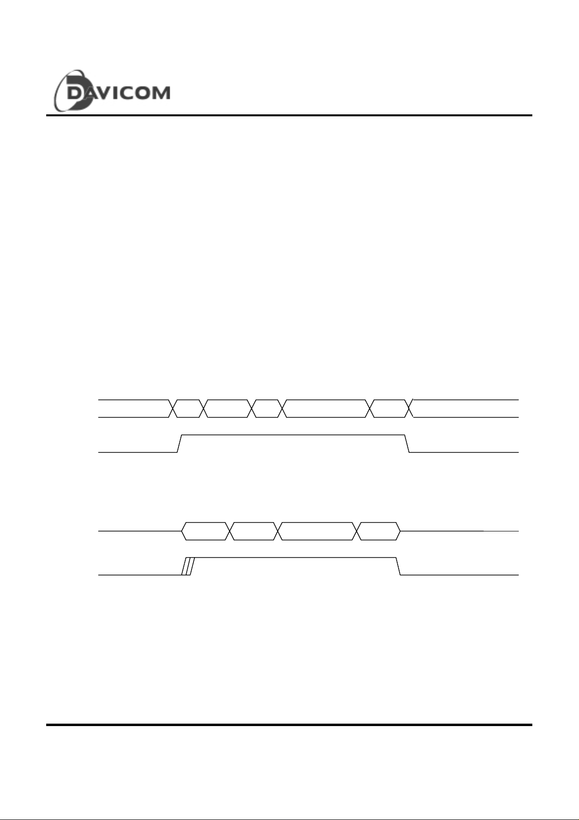
TXD
IDLE
SSD
J/K
Preamble
SFD
• RX_DV (receive data v alid) input from the PHY to
indicate the PHY is presenting recovered and decoded
nibbles to the MAC reconciliation sublayer. To interpret
a receive frame correctly by the reconciliation sublayer,
RX_DV must encompass the frame starting no later
than the Start-of-Frame delimiter and excluding any
End-Stream delimiter.
• RX_ER (receive error) transiti ons synchronously with
respect to RX_CLK. RX_ER will be asserted for 1 or
more clock periods to indicate to the reconciliation
sublayer that an error was detected somewhere in the
frame being transmitted from the PHY to the
reconciliation sublayer.
• CRS (carrier sense) is asserted by the PHY when
either the transmit or receive medium is non-idle and
deasserted by the PHY when the transmit and rece ive
mediu m are id le. Figure 2 d epi cts the beha vior of CRS
during 10Base-T and 100Base-TX transmission.
Data
ESD
T/R
IDLE
CRS
TXD
CRS
Preamble SF D
100Base-TX
10Base-T
Figure 2
Data
EFD
Final 13
Version: DM9101 - DS -F03
July 22, 1999
 Loading...