

Davicom DM9008F Datasheet
General Descriptio n
DM9008
ISA/Plug & Play Super Ethernet Contoller
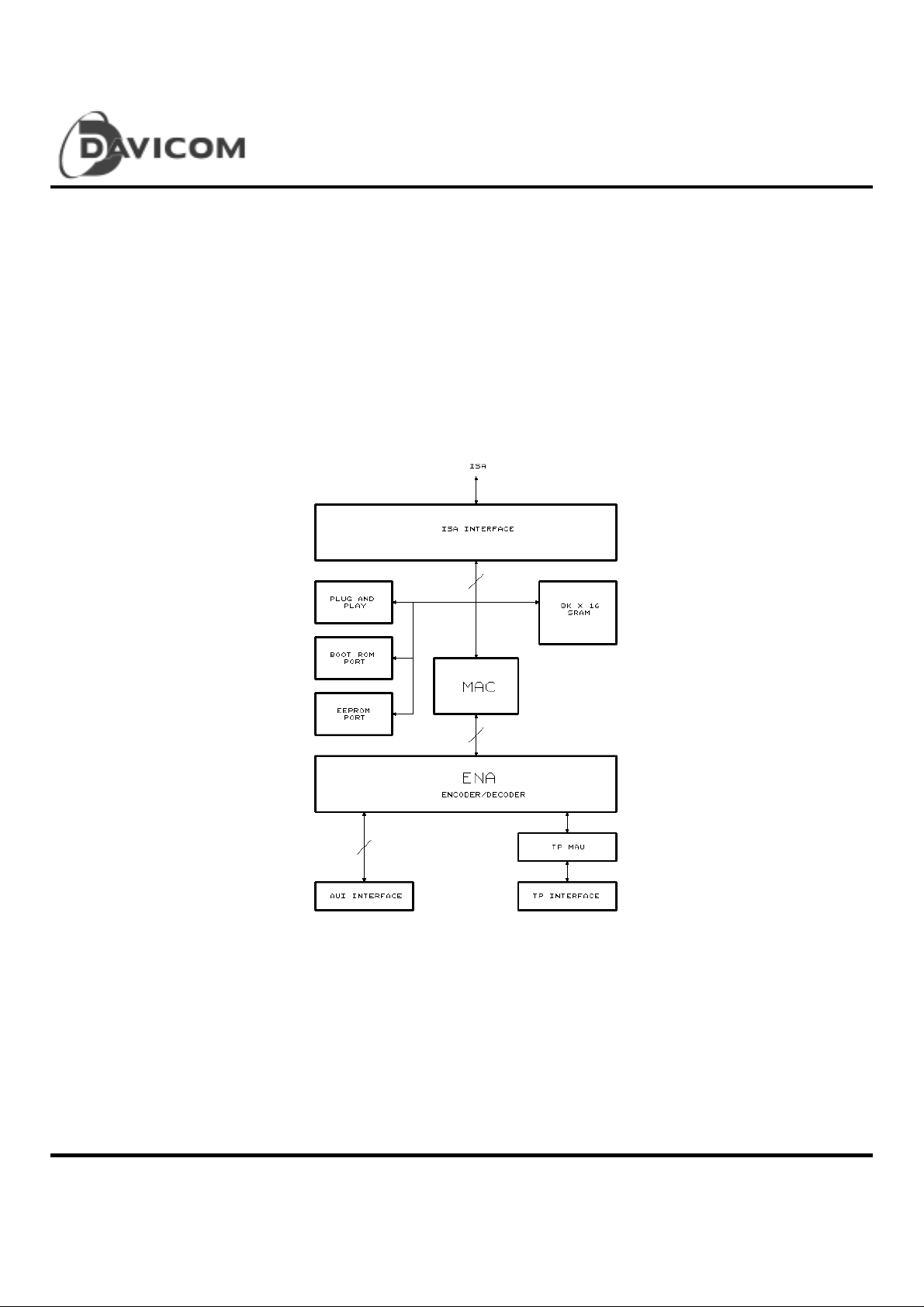
The DM9008 Ethernet controller is a highly integrated design
that provides all Medial Access Control (MAC)
and Encode-Decode (ENDEC) functions in accordance with
the IEEE 802.3 standard. Network interfaces
include 10BASE5 or 10BASE2 Ethernet via the AUI
port and 10BASE-T via the Twisted-pair. The DM9008
Ethernet controller can interface directly to the PC-AT
ISA bus without any external device. The interface to
PC-AT ISA bus is fully compatible with NE2000 Ethernet
Block Diagram
adapter cards, so all software programs designed for NE2000
can run on the DM9008 card without any modification.
Microsoft's Plug and Play and the jumperless software
configuration function are both suppo rted. The capab ility o f the
PnP and Non-PnP mode auto-switch function allows users to
con f igur e network card . No jumpers or swit ches ar e needed to
set when using either the PC
or PnP function. The integrated 8Kx16 SRAM and 10BASE-T
tr ansceiver make D M9008 more co s t-effective .
Final 1
Version :D M 90 08-DS-F02
June 14, 2000
Features
Single chip solution for IEEE 802.3, 10BASE-T,
10BASE2 and 10BASE5
Integrated ISA interface, 8Kx16 SRAM, Media Access
Control, ENDEC and 10BASE-T transceiver
Supports ISA Plug and Play configuration
Software-compat ible w i th NOVELL NE2000
Supports PnP and Non-PnP Auto-switching
PnP, Non-PnP and Auto-switch mode software
selectable
8 interrupt lines selectable
Auto-Polarity detection and correction
Selectable 8 and 16-bit slot mode
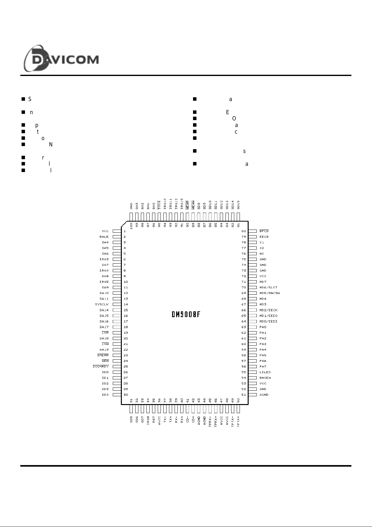
Pin Co nfigurati o n
DM9008
ISA/Plug & Play Super Ethernet Contoller
Provides auto-detection/auto-switching for 10BASE-T
Transceiver and Attachment Unit Interface (AUI)
External EEPROM programmable
Supports BOOT-ROM page mode
Loopback capability for diagnostics
Receiver and collision squelch circuit to reduce noise
Low-power CMOS process with single 5V power
supply
Built-in pre-distortion resisters for 10BASE-T
application
100-pin QFP package
2 Final
Version :D M 90 08-DS-F02
June 14, 2000
Absolute Maximum Ratings*
DM9008
ISA/Plug & Play Super Ethernet Contoller
*Comments
Supply Voltage (VCC) . . . . . . . . . . . . . . . . -0.5V to +7.0V
DC Input Voltage (Vin) . . . . . . . . . . . -0.5V to VCC +0.5V
DC Output Voltage (Vout) . . . . . . . . . -0.5V to VCC +0.5V
Storage Temperature Range (Tstg) . . . -65°C to + 150°C
Power Dissipation (PD) . . . . . . . . . . . . . . . . . . . . 500 mW
Lead Temp. (TL) (Soldering, 10 sec.) . . . . . . . . . . 235°C
Case Temp. (Tc) . . . . . . . . . . . . . . . . . . . . . . 0°C to 85°C
ESD rating (Rzap = 1.5k, Czap = 120 pF) . . . . . . . 4000V
Differential Input Voltage . . . . . . . . . . . . . . . -5.5V to 16V
Differential Output Voltage . . . . . . . . . . . . . . . . 0V to 16V
DC Electrical Characteristics
Symbol Parameter Min. Max. Unit Conditions
Voh High Level Output Voltage
(Notes 1, 2)
Vol Low Level Output Voltage
(Notes 1, 2)
Vih High Level Input Voltage (Note 6) 3.0 V
Vil Low Level Input Voltage (Note 6) 0.8 V
Iin Input Current -1.0 +1.0
(VCC = 5V ± 5%, Tc= 0°C to 85°C, unless otherwise specified)
VCC - 0.1
3.5
Stresses above those listed under "Absolute Maximum
Ratings" may cause permanent damage to this device. These
are stress ratings only. Functional operation of this device at
these or any other conditions above those indicated in the
operational sections of this specification is not implied or
intended. Exposure to the abso lute maxi mum ra ting co nditions
for extended periods may affect device reliability.
0.1
0.4
V
V
V
V
µA
Ioh = -20µA
Ioh = -2.0mA
Iol = 20µA
Iol = 2.0mA
Vi = VCC or GND
Ioz Tri-state Output Leakage Current -10 +10
Icco Operating VCC + AVCC Supply
Curren t (Note 3)
Iccs Standby VCC + AVCC Supply
Curren t (Note 4)
Differential Pins (TX+/TX-, RX+/RX-, CD+/CD)
V
OD
V
OB
V
U
Dif feren tial Output Voltage (TX±)
Differential Output Voltage
Im balance (TX±)
Undershoot Voltage (TX±)
+550 +1200 mV 78 ohm termination and
µA
120 mA
110 mA
40 mV 78 ohm termination and
100 mV 78 ohm termination and
Vout = VCC or GND
X1 = 20 Mhz
Iout = 0µA
Vin = VCC or GND
270 ohms from each to GND
270 ohms from each to GND
270 ohms from each to GND
Final 3
Version :D M 90 08-DS-F02
June 14, 2000

ISA/Plug & Play Super Ethernet Contoller
DC Electrical Characteristics (continued)
Symbol Parameter Min. Max. Unit Conditions
DM9008
VDS
VCM Differential Input Common Mode
Twisted Pair Interface Pins (TPTX+/TPTX-)
Vtidf TP input voltage .350 2.0 V -
Vil
Vih
Note 1: These levels are tested dynamically using a limited number of functional test patterns. Refer to AC Test Load.
Note 2: The low drive CMOS compatible Voh and Vol limits are not tested directly. Detailed device characterization verifies
Note 3: This measurement is made while the DM9008 is undergoing transmission, reception, and collision. The value is
Note 4: This measurement is made while the DM9008 is sitting idle of transmission. This measurement is described in note
Not e 5: T his param eter is guaranteed b y design and is not tested.
Note 6: Except RST, IOR B, IOWB which are Schmitt trigger with Vil = 1 . 0V, Vih = 2.8 V .
Dif feren tial Squelch Th reshold (R X±
and CD±)
Voltage (RX± and CD±) (Note 5)
LI:
low
high
that this specification can be guaranteed by testing the high dr ive TTL compatibl e Vol and Voh specific ations.
not measured instantaneously, but is averaged over a span of several milliseconds.
1.
-175
(No te 5)
05.5V
-
2.4
-300 mV
0.8
-
V
V
-
-
4 Final
Version :D M 90 08-DS-F02
June 14, 2000

ISA/Plug & Play Super Ethernet Contoller
Pin Description
Pin No. Symbol I/O Description
PC ISA BUS INTERFACE PINS
DM9008
96 - 99
3 - 5
7
9
11 - 13
15 - 18
20, 22
26 - 33
88 - 81
2 BALE I ADDRESS LATCH ENABLE: PC ISA bus BALE signal; used only to
14 SYSCLK I SYSTEM CLOCK: PC ISA bus system clock
19
21
SA0 - SA3
SA4 - SA6
SA7
SA8
SA9 - SA11
SA14 - SA17
SA18, SA19
SD0 - SD7
SD8 - SD15
IOR
IOW
I SYSTEM ADDRESS: These signals are connected to the address
bus of the PC I/O slot. The y are use d to se lect the D M9008 I/O ports
or the boot ROM address
I/O, Z SYSTEM DATA: These signals are connected to the data bus of the
PC I/O bu s slot. They are used to transfer data between the PC and
the DM9008
define the timing of IOCHRDY in Remote DMA
This pin is not used if the value of biteA of CRB is 0, and tie to high to
prevent floating.
This pin is not used if the value of biteA of CRB is 0, and tie to high to
prevent floating.
I I/O READ: An active low signal used to read data from the DM9008
I I/O WRITE: An active low signal used to write data to the DM9008
23
35 RST I RESET: An active high signal used to power-on reset the DM9008
24
25
89
90
95
Final 5
Version :D M 90 08-DS-F02
June 14, 2000
SMEMR
AEN
IOCHRDY
MEMW
MEMR
IO16
I MEMORY READ: An acti v e low signal used to r ead boot ROM data
I ADDRESS ENABLE: This is an active low signal used to enable the
system address for the DM9008
O I, Z I/O CHANNEL READY: The DM9008 sets this signal low to insert
wait states into the PC ISA bus
I MEMORY WRITE: PC ISA bus memory write signal
This pin is not used if the value of biteA of CRB is 0, and tie to high to
prevent floating.
I MEMORY READ: PC ISA bus memory read signal
This pin is not used if the value of biteA of CRB is 0, and tie to high to
prevent floating.
O, Z 16-BIT I/O: This signal goes low when the data transfer between the
DM9008 and the PC ISA bus is word wide

DM9008
ISA/Plug & Play Super Ethernet Contoller
6
8
10
34
94 - 92
91
MEMORY INTERFACE PINS
79 EECS O EEPROM CHIP SELECT: This signal goes high when the EEPROM
80
64 - 71
(64)
(65)
(66)
(66)
(69)
(70)
IRQ3
IRQ4
IRQ5
IRQ9
IRQ10-12
IRQ15
BPCS
MD0 - MD7
(EEDI)
(EEDO)
(EECK)
(LEDSW)
(BNCSW)
(SLOT)
O, Z INTERRUPT REQUESTS: These are 8 interrupt request pins. Only
one pin, which is decoded from Configuration Register A, can be
activat ed; the other pins are left fl oating. The activat ed pin will go
high when an interrupt request is generated from the ENC module of
the DM9008
is selected by the DM9008
O BOOT ROM CHIP SELECT: This signal goes low when the PC
reads the boot ROM data
I/O, Z MEMORY DATA BUS: These are the memory data signals for the
boot ROM
When the EEPROM is loaded or written, MD0, 1, 2 are used as the
EEPROM signals
* EEPROM DATA IN: This pin is used as the serial input data
signal from the EEPROM
* EEPROM DATA OUT: This pin is used as the serial output data
signal to the EEPROM
* EEPROM CLOCK: This pin is used as the EEPROM clock signal
These memory data pins can also be used as switches when the
DM9008 is in reset state. There is an approximately 100K pull-low
resistor on eac h pin, and a 10K pull- high resist or can be connec ted
to a pin when i t is switched to logic h igh
LED mode switch: see page 67 for details.
* When this pin pulled high upon reset, pin 54 outputs 312.5KHz
* SLOT SELECTION: When this pin is pulled to high, the DM9008 is
in NE2000 16-bit mode
63 - 56 PA0 - PA7 O BOOT ROM PAGE ADDRESS. When the boot ROM is accessed,
PA0-PA7 are used as the page address of the boot ROM
NETWORK INTERFACE PINS
37
38
54 BNCEN O BNC OUTPUT ENABLE: This pin goes high if the value of the
78 X1 O CRYSTAL FEEDBACK OUTPUT: Used in crystal connection only.
77 X2 I CRYSTAL or EXTERNAL CLOCK INPUT
6 Final
TX-
TX+
O TRANSMIT OUTPUT: Differential line driver which sends the
encoded data to the transceiver. The outputs are source followers
which require 270 ohm pull-down resistors
Configuration Register B bit 1 is low and bit 0 is high. Typically, this
pin is used to control the DC-DC converter to enable or disable the
UM9092A (Coax ial Transceiver Interface)
* Output 312.5KHz clock: when the 69 pin (BNCSW) is pulled high,
this pin output 312.5KHz clock
Connect to ground when using an external clock
Version :D M 90 08-DS-F02
June 14, 2000

ISA/Plug & Play Super Ethernet Contoller
Pin Description (continued)
Pin No. Symbol I/O Description
NETWORK INTERFACE PINS
DM9008
39
40
41
42
50
49
46
45
5 LILED OPEN
76 NC No connection
POWER SUPPLY PINS
36, 47, 48 AVCC +5V DC power supply for analog CKT. A decoupling capacitor
43, 44, 51 AGND GND for analog CKT
RX-
RX+
CD-
CD+
TPTX+
TPTX-
TPRX+
TPRX-
I RECEIVE INPUT: Differential receive input pair from the transceiver
I COLLISION INPUT: Differential collision input pair from the
transceiver
O TP Driver Outputs. These two outputs provide the TP drivers with
pre-distortion capability
I TP Receive Input. A differential receiver tie to the receive
transformer pair of the twisted-pair wire.
The receive pair of the twisted-pair medium is driven with 10
Mbits/s Manchester-encoded data
LINK and Traffic LED Driver: If TP is LINK-pass, this pin outputs low.
DRAIN
This pin will go low for 80ms and then into high impedance state for
50ms to indicate th e presence of t raffic on t he network
should be connected between these pins and GND for analog CKT
1, 53, 72 VCC +5V DC power supply for digita l CKT . A decoupl ing capac i tor sho uld
be connected between these pins and GND for digital CKT
52, 73, 74,
75, 100
Final 7
Version :D M 90 08-DS-F02
June 14, 2000
GND GN D for digital CKT

ENC Register Address Assignments
DM9008
ISA/Plug & Play Super Ethernet Contoller
Page 0 (PS1 = 0, PS0 = 0)
SA0-SA3 RD WR
00H Command (CR) Command (CR)
01H Current Local DM A
Address 0 (CLDA0)
02H Current Local DM A
Address 1 (CLDA1)
03H Boundary Pointer
(BNRY)
04H Transmit Status
Register (TSR )
05H
06H FIFO
07H Interrupt Status
08H Current Remote
09H Current Remote
0AH Configura tion
0BH Configura tion
0CH Receive Status
0DH Tally Counter 0
0EH
0FH
Number of
Collisions Register
(NCR)
Register (ISR)
DMA Address 0
(CRDA0)
DMA Address 1
(CRDA1)
Register A
Register B
Register (RSR )
(Frame AlignmentÞ
Errors) (CNTR 0 )
Tally Counter 1
(CRC Errors)
(CNTR1)
Tally Counter 2
(Missed Packet
Errors) (CNTR 2 )
Page Start Register
(PSTART)
Page Stop Register
(PSTOP)
Boundary
Pointer(BNRY)
Transmit Page Start
Address (TPSR)
Transmit Byte
Count Register 0
(TBCR0)
Transmit Byte
Count Register 1
(TBCR1)
Interrupt Status
Register (ISR)
Remote Start
Address Register 0
(RSAR0)
Remote Start
Address Register 1
(RSAR1)
Remote Byte Count
Register 0 (RBCR0)
Remote Byte Count
Register 1 (RBCR1)
Receive Configuration Register (RCR)
Transmit
Configuration
Register (TCR)
Data Configuration
Register (DCR)
Interr u p t Mask
Register ( IMR )
Page 1 (PS1 = 0, PS0 = 1)
SA0-SA3 RD WR
00H Command (CR) Command (CR)
01H
02H Physical Address
03H Physical Address
04H
05H
06H Physical Address
07H Current Page
08H
09H Multicast Address
0AH Multicast Address
0BH Multicast Address
0CH
0DH Multicast Address
0EH Multicast Address
0FH
Physical Address
Register 0 (PAR0)
Register 1 (PAR1)
Register 2 (PAR2)
Physical Address
Register 3 (PAR3)
Physical Address
Register 4 (PAR4)
Register 5 (PAR5)
Register (CURR)
Mult ic ast Address
Register 0 (MA R0)
Register 1 (MA R1)
Register 2 (MA R2)
Register 3 (MA R3)
Mult ic ast Address
Register 4 (MA R4)
Register 5 (MA R5)
Register 6 (MA R6)
Mult ic ast Address
Register 7 (MA R7)
Physical Address
Register 0 (PAR0)
Physical Address
Register 1 (PAR1)
Physical Address
Register 2 (PAR2)
Physical Address
Register 3 (PAR3)
Physical Address
Register 4 (PAR4)
Physical Address
Register 5 (PAR5)
Current Page
Register (CURR)
Register 0
(MAR0)Multicast
Address
Mult ic ast Address
Register 1 (MA R1)
Mult ic ast Address
Register 2 (MA R2)
Mult ic ast Address
Register 3 (MA R3)
Mult ic ast Address
Register 4 (MA R4)
Mult ic ast Address
Register 5 (MA R5)
Mult ic ast Address
Register 6 (MA R6)
Mult ic ast Address
Register 7 (MA R7)
8 Final
Version :D M 90 08-DS-F02
June 14, 2000

Register Address Assignments (continued)
Page 2 (PS1 = 1, PS0 = 0)
DM9008
ISA/Plug & Play Super Ethernet Contoller
SA0-SA3 RD WR
00H Command (CR) Command (CR)
01H ³
02H Page Stop
03H Remote Next
04H
05H Local Next Pac ket Local Next Pac ket
06H Address Counter
07H
08H ---- ---09H Interrupt Lines
0AH
Page Start
Register (PSTART)
Register (PSTOP)
Packet Pointer
Transmit Page
Start Address
(Upper)
Address Counter
(Lower)
Status Register
Boot ROM Page
Register
Current Local D MA
Address 0 (CLDA0)
Current Local D MA
Address 1 (CLDA1)
Remote Next
Packet Pointer
----
Address Counter
(Upper)
Address Counter
(Lower)
Interrupt Lines
Pull-Down Register
Boot ROM Page
Register
SA0-SA3 RD WR
0BH Configuration
Register C
0CH
0DH
0EH Data Configuration
0FH Interrupt Mask
Receive
Configuration
Register (RCR)
Transmit
Configuration
Register (TCR)
Register (DCR)
Register ( IMR )
Configuration
Register C
Page3 (PS1=1, PS0=1)
SA0-SA3 RD WR
00H Command (CR) Command (CR)
01H-06H ---- ----
07H Configuration
Register D
08H-0FH ---- ----
Configuration
Register D
----
----
----
----
Final 9
Version :D M 90 08-DS-F02
June 14, 2000

DM9008
ISA/Plug & Play Super Ethernet Contoller
Register Descriptions
Configuration Register A (CRA)
Configuration Register A can be read at address 0AH in Page 0 of ENC, and can be writte n by following a read to address 0AH with a
write to address 0AH. If address 0AH is written without a previous read to 0AH, the write will be regarded as a write to register RBCR0
of ENC.
76543210
FREAD INT2 INT1 INT0 IOAD3 IOAD2 IOAD1 IOAD0
Bit Symbol Description
0 - 3 IOAD0
IOAD1
IOAD2
IOAD3
4 - 6 INT0
INT1
INT2
I/O Address: Th ese thr ee bits deter min e t he bas e I/O address of D M 9008 within the PC
system's I/O map
bit3 bit2 bit1 bit0 I/O base
0 0 0 0 300H
0 0 0 1 320H
0 0 1 0 340H
0 0 1 1 360H
0 1 0 0 380H
0 1 0 1 3A0H
0 1 1 0 3C0H
0 1 1 1 3E0H
bit3 bit2 bit1 bit0 I/O base
1 0 0 0 200H
1 0 0 1 220H
1 0 1 0 240H
1 0 1 1 260H
1 1 0 0 280H
1 1 0 1 2A0H
1 1 1 0 2C0H
1 1 1 1 2E0H
Interrupt Pin Mapping: Only one interrupt output pin will be driven active when a valid
interrupt condition occurs
bit5 bit4 bit3 Interrupt
0 0 0 IRQ3
0 0 1 IRQ4
0 1 0 IRQ5
0 1 1 IRQ9
1 0 0 IRQ10
1 0 1 IRQ11
1 1 0 IRQ12
1 1 1 IRQ15
7 FREA D Fas t Read : In t h e r emo t e DM A rea d mod e. W hen t hi s bit is set high, the DM9008 will begin
the next port fetch before the current
10 Final
is completed
IOR
Version :D M 90 08-DS-F02
June 14, 2000
DM9008
ISA/Plug & Play Super Ethernet Contoller
Configuration Regi st er B (CRB)
Configuration Register B can be read at address 0BH in Page 0 of ENC, and can b e written b y following a r ead to address 0BH with a
write to address 0BH. If a write to address 0BH is perform ed without a previous read to 0BH, it will be regarded as a write to register
RBCR1 of ENC.
765 4321 0
-- -- BUSERR CHRDY -- GDLINK PHYS1 PHYS0
Bit Symbol Description
0, 1 PHYS0
PHYS1
2 GDLINK Read: Link status. One indicates Link OK; zero indicates Link Fail
3 -- Reserved
4 CHRDY
5 BUSERR Bus Error: This bit shows that DM9008 has detected an ISA bus error. This bit will be high if
6 -- Reserved
7 -- Reserved
Physical Media Interfaces: These two bits determine which type of physical interface the
DM9008 is using, as shown below:
bit1 bit0 Interface
0 0 Set to 10BASE-T; BNCEN = low
0 1 Set to 10BASE2; BNCEN = high
1 0 Set to 10BASE5; BNCEN = low
1 1 Auto-detection media
or
IOCHRDY from
the command strob e. If high, IOCHRDY will be pulled low after BALE goes high
DM9008 inserts wait states into a system access and the system terminates the cycle without
inserting wait states
IOR
or from BALE: When low, DM9008 will pull IOCHRDY low after
IOW
Final 11
Version :D M 90 08-DS-F02
June 14, 2000

Configuration Register C (CONFIG.C)
This register is configured during RESET and EEPROM rea d sta tes.
CONFI G.C can be r e a d from address 0BH of page 2 of ENC.
76 54321 0
-- PnP -- -- BPS3 BPS2 BPS1 BPS0
Bit Symbol Description
DM9008
ISA/Plug & Play Super Ethernet Contoller
0 - 3 BPS0
BPS1
BPS2
BPS3
4 - 5 -- Reserved
6 PnP DM9008 is in PnP state when this bit is set
7 -- Reserved
BOOT PROM Select: Selects address at which boot ROM begins and size of boot ROM
bit3 bit2 bit1 bit0 Address Size
0 0 0 X X No boot ROM
0 0 1 0 C0000H 16K
0 0 1 1 C4000H 16K
0 1 0 0 C8000H 16K
0 1 0 1 CC000H 16K
0 1 1 0 D0000H 16K
0 1 1 1 D4000H 16K
1 0 0 0 D8000H 16K
1 0 0 1 DC000H 16K
1 0 1 0 C0000H 32K
1 0 1 1 C8000H 32K
1 1 0 0 D0000H 32K
1 1 0 1 D8000H 32K
1 1 1 0 C0000H 64K
1 1 1 1 D0000H 64K
These four bits can be updated by writing new values to this register
12 Final
Version :D M 90 08-DS-F02
June 14, 2000

ISA/Plug & Play Super Ethernet Contoller
Configuration Register D (CONFIG. D)
This register can be read or written at register 07H of ENC Page 3. All bits of this register are power-on low.
76 54321 0
EEMODE -- -- CLK-REF EECS EECK EEDO EEDI
Bit Symbol Description
0 EEDI EEPROM DATA IN: This bit reflects the st at e of the DM9008 MD0 pin
1 EEDO EEPROM DATA OUT: When EEMODE is high, this bit reflects the state of the DM9008 MD1
pin
2 EECK EEPROM CLOCK: When EEMODE is high, this bit reflects the state of the DM9008 MD2 pin
3 EECS EEPROM CHIP SELECT: When EEMODE is high, this bit reflects the state of the DM9008
EECS pin
DM9008
4CLK-REF
5, 6 -- Res erved. Mus t be set to zero
7 EEMODE EEPROM MODE: If this bit is set high, the EEPROM can be programmed with the values of
When EEMODE is hi gh, thi s bit is t oggled every 12µs
EECS, EECK and EEDO in this register
Final 13
Version :D M 90 08-DS-F02
June 14, 2000
DM9008
ISA/Plug & Play Super Ethernet Contoller
Interrupt Line Sta tus Re gister
The logic value of DM9008's eight interrupt pins can be read in register 09H o f ENC, page 2.
76 54321 0
IRQ15 IRQ12 IRQ11 IRQ10 IRQ9 IRQ5 IRQ4 IRQ3
Bit Symbol Description
0 - 7 IRQ3-15 INTERRUPT LINE STATUS: The logic values of interrupt pins IRQ3-15
Interrupt Line Pull-Down Register
When any one o f the eight bit s in re gister 09H of ENC page 2 is set to one , the co rrespond ing in terrupt line w ill be pul led down to GND
with a resistor whose value is approximatel y 1K. All bi ts of this register are power-on low.
76 5432 10
IRQPD15 IRQPD12 IRQPD11 IRQPD10 IRQPD9 IRQPD5 IRQPD4 IRQPD3
Bit Symbol Description
0 - 7 IRQ PD3-15 INTERRUPT LINE PULL-DOWN: When one, enables the interrupt line to be pulled down
with 1K resistor
Boot ROM Page Register
The boot ROM page register can be read or written in register 0AH of ENC page 2.
All bits of this register are power-on low.
7 654321 0
XMA8 XMA7 XMA6 XMA5 XMA4 XMA3 XMA2 XMA1
Bit Symbol Description
0 - 7 XMA1-8 B OOT ROM PAGE ADDRESS: When boot ROM is read by host, the value of this register will
be indicated by MEMORY ADDRESS PA0-7
14 Final
Version :D M 90 08-DS-F02
June 14, 2000

Command Register (CR)
DM9008
ISA/Plug & Play Super Ethernet Contoller
The Command Register is used to initiate transmissions,
enable or disable Remote DM A operation s, and se le ct registe r
pages. To issue a command, the microprocessor sets the
corresponding bit(s) (RD2, RD1, RD0, TXP). Further
commands may be ove rlappe d, but w ith the fo llowing rules: (1)
If a transmit command overlaps a remote DMA operation, bits
RD0, RD1, and RD2 must be maintained for the remote DMA
command when the TXP bit is set. Note that if a remote DMA
command is re-issued when the transmit command is given,
7 65432 10
PS1 PS0 RD2 RD1 RD0 TXP STA STP
Bit Symbol Description
D0 STP
D1 STA Start mode
D2 TXP Transmi t Packe t: T his bit mus t be se t to in itia te tran smi ss ion of a pack et . TXP is inte rna lly res et
STOP: Software reset command. Takes the controller off-line, and no packets will be received
or transmitted. Any reception or transmission in progress will continue to completion before the
reset stat e is enter ed. To exi t this st ate, th e STP bit m ust be res et. The so ftwar e res et is
execu t ed on l y wh en i n di c at ed b y t he R ST bi t in the ISR b ei n g set t o a " 1. " STP pow er s u p
high
after the transmission is either completed or aborted. This bit should be set only after the
Transmit Byte Count and Transmit Page Start registers have been programmed. TXP powers
up low
the DMA will be completed immediately if the remote byte
count register has not been reinitialized. (2) If a remote DMA
operation overlaps a transmission, RD0, RD1, and RD2 may
be written with the desired values and a "0" may be written to
the TXP bit. Writing a "0" to this bit has no effect. (3) A remote
write DMA may not overlap a remote read operation or vice
versa. Either of these operations must either be completed or
be aborted before the other operation may start. Bits PS1,
PS0, RD2 and STP may be set at any time.
D3
D4
D5
D6
D7
Final 15
Version :D M 90 08-DS-F02
June 14, 2000
RD0
RD1
RD2
PS0
PS1
Remote DMA Command: These three encoded bits control operation of the Remote DMA
channel. RD2 can be set to abort any Remote DMA co mmand in progress. The Remote
Byte Count Registers should be cleared when a Remote DMA has been aborted. The
Remote Start Addresses are not restored to the starting address if the Remo t e DMA is
aborted. RD2 powers up high
RD2 RD1 RD0
0 0 0 Not Allowed
0 0 1 Remote Read
0 1 0 Remote Write
0 1 1 Send Packet
1 X X Abort/Complete Remote DMA
Page Select: T hese two enco ded bits select which registe r page is to be accessed wit h
addresses SA0-3
PS1 PS0
0 0 Register Page 0
0 1 Register Page 1
1 0 Register Page 2
1 1 Register Page 3

DM9008
ISA/Plug & Play Super Ethernet Contoller
Data Configure Register (DCR)
This register is used to program the DM9008 for the 8 or 16-bit memory interface, select byte ordering in 16-bit applications, and
establish FIFO thresholds. The DCR must be initialized prior to loading the Remote Byte Count Registers. LAS is set on power up.
7 65432 10
-- FT1 FT0 ARM LS LAS BOS WTS
Bit Symbol Description
D0 WTS Wor d Transfer S elect
0: S elect s 8-bit DMA tra nsfer s
1: Selects 16-bit DMA transfers
D1 BOS Byte Order Select
0: MS byte placed on SD15-SD8 and LS byte on SD7-SD0 (32000, 8086)
1: MS byte placed on SD7-SD0 and LS byte on SD15-SD8 (68000)
Ignored when byte-wide DMA operation is chosen
Note: Byte Order Select mode is not supported in the current version of the DM9008, so
this bit should be cleared in the application
D2 LAS Long Add ress Select
0: Dual 16-bit DMA mode
1: Single 32-bit DMA mode
Note: Single 32-bit DMA mode is not supported in the current version of the DM9008, so
this bit should be cleared in the application
D3 LS Loopback Select
0: Loopback mode selected. Bits D1, D2 of the TCR must also be programmed for
Loopback mode selected
1: Normal Operation
D4 ARM Auto-initialize Remote
0: Send Command not executed, all packets removed from Buffer Ring under program
control
1: Send Command executed, Remote DMA auto-initialized to remove packets from Buffer
Ring
D5
D6
D7 -- Reserved
FT0
FT1
FIFO Threshold Select: Encoded FIFO threshold. During reception, the FIFO threshold
indicates the number of bytes (or words) filled into the FIFO serially from the network
before received data are written to the buffer RAM
Rec eive Thresholds
FT1 FT0 Word Wide Byte Wide
0 0 1 Word 2 Bytes
0 1 2 Words 4 Bytes
1 0 4 Words 8 Bytes
1 1 6 Words 12 Bytes
During transmission, the FIFO threshold indicates the number of bytes (or words filled into
the FIFO fro m the Loca l DMA before transmitted da ta are read fro m the buffer RAM . Thus,
the transmission threshold is 16 bytes less than the receive th reshold
16 Final
Version :D M 90 08-DS-F02
June 14, 2000

DM9008
ISA/Plug & Play Super Ethernet Contoller
Transmit Configuration Register (TCR)
The transmit configuration register deter mines the actions of the transmitter se ction of the DM9008 du ring transmiss ion of a packet on
the network. LB1 and LB0 power up as 0.
7 65432 10
-- -- -- OFST ATD LB1 LB0 CRC
Bit Symbol Description
D0 CRC Inhibit CRC
0: CRC appended by transmitter
1: CRC inhibited by transmitter
D1
D2
D3 ATD Auto Transmit Disable: This bit allows another station to disable the DM9008 transmitter by
D4 OFST Collision Offset Enable: This bit modifies the backoff algorithm to allow propitiation of
D5 -- Reserve must be set to zero
D6 -- Reserved
LB0
LB1
Encoded Loopback Con trol: These encode d con figuration bits se t the type of loop back that
is to be performed. Note that loopback in mode 2 sets the ENA in loopback mode and
that D3 of the DCR must be set to zero for loopback operation
LB1 LB0
Mode 0 0 0 Normal Operation
Mode 1 0 1 ENC module Loopback
Mode 2 1 0 ENA module Loopback
Mode 3 1 1 Loopback to Coax
transmission of a particular multicast packet. The transmitter can be re-enabled by
resetting this bit or by reception of a second particular multicast packet
0: Normal Operation
1: Reception of multicast address hashing to bit 62 disables transmitter; reception of
multicast address hashing to bit 63 enables transmitter
nodes
0: Ba ckoff Logi c implements normal algori thm
1: Forces Backoff algorithm modification to 0 to 2
three collisions, then follows standard backoff. (For first three collisions, station has
higher average backoff delay, resulting in a low priority mode.)
min(3+n,10)
slot times for first
D7 -- Reserved
Final 17
Version :D M 90 08-DS-F02
June 14, 2000

Transmit Status Register (TSR)
DM9008
ISA/Plug & Play Super Ethernet Contoller
This register records events that occur on the media during
transmission of a packet. It is cleared when the next
transmission is initiated by the host.
All bits remain low un less t he event that corresponds to
7 654321 0
OWC CDH FU CRS ABT COL -- PTX
Bit Symbol Description
D0 PTX Packet Transmitted: Indicates transmission without error (no excessive colli-sions or FIFO
underrun) (ABT ="0", FU ="0")
D1 -- Reserved
D2 COL Transmit Collided: Indicates that transmission collided at least once with another station on
the ne tw ork . The nu mb e r of collis io ns is recorded in the Number of Colli-sions Register (NCR)
D3 ABT Transmit Aborted: Indicates the DM9008 aborted transmission because of excessive
collisions (total number of transmissions including original transm i ssion at tem p t e quals 16)
D4 CRS Carrier Sense Lost: This bit is set when carrier is lost during transmission of the packet.
Car rier S ense is m onitor ed from the end of Pream ble/ Sync h until the end of tr ansmis sion.
Transmission is not aborted on loss of carrier
a particular bit occurs during transmission. Each transmission
should be followed by a read of this register. The contents of
this register are not specified until after the first transmission.
D5 FU FI FO Underrun: If the ENC cannot gain access to the bus before the FIF emp ties , this bit is
set. Transmission of the packet will be aborted
D6 CDH CD Heartbeat: Failure of the transceiver to transmit a collision signal after transmission of a
packet will set this bit. The Collision Detect (CD) heartbeat signal must commenc e d uring the
first 6 .4µs of the interframe gap followinga transmission. In certain collisions, the CD heartbeat
bit will be set even though the transceiver is not performing the CD heartbeat test
D7 OWC
Out of Window Collision: Indicates that a collision occurred after a slot time (51.2µs).
Transmi ssions are r escheduled as in normal colli s ions
18 Final
Version :D M 90 08-DS-F02
June 14, 2000

DM9008
ISA/Plug & Play Super Ethernet Contoller
Receive Configuration Register (RCR)
This register deter mines the opera tion of the NIC during rece ption of a packe t, and is used to program what types o f packets to ac ce pt.
7 65432 10
-- -- MON PRO AM ABP ARP SEP
Bit Symbol Description
D0 SEP Save Errored Packets
0: Packets with receive errors are rejected
1: P ackets with receive erro rs are acc epted. Receive er rors are CRC and Fr ame
Alignment errors
D1 ARP Accept Runt Packets
0: Packets with fewer than 64 bytes rejected
1: Packets with fewer than 64 bytes accepted
D2 ABP Accept Broadcast
0: Packets with all 1's broadcast destination address rejected
1: Packets with all 1's broadcast destination address accepted
D3 AM Accept Multicast
0: Packets with multicast destination address not checked
1: Packets with multicast destination address checked
D4 PRO Promiscuous Physical
0: Physical address of node must match the station address programmed in PARO PAR5 (physical address checked)
1: All packets with physical address accepted (physical address not checked)
D5 MON Monitor Mode: Enables the receiver to check addresses and CRC on incoming packets
without buffering to memory. The Missed Packet Tally counter will be incremented for each
recognized packet
0: Packets buffered to memory
1: Packets checked for address match, good CRC and Frame Alignment, but not buffered
to memory
D6 -- R eserve: must be set to zero
D7 -- Reserved
Note: D2 and D3 are "OR'd" together, i.e., if D2 and D3 are set, DM9008 will accept broadcast and multicast
addresses, as well as its own physical address. To establish full promiscuous mode, bits D2, D3, and D4
should be set. In addition, the multicast hashing array must be set to all 1's to accept all multicast addresses
Final 19
Version :D M 90 08-DS-F02
June 14, 2000

Receive Status Register (RSR)
DM9008
ISA/Plug & Play Super Ethernet Contoller
This register records the status of the received packet,
including information on errors and the type of address match,
eit her ph ysica l or mul ticas t. The co ntent s of thi s regis ter a re
written to buffer memory by the DMA after reception of a good
packet. If packets with errors are to be saved, the receive
status is written to memory at the head of the erroneous packet
if an erroneous packet is received.
76 54321 0
DFR DIS PHY MPA FO FAE CRC PRX
Bit Symbol Description
D0 PRX Pac ket Received Intact: lnd icates packet received without error. (Bit s CRC, FAE, FO, and
MPA are zero for t he received p acket.)
D1 CRC CRC Error: Indicates packet recei ved with CRC error. Increm ents Tally Counter ( CNTR1).
This bit will also be set for F rame Alignment errors
D2 FAE Frame Alignment Error: Indicates that the incoming packet did not end on a byte boundary and
the CRC did not match at last byte boundary. I ncrements Tally counte r ( CNTRO)
D3 FO FIFO Overrun: This bit is set when the FIFO is not serviced, causing overflow during
reception. Reception of the packet will be aborted
D4 MPA Missed Packet: Set when packet intended for node cannot be accepted by the DM9008
because of a lack of receive buffers, or when the controller is in monitor mode and did not
buffer the packet to memory. Increments Tally Counter (CNTR2)
If packets with errors are to be rejected, the RSR will not be
written to memory. The contents will be cleared when the next
packet arrives. CRC errors, frame alignment errors and missed
packets are counted internally by DM9008, which releases the
host from reading the RSR in real time to record errors for
network management functions. The contents of this register
are not specified until after the first reception.
D5 PHY
D6 DIS Receiver Di sabl ed: Set when receiver is disabled by e ntering M onito r mode
D7 DFR Deferring: Set when the carrier or collision signal is detected by ENC. If the transceiver has
Note: The following co di ng appli es t o CRC and FAE bits:
FAE CRC Type of Error
0 0 No error (Good CRC and <6 Dribble Bits)
0 1 CRC ERROR
1 0 Illegal, will not occur
1 1 Frame Alignment Error and CRC Error
20 Final
Phy sical /Mult icas t Ad dress: Ind icates whether received packet had a phys i cal or m ulticast
address type
0: Physical Address Match
1: Multicast/Broadcast Address Match
Reset when receiver is re-enabled while exiting Monitor mode
asserted the CD line as a result of the jabber, this bit will stay set, indicating the jabber
condition
Version :D M 90 08-DS-F02
June 14, 2000

Interrupt Mask Register (IMR)
DM9008
ISA/Plug & Play Super Ethernet Contoller
The Interrupt Mask Register is used to mask interrupts. Each
interrupt mask bit corresponds to a bit in the Interrupt Status
Register (ISR). If an interrupt mask bit is set, an interrupt will be
76 54321 0
-- RDCE CNTE OVWE TXEE RXEE PTXE PRXE
Bit Symbol Description
D0 PRXE PACKET RECEIVED INTERRUPT ENABLE
Enables interrupt when packet is received
D1 PTXE PACKET TRANSMITTED INTERRUPT ENABLE
Enables interrupt when packet is transmitted
D2 RXEE RECEIVE ERROR INTERRUPT ENABLE
Enables interrupt when packet is rece ived with error
D3 TXEE TRANSMIT ERROR INTERRUPT ENABLE
Enables interrupt when packet transmission results in error
D4 OVWE OVERWRITE WARNING INTERRUPT ENABLE
Enables interrupt when Buffer Management Logic lacks sufficient buffers to store
incoming packet
issued whenever the corresponding bit in the ISR is set. If any
bit in the IMR is set low, an interrupt will not occu r whe n the bit
in the ISR is set. The IMR powers up all zeroes.
D5 CNTE COUNTER OVERFLOW INTERRUPT ENABLE
Enables interrupt when MSB of one or more of the Network Tally counters has been set
D6 RDCE DMA COMPLETE INTERRUPT ENABLE
Enables interrupt when Remote DMA transfer has been completed
D7 -- Reserved
Final 21
Version :D M 90 08-DS-F02
June 14, 2000
 Loading...