

Davicom DM6581F, DM6580L, DM6583F, DM6582F Datasheet
DM560P
V.90 Integrated Data/Fax/Voice/Speakerphone Modem Device Set
General Description
The DM560P integrated modem is a four chipset
design that provides a complete solution for stateof-the-art, voice-band Plain Old Telephone Service
(POTS) communication. The modem provides for
Data (up to 56,000bps), Fax (up to 14,400bps),
Voice and Full Duplex Speaker-phone functions to
comply with various international standards.
The design of the DM560P is optimized for desktop
personal computer applications and it provides a low
cost, highly reliable, maximum integration, with the
minimum am ount of support required. The DM560P
modem can operate over a dial-up network (PSTN)
or 2 wire leased lines.
The modem integrates auto dial and answer
capabilities, synchronous and asynchronous data
transmi ssions, seri al and parallel interfaces, various
tone detection schemes and data test modes.
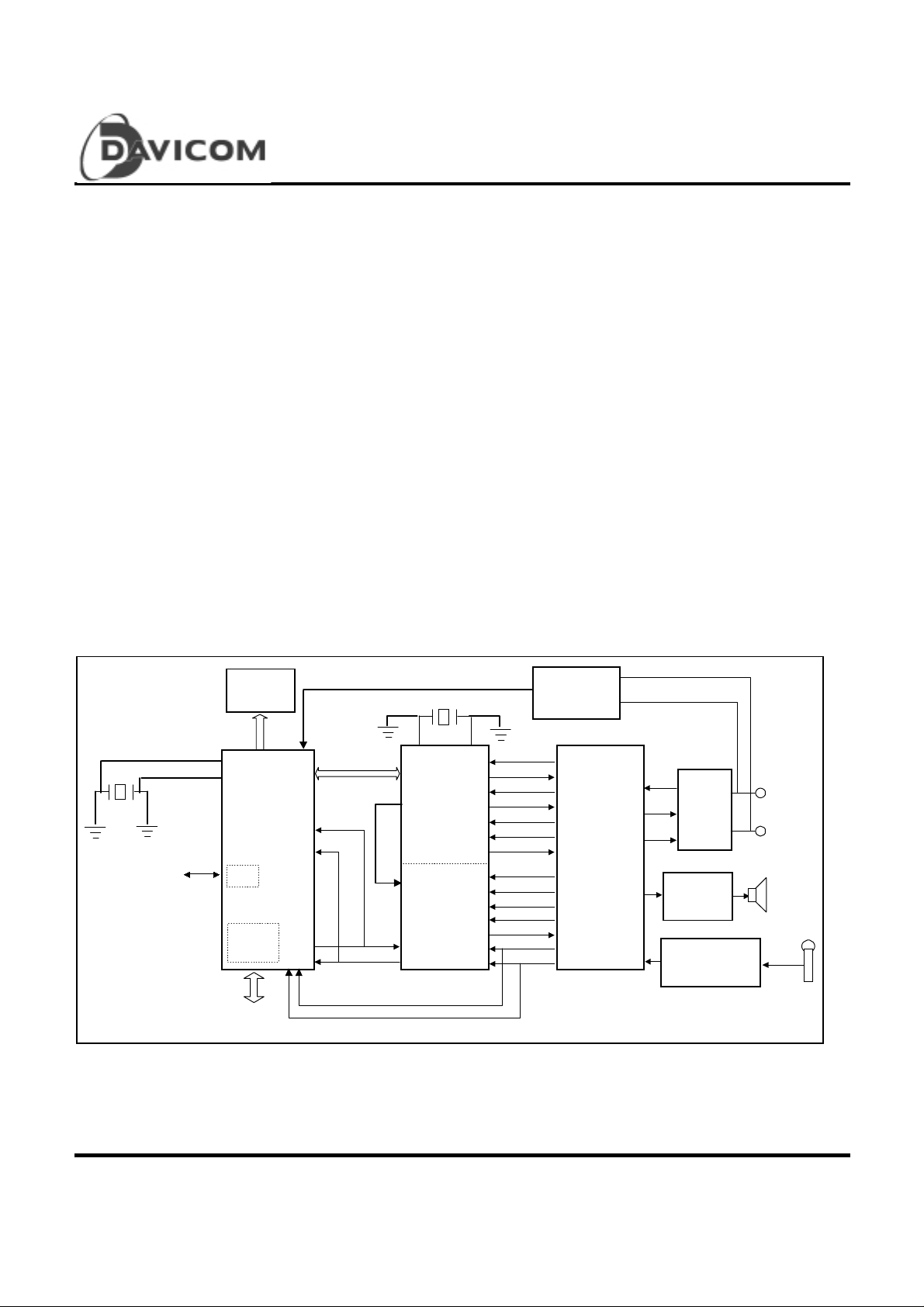
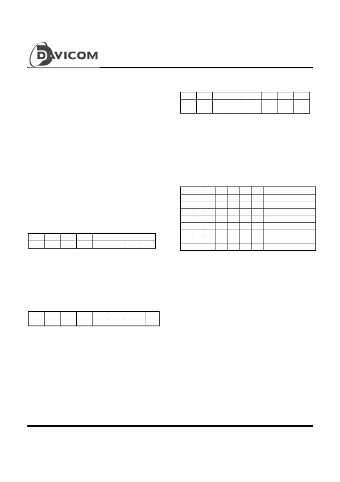
Block Diagram
The DM560P modem reference design is preapproved for FCC part 68 and provides minimum
design cycle time, with minimum cost to insure the
maximum amount of success.
The simplified modem system, show n in figure
below, illustrates the basic interconnection between
the MCU, DSP, AFE and other basic co m ponents of
a modem. The individual elements of the DM560P
are:
• DM6580 Analog Front End (AFE). 28-pin PLCC
package
• DM6581 ITU-T V.90 Transmit Digital Signal
Processor (TX DSP). 100-pin QFP package
• DM6582 ITU-T V.90 Receive Digital Signal
Processor (RX DSP). 100-pin QFP package
• DM6583 Modem Controller (MCU) built in Plug &
Play (PnP). 100-pin QFP package
29.4912
MHz
ISA Bus
LED
DM658
3
Micro
Controller
Unit
PnP
V.24
Interface
V.24
Interface
Address &
Data Bus
MSCLK
TxD
RxD
40.32MHz
DM658
1
TX DSP
DM658
2
RX DSP
Detector
SCLK
DIT
DOT
TFS
DIR
DOR
RFS
TxBCLK
TxSCLK*2
RxBCLK
RxSCLK
20.16MHz
TxDCLK
RxDCLK
Ring
DM658
0
Analog
Front End
SPKR
RxIN
TxA1
DAA
TxA2
Speaker
Driver
Microphone
Driver
Lin
e
Preliminary 1
Version: DM560P -DS-P07
August 11, 2000

DM560P
V.90 Integrated Data/Fax/Voice/Speakerphone Modem Device Set
Table of Conten ts
General Descri pti on 1
Block Diagram 1
Features 3
Chipset
Chip 1: DM6583 Modem Controller Unit with PnP
DM6583 Description 4
DM6583 Block Diagram 4
DM6583 Features 4
DM6583 Pin Configuration 5
DM6583 Pin Description 6
DM6583 Functional Description 8
1. Operating Mode Selection 8
2. Micro-controller (8032) Reference 8
3. Micro-c ontroller Register Description 8
4. UART (16550A) Emulation Registers 9
5. Plug and Play (PnP) Module 16
DM6583 Absolute Maximum Ratings 24
DM6583 Electrical Characteristics 24
DM6583 Timing Diagrams 25
Chip 2: DM6581 ITU-T V.90 TX DSP
Chip 3: DM6582 ITU-T V.90 RX DSP
DM6581/82 Description 26
DM6581/82 Block Diagram 26
DM6581/82 Features 26
DM6581/82 Pin Configuration 27
DM6581/82 Pin Description 28
DM6581/82 Functional Description 29
1. System Cloc k 29
2. Serial Port 29
3. Dual Port RAM 30
4. Interrupt 30
DM6581/82 Absolute Maximum Ratings 31
DM6581/82 Electrical Characteristics 31
DM6581/82 Timing Diagrams 32
Chip 3: DM6580 Analog Front End
DM6580 Description 33
DM6580 Block Diagram 33
DM6580 Features 34
DM6580 Pin Configuration 34
DM6580 Pin Description 35
DM6580 Functional Description 35
DM6580 Absolute Maximum Ratings 37
DM6580 DC Characteristics 37
DM6580 AC Characteristics & Timing Diagrams 37
DM6580 Performance 37
Package Information 38
Ordering Information 40
Company Overview 40
Contacts 40
Appendix A-1 Internal Card Application Circuit 41
Appendix A-2 Internal Card Reference B.O.M. 42
Appendix B Copy Of FCC Approval Certificate 43
2 Preliminary
Version: DM560P -DS-P07
August 11, 2000

Features
DM560P
V.90 Integrated Data/Fax/Voice/Speakerphone Modem Device Set
Set
■ Compatibility
- ITU-T V.90 (56000 to 28000 bps)
- ITU-T V.34 (33600 to 2400 bps)
- CCITT V.32bis (14400, 12000, 9600, 7200,
4800bps)
- CCITT V.32 (9600, 7200, 4800bps)
- CCITT V.22bis (2400, 1200bps)
- CCITT V.22 (1200bps)
- CCITT V.23 (1200/75bps)
- Bell 212A (1200bps)
- Bell 103 (300bps)
■ Fax
- CCITT V.17 (14400, 12000, 7200bps)
- CCITT V.29 (9600, 7200bps)
- CCITT V.27ter (4800, 2400bps)
- CCITT V.21 Channel 2 (300bps)
- Group III, Class 1
■■■■ Data Error Correction
- MNP Class 4
- CCITT V.42 LAPM
■ Data Compression
- MNP Class5
- CCITT V.42bis
■ Voice compression
- 2 and 4 bit ADPCM
- IMA ADPCM (Developing)
- 8 Bit PCM
■ DTE Interface
- DTE speed up to 115200bps
■ Enhanced T” command set and S registers
- TIA/EIA 578 Fax Class 1 command set
- TIA/EIA IS-101 Voice command set
■ Video-ready modem interface V.80(Developing)
■ V.8bis (Developing)
■ Integrated UART 16550
■ Parallel and Serial interfaces
- 6, 7 and 8 bit character support
- Even, odd, mark and none parity detection and
generation
- 1 and 2 stop bit support
- Auto DTE data speed detection through “AT”
■ Caller identification (Caller ID) support
■ Speakerphone
■ Selectable world wide call progress tone detection
■ 16 Bit over-sampling codec
■ Compromise and adaptive equalizer providing
channel impairment compensation
■ Plug and Play (PnP) support
■ Enhanced 8032 compatible mi cro-c o ntroll e r
■ Power Management (power down mode)
■ 8 selectable interrupts
■ Access up to 256K bytes external program
memory
■ Access up to 64K bytes external data memory
■ NVRAM to store two user configurable, selectable
profiles with three programmable telephone
numbers
■ Full duplex data mode test capabilities
- Analog loop test
- TIA/EIA 602, ITU V.25 ter AT command
Chipset
The DM560P integrated modem device set contains 4 VLSI devices as described below:
1. DM6583 Modem Controller Unit with PnP for ISA
2. DM6580 Analog Front End (AFE)
3. DM6581 ITU-T V.90 Transmit Digital Signal Processor (TX DSP)
4. DM6582 ITU-T V.90 Receive Digital Signal Processor (RX DSP)
Preliminary 3
Version: DM560P -DS-P07
August 11, 2000
V.90 Integrated Data/Fax/Voice/Speakerphone Modem Device Set
Chip 1: Modem Controller Unit with Pn P for ISA
DM6583 Description
The DM6583 Modem Control Unit is designed for
use in high speed internal and external modem
applicati ons. The DM6583 interface is compatible
with the DM6581/DM6582 Transmit and Receive
Digital Signal Processors. The DM6583 incorporates
a 80C32 micro-controller, a virtual 16550A UART
with FIFO mode, and Plug & Play control logic.
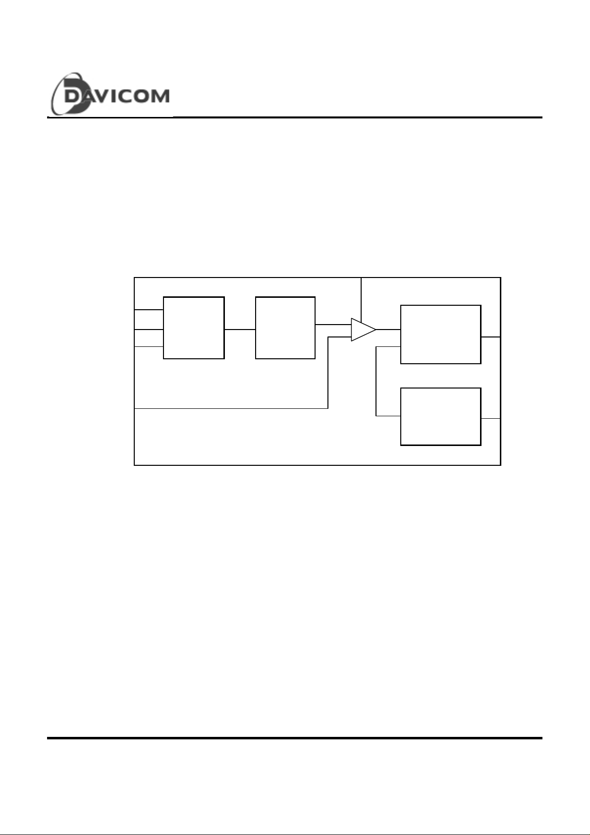
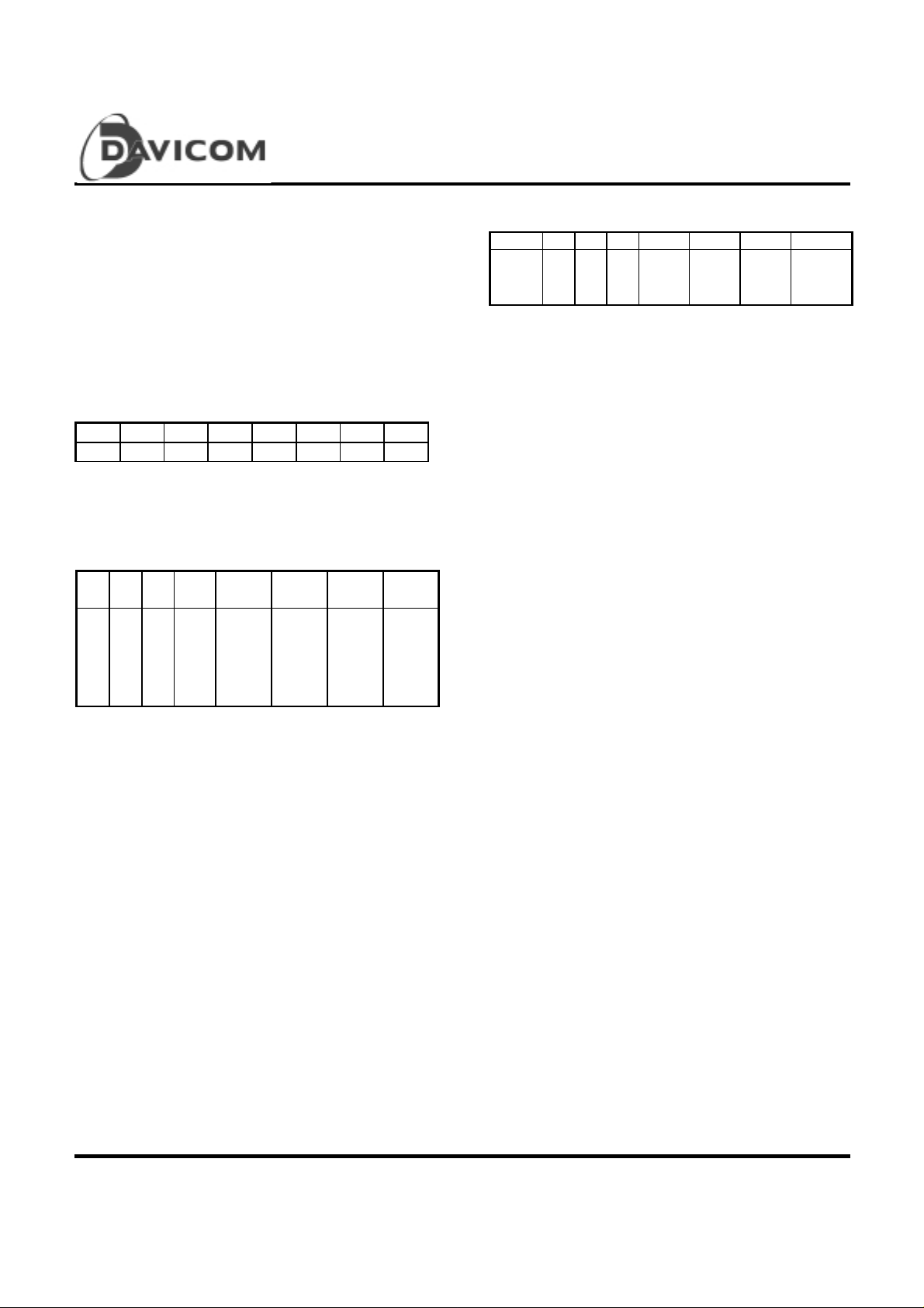
DM6583 Block Diagram
PC Data Bus
PC Address Bus
IRQ & R/W Control
PnP Control
Logic
Virtual 16550
UART
DM560P
The DM6583 MCU performs general modem control
functions, and is also designed to provide Plug and
Play capability for ISA bus systems. The Plug and
Play logic supports software or automatic Plug and
Play selectable I/Os to allow users to configure the
internal modem card without jumpers.
Mode Selection
8032
Micro-Controller
External ROM,
RAM Interface
RS 232 Interface
DM6583 Features
• Control interface support
• Supports parallel and serial interfaces
• Includes a 80C32 micro-controller
• 256K bytes maximum external program memory
• 64K bytes maximum external data memory
• Provides automatic Plug and Play or software
configuration capabilities
• 8 selectable Interrupts
I/O Control Logic
• Conflict free I/O base address selection
• Virtual 16550A UART compatible parallel
interface
• Fully programmable serial interface:
- 6, 7 or 8-bit characters
- Even, odd, mark and none parity bit generation
and detection
- 1 and 2 stop bit generation
- Baud rate generation
- Includes I/O control logic for modem control
interface
Modem Control
Interface
4 Preliminary
Version: DM560P -DS-P07
August 11, 2000
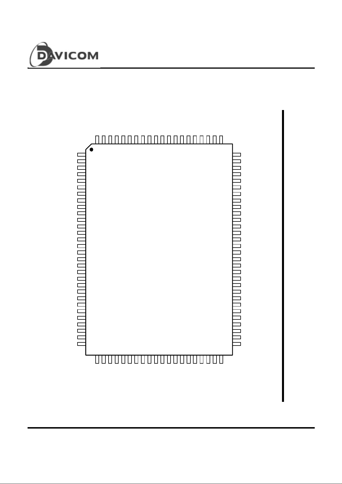
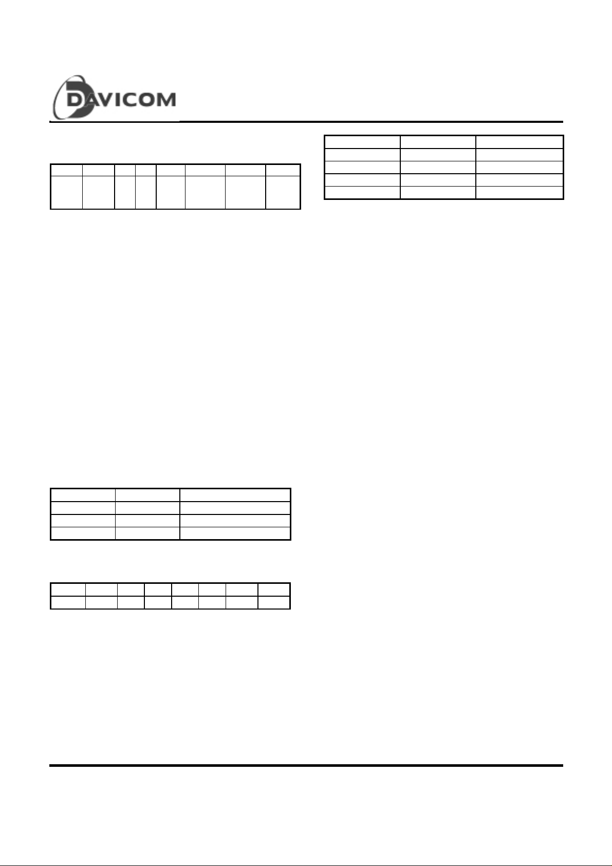
DM6583 Pin Configuration
DM560P
V.90 Integrated Data/Fax/Voice/Speakerphone Modem Device Set
UD0
UD1
UD2
UD3
UD4
UD5
UD6
UD7
/IOR
GND
/IOW
/AEN
A11
A10
A9
A8
A7
A6
A5
A4
A3
A2
A1
A0
V
DD
IRQ4
IRQ5
IRQ7
IRQ10
RESET
1
2
3
4
5
6
7
8
9
10
11
12
13
14
15
16
17
18
19
20
21
22
23
24
25
26
27
28
29
30
DD
EXT/INTB
V
99
100
32
31
PS1
98
33
GND
/TUCS
96
97
35
34
A12
A13
A14
A15
/PNPEN
91
92
93
94
95
DM6583
39
38
37
36
voice sel2
/POR
Voice Sel1
88
89
90
43
424041
TXRCLK
RXRCLK
86
87
45
44
GND
85
46
D0
84
47
D1
83
48
D2
82
49
D3
81
50
80
79
78
77
76
75
74
73
72
71
70
69
68
67
66
65
64
63
62
61
60
59
58
57
56
55
54
53
52
51
D4
D5
D6
D7
CA0
CA1
CA2
CA3
CA4
CA5
CA6
CA7
GND
CA8
CA9
CA10
CA11
CA12
CA13
CA14
CA15
IRQ3
/RD
/WR
/PSEN
ALE/P
TXD
RXD
V
DD
/LCS
XTAL2
XTAL1
IRQ12
IRQ11
DD
V
IRQ15
/PWR
CA17
CA16
/RUCS
GND
T0
T1
/RI
/DTR
/OH
/VOICE
EEPROM1
EEROM3
EEPROM2
Preliminary 5
Version: DM560P -DS-P07
August 11, 2000

V.90 Integrated Data/Fax/Voice/Speakerphone Modem Device Set
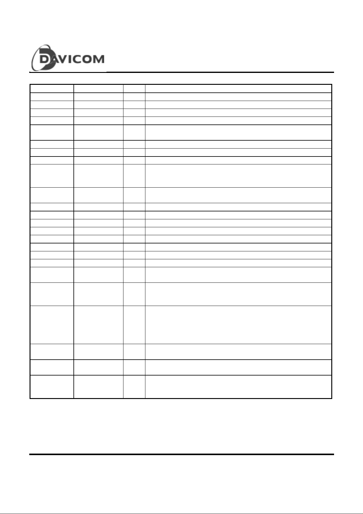
DM6583 Pin Description
Pin No. Pin Name I/O Description
1 - 8 UD0 - UD7 I/O Data Bus Signal, for internal modem:
These signals are connected to the data bus of the PC I/O. They are
used to transfer data between the PC and the DM6583.
Modem Control Output, for external modem:
Memory address mapping of the contr oller is E800H.
9 /IOR I I/O Rea d:
An act ive lo w input signal used to read data from the DM6583.
10, 41, 68,
85, 96
11 /IOW I I/O Writ e :
12 /AEN I Address Enable:
13 - 24 A11 - A0 I System Address:
25, 36, 52,
100
26, 27, 28,
29, 33, 34,
35, 59
30 RESET I Reset:
31 XTAL1 I Cryst al Oscillator Input
32 XTAL2 O Crystal Oscillator Output
37 /PWR O Controller P rogram Write Enable:
51 /LCS I Loop Current Detection. Modem Input Control:
39 /RUCS O RX DSP Register Select Output:
40,38 CA16,CA17 O Bank Switch Control:
42 T0 I Controller Counter 0 Input
GND P Ground
An act ive lo w input signal used to write data to the DM6583.
This is an active low signal to enable the system address for
DM6583.
These signals are connected to the bus of PC I/O. They are used to
select DM6583 I/O ports.
A0~A7:Modem Control Input for external modem. Memory address
mapping of the controller is E800H.
VDD P +5V Power Supply
IRQ4, IRQ5,
IRQ7, IRQ10,
IRQ11, IRQ12,
IRQ15, IRQ3
O Interrupt Request:
These are the interrupt request pins. Only one pin, which is
decoded from Configuration Register can be active. The active pin
will go high when an interrupt request is generated from the
DM6583.
An active high signal used to reset the DM6583.
This pin is used to enable FLASH ROM programming. In
conf igurations with no FLASH memory, this pin is not connected.
This pin is mapped to bit0 of address D000H.
Memory address mapping of the contr oller is E400H.
These signals are used to switch external program memory
between banks.
CA16 CA17
Bank 0 0 0
Bank 1 1 0
Bank 2 0 1
Bank 3 1 1
DM560P
6 Preliminary
Version: DM560P -DS-P07
August 11, 2000
DM560P
V.90 Integrated Data/Fax/Voice/Speakerphone Modem Device Set
DM6583 Pin Description
Pin No. Pin Name I/O Description
43 T1 I Controller Counter 1 Input
44 /RI I Ring Signal Input
45 /DTR I DTR Input Pin (P1.1)
46 /OH O Hook Relay Control (P1.2)
47 /VOICE O Voice Relay Control. Modem Control Output (memory map is bit
48-50 EEPROM 1-3 I/O EEPROM Control Pins (P1.4-P1.6)
53 RXD I Controller Serial Port Data Input
54 TXD O Controller Serial P ort Data Output
55 ALE/P O Controller Address Latch Enable:
56 /PSEN O Controller Program Store Ena ble:
57 /WR O Controller External Data Memory Write Contro l
58 /RD O Controller External Dat a Memory Read Control
60 - 67 CA15 - CA8 O Controller Address Bus
69 - 76 CA7 - CA0 O Controller Address Bus
77 - 84 D7 - D0 I/O Controller Data Bus
86 TXRCLK I Transmitter Baud Rate Clock Input (Controller INT 0)
87 RXRCLK I Receiver Baud Rate Clock Input (Controll er INT 1)
88 /POR O DSP Reset Output
89, 90 VOICE Se1 1
VOICE Se1 2
91 - 94 A12 - A15 I System Address:
95 /PNPEN I PnP Mode Enable:
97 /TUCS O TX DSP Register Select Output:
98 PS1 O Modem Control Port Select Output:
99 EXT/INTB I Select Pin: Used to select internal or external operation.
(continued)
3 of DAA)
Output pulse for latching the low byte of the address during
accesses to the extern al memory.
This output goes low during a fetch from external program memory.
O Modem C o ntro l Out put (Memory map is bit 1-2 of DAA at memory
address D000H)
These signals are connected to the bus of the PC I/O. They are
used to select the DM6583 I/O ports.
This pin selects PnP mode. When connected to ground, the
DM6583 will enter PnP mode when it receives the PnP initiation key
sequence. When disconnected, an internal pull up will disable the
Plug and Play function.
Memory address mapping of the contr oller is F000H.
Memory address mapping of the contr oller is D800H.
0: internal modem
1: external modem
Preliminary 7
Version: DM560P -DS-P07
August 11, 2000

DM560P
V.90 Integrated Data/Fax/Voice/Speakerphone Modem Device Set
DM6583 Functional Description
1. Operating Mode Selection
The DM6583 MCU can be used in both internal and
external modem applications. When operating as an
internal modem, the EXT/INTB input (pin 99) must
be attached to ground. When the DM6583 is
operating as an external modem, the EXT/INTB
input (pin 99) must attached to VDD.
2. Micro-controller Program Memory
The DM6583 supports two bank switch control pins
to switch external program memory among four
banks. The DM6583 can access a total of 256K of
external pr ogram mem ory.
Address mappi ng:
bank0: 00000H - 0FFFFH
bank1: 10000H - 1FFFFH
bank2: 20000H - 2FFFFH
bank3: 30000H - 3FFFFH
For bank switching, three instruc tions must be
included in software.
Switch to bank1:
CLR P1.3
SETB P1.7
JMP BANK 1 ADDRESS
Switch to bank2:
CLR P1.7
SETB P1.3
JMP BANK 2 ADDRESS
Micro-contro ller Power Down Mode
An instruction that sets the register PD (PCON.1) will
cause the 80C32 to enter power down mode. There
are three ways to wake up the 80C32
(1) Positive pulse signal occurring at the reset pin of
the 80C32
(2) Negative pulse occurring at / R I (P1.0) of the
80C32
(3) Programming the PnP Wake Up Controller
Register.
Enhanced Internal direct Memory
There are two 128 byte banks of intern al direc t
memory in the 80C32. The system uses the lower
128 bytes under normal conditions. Switching to the
upper bank is achieved by loading register 8FH.1
(SFR of the 80C32) with 1. Switching to the lower
bank can be achieved by loading the same register
with 0.
Reflash Program Memory
By setting 8F.2H the system can switch program and
data memory. If the system uses FLASH memory as
program memory this function is used to reflash
program code by downloading the program to data
memory then switching them.
Example:
SETB 8FH.2
LJMP 0000H
Switch to bank3:
CLR P1.7
CLR P1.3
JMP BANK 3 ADDRESS
Return to bank 0:
SETB P1.7
SETB P1.3
JMP BANK 0 ADDRESS
* For detailed information about the micro-controller,
refer to the Programm er's Guid e to 8032.
8 Preliminary
Micro-controller Register Description
UART Clock Register:
Address D4000H Reset State: 06H
Write Only
bit7 bit6 bit5 bit4 bit3 bit2 Bit1 bit0
X dat6 dat5 dat4 dat3 dat2 dat1 0
Version: DM560P -DS-P07
August 11, 2000
DM560P
V.90 Integrated Data/Fax/Voice/Speakerphone Modem Device Set
UART Clock
The internal clock of the virtual UART logic is fixed at
1.8432MHz. The clock is derived from the MSCLK
signal from the DM6582 DSP, or an external 30Mhz
crystal. The UART 1.8432MHz clock will be obtained
by division. When the operating frequency of the
DM6583 controller changes, the divider should be
changed accordingly. This divider is specif ie d by the
Configuration Register which can be written by the
DM6583 controller. The address mapping of the
register is D400H: ( DM 6583 controller memory
mapping)
Bit 0: Always 0.
Bit 6-1 : define the cloc k divider range from 2 to 64
(even number).
Bit 7: Not used.
UART Baud Generator Divisor Latch Register:
Address EC00H
Read only
bit7 bit6 bit5 bit4 bit3 bit2 bit1 bit0
dat7 dat6 dat5 dat4 dat3 dat2 dat1 dat0
Modem Output Port Regi st er: Address D000H
Write only
bit7 bit6 bit5 bit4 bit3 bit2 bit1 bit0
/Voice Voice
These 4 bits control the DM6583 output ports.
PnP Isolation & Resource Data Port: Address
F800H
Write only
The PnP isolation and resource data can be bytesequentially written to the corresponding memory
through this register.
Auto-configuration Register: Address F400H
bit2 bit1 bit0 IRQ bit5 bit4 bit3 I/O
0 0 0 3 0 0 0 03F8-03FF(COM1)
0 0 1 4 0 0 1 02F8-02FF(COM2)
0 1 0 5 0 1 0 03E8-03EF(COM3)
0 1 1 7 0 1 1 02E8-02EF(COM4)
1 0 0 10 1 0 0 03F0-03F7(COM5)
1 0 1 11 1 0 1 02F0-02F7(COM6)
1 1 0 12 1 1 0 03E0-03E7(COM7)
1 1 1 15 1 1 1 02E0-02E7(COM8)
-sel2
Voice
-Sel1
/POR
By reading this register, the micro-controller can
monitor the value of the low byte divisor latch of the
virtual UART baud generator (see DLL in next
section) and determine the baud rate clock itself.
Modem Status Control Register (MSCR):
Address E000H
Write only
bit7 bit6 bit5 bit4 bit3 bit2 bit1 bit0
0000/CTS/DSR/DCD/RI
This register contains information about the line
status of the modem. The available signals are Ring
Detect (/RI), Carrier Detect (/DCD) , Data Set Ready
(/DSR) and Clear To Send (/CTS).
The default I/O base and IRQ data stored in 93C46 is
loaded to this register by the micro-controller. The
micro-controller can also get the current I/O base
and IRQ information settings by performing a read
from this register. The configuration determined by
this register will be disabled when the register
detects the Initiation Key described in the next
section.
Bit 6: This bit is set to inform micro-controller that the
current I/O base and IRQ data should be stored to
93C46 as the default setting for the next power-on
reset through programming the Auto-configuration
Register. This bit will be cleared by micro-controller.
Bit 7: When bit 7 is set, it enables the hardware
configuration to be set according to bit 0-bit 5
(Jumperless mode) and loads the proper value into
the PnP Registers including I/O and Interrupt
Configuration Registers. This bit will be reset, when it
receives PnP Initiation Key sequence.
Preliminary 9
Version: DM560P -DS-P07
August 11, 2000

V.90 Integrated Data/Fax/Voice/Speakerphone Modem Device Set
Auto-configuration Register: Address F400H
(continued)
* When a reset condition occurs, the I/O and
Interrupt configuration registers must be reset to the
default value according to bit 0 - bit 5.
RxDataBits Register: Address DC00H
Write only
Once the RxDataBit set to 1, the data in the RxBuffer
will be transferred to RxFiFo. The transfer bit number
is the same as the programming valu e of RxDataBits
Register.
RxBuffer: Address DC01H
Write only
Receive data will be written to the RxBuffer and will
be input to the RxHDLC circuit. The RxBuffer is 16
bytes wide.
RxFiFo: Address DC01H
Read only
After the data has been passed from the RxBuffer to
the RxHDLC circuit, the RxHDLC circuit will remove
the 7eH patterns and transfer the results to the
RxFiFo. There RxFiFo is 21 bytes wide.
TxDataBits Register: Address DC02H
Write only
Data written to TxDataBits will be presented to the
TxFiFo. The data in TxFiFo will be transferred to
TXHDLC circuit. The transfer bit number is the same
as the value of TxDataBit s register. If the TxFiFo is
empty, a 7e pattern will be loaded to the TxFiFo. If
TxFiFo is not empt y and the data frame has the
pattern of five consecutive “1” , then the TXHDLC
circuit will insert “0” automatically.
TxFiFo Register: Address DC03H
Write only
The o riginal HDLC frame data will be loaded to the
TxFiFo, presented to the input of the TxHDLC circuit.
The TxFiFo is 21 bytes wide.
TxBuffer: Address DC03H
Read only
According to TxDataBits, the TxHDLC circuit will
transfer the same number data bits to the TxBuffer.
The TxBuffer i s 16 bytes wide.
DM560P
HDLC CNTL/STATUS Register: Address DC04H
Bit0: TxReady0
0: indicates the data in the TxFiFo has deceased
to zero and the HDLC circuit has transferred
st
7eH pattern.
the 1
1: indicates that the TxFiFo data is greater than or
equal to the threshold value.
Bit1: Rxdata
0: all the data in the RxBuffer has been read.
1: Programed by software to indicate that all data
in the RxDataBits register has been written to
the RxBuffer.
Bit2: TxF i Fo Thr e shold
0: TxFiFo threshold No. = 11
1: TxFiFo threshold No. = 16
Bit3: TxFiFo Status
0: data No. in TxFiFo >= threshold
1: data No. in TxFiFo <= threshold
Bit4: Txda ta
0: A write action to TxDataBites register will clear
this bit.
1: Bit No. in TxBuffer = TxDataBits register.
Bit5: RxFiFo empty
0: data bytes No. in RxFiFo <>0
1: data bytes No. in RxFiFo = 0
Bit6: Reset
0: Normal state
1: reset HDLC circuit
In____ buffer register: Address DC08
writ e only
Controller write the original data to this temp buffer.
Out ____ buffer register: Address DC08H
read only
Controller read the result data from this buffer
Status/Rst register: Address DC09H
Bit0: data ready f lag (read only)
1: data has been load to out _ buffer. (clear
automatically by a read from out_ buffer)
0: data hasn’t been load to out _ buffer.
Bit1: frame end flag (read only)
1: Indicate end of HDLC frame (clear by a reset
action)
Bit2: fram ready flag (read only)
1: CRC check ok.
0: CRC check fail.
Bit3: In _ buffer empty flag
10 Preliminary
Version: DM560P -DS-P07
August 11, 2000
V.90 Integrated Data/Fax/Voice/Speakerphone Modem Device Set
1: In _ buffer empty (clear automatically by a
write to In _buffer)
0: In _ buffer not empty
Bit7: reset bit(write only)
1: software reset
(4)CRCL register: Address DC0AH (read only)
(5)CRCH register: Address DC0BH (read only)
UART (16550A) Emulation Regist ers
Receiver Buffer (Read), Transmitter Holding
Register (Write): Address: 0 (DLAB=0)
Reset State 00h
bit7 bit6 bit5 bit4 bit3 Bit2 bit1 bit0
dat7 dat6 dat5 dat4 dat3 Dat2 dat1 dat0
When this register address is read, it contai ns the
parallel received data. Data to be transmitted is
written to this registe r .
Interrupt Enable Register (IER): Address 1
DM560P
Interrupt Identification Register (IIR): Address 2
Reset State 01h, Read only
Bit7 Bit6 bit5 bit4 bit3 bit2 bit1 bit0
FIFO
Enable
In order to provide minimum software overhead
during data transfers, the virtual UART prioritizes
interrupt s into four levels as follows: Receiver Line
Status (priority 1), Receiver Data Available (priority
2), Character Timeout Indi cation (priority 2, FIFO
mode only), Transmitter Holding Register Empty
(priorit y 3), and Modem Status (priority 4).
The IIR register gives pri ori tized information
regarding the status of i nterrupt conditions. W hen
accessed, the IIR indic ates the highest priority
interrupt that is pending.
000D3:
INTD2
D2:
INTD1
D1:
INTD0
D0:
int
Pending
Reset State 00h, Write Only
bit7 bit6 bit5Bit4 bit3 bit2 bit1 bit0
0 0 0 0 Enable
Modem
Status
Intr
Enable
Line
Status
Intr
Enable
TX
Holding
Registe
r
Intr
Enable
RX
Data
Intr
This 8-bit register enables the four types of interrupts
as described below. Each interrupt source can
activate the INT output signal if enabled by this
register. Resetting bits 0 through 3 will disable all
UART interrupts.
Bit 0: This bit enables the Received Data Avail able
and timeout interrupts in the FIFO mode when
set to logic 1.
Bit 1: This bit enables the Transmitter Holding
Register Empty Interrupt when set to logic 1.
Bit 2: This bit enables the Receiver Line Status
Interrupt when set to logic 1.
Bit 3: T his bit enables the MODEM Status Interrupt
when set to logic 1.
Bit 0: Thi s bit c an be used in either a prioritized
interrupt or polled environment to indicate
whether an interrupt is pending. When this bit
is a logic 0, an interrupt is pending, and the IIR
contents may be used as a pointer to the
appropriate interrupt service routine. When bit
0 is a logic 1, no int er r upt is pending, and
polling (if used) continues.
Bit 1-2: The se tw o bit s of the IIR are used to identify
the highest priority interrupt pending, as
indicated in the table below.
Bit 3: In character mode, this bit is 0. In FIFO mode,
this bit is set, along with bit 2, when a timeout
interrupt is pending.
Bit 4-6: Not used
Bit 7: FIFO always enabled.
Bit 4-7: Not used
Preliminary 11
Version: DM560P -DS-P07
August 11, 2000

DM560P
V.90 Integrated Data/Fax/Voice/Speakerphone Modem Device Set
Interrupt Identification Register (IIR): Address 2 (continued)
D3 D2 D1 D0 Priority Level Interrupt Type Condition Reset
0001- - - 0 1 1 0 Highest Receiver Line
Status
0 1 0 0 Second Receiver Data
Available
1 1 0 0 Second Character Timeout
Indication
0 0 1 0 Third Transmitter
Holding Register
Empty
0 0 0 0 Fourt h Modem Status Cl ear to Send, Data Set
Overrun Error, Pari ty E rro r,
Framing Error or Break
Interrupt
Receiver Data Available or
Trigger Lev el Reached
No characters have been
read from or written to the
Rx FIFO during
programming time interval,
and the Rx FIFO is not
empty
Ready to accept new data
for transmi ssion
Ready, Ring Indi c ator or
Data Carrier Detected
Reads the Line Status
Register
Reads the Receiver Buff er
Register or the F IFO has
Dropped Below the
threshold value
Reads The Receiver Buff er
Register
Reads the IIR Register or (if
source of interrupt) W rites
To The Transmitter Holding
Register
Reads the Modem Status
Register
12 Preliminary
Version: DM560P -DS-P07
August 11, 2000
DM560P
V.90 Integrated Data/Fax/Voice/Speakerphone Modem Device Set
FIFO Control Register (FCR): Address 2
Reset State 00h , write only
bit7 bit6 bit5 bit4 bit3 bit2 bit1 bit0
RCVR
(MSB)
Trig
RCVR
Trig
(LSB)
00DMA
Mode
TxFIFO
Reset
RxFIFO
Reset
FIFO
Enable
This is a write only register at the same location as
the IIR, which is a read only register. This register is
used to enable the FIFOs, clear the FIFOs, set the
RxFIFO trigger level, and select the type of DMA
signal.
Bit 0: FIFO Enable, This bit is always high
Bit 1: Writing a 1 to FCR1 clears all bytes in the
RxFIFO and resets the counter logic to 0.
Bit 2: Writing a 1 to FCR2 clears all bytes in the
TxFIFO and resets the counter l ogic t o 0.
Bit 3: Setting FCR3 to 1 will cause the RXRDY and
TXRDY pins to change from mode 0 to mode 1
if FCR0 = 1.
Bit 4-5: Reserved
Bit 6-7: FCR6, FCR7 are used to set the trigger level
for the RxFIFO i nterrupt.
WLS1 WLS0 Word Length
005 bits
016 bits
107 bits
118 bits
Bit 0-1: WLS0-1 specifies the number of bits in each
transmitted and received serial character.
Bit 2: STB specifies the numbe r of sto p bits in each
transmitted character. If bit 2 is a logic 0, one
sto p bit is generated in the transmitted data. If
bit 2 is a logic 1 when a 5-bit word length is
selected via bits 0 and 1, one and a half stops
are generated. If bit 2 is a logic 1 when either a
6-, 7- or 8-bit word length is selected, two stop
bits are generated. The Receiver checks the
first Stop-bit only, regardless of the number of
Stop bits selected.
Bit 3: Logic 1 indicates that the PC has enabled
parity generation and checking.
Bit 4: Logic 1 indicates that the PC is requesting an
even number of logic 1s (even parity
generation) to be transmitted or checked.
Logic 0 indicates that the PC is requesting odd
parity generation and checking.
FCR6 FCR7 RxFIFO Trigger Level
00 01
01 04
10 08
Line Control Register (LCR): Address 3
Reset State 00h, Write Only
bit7 bit6 bit5 bit4 bit3 bit2 bit1 bit0
DLAB SBRK STP EPS PEN STB WLS1 WLS0
This register is available to maintain compatibility
with the standard 16550 register set, and provides
information to the internal hardware that is used to
determine the number of bits per character.
Preliminary 13
Version: DM560P -DS-P07
August 11, 2000
Bit 5: When bits 3, 4 and 5 are logic 1, the parity bit
is transmitted and checked by the receiver as
logic 0. If bits 3 and 5 are 1 and bit 4 is lo g ic 0,
then the parity is transmitted and checked as
logic 1.
Bit 6: This is a Break Control bit. When it is set to
logic 1, a break condition is indicated.
Bit 7: The Divisor Latch Access bit must be set to
logic 1 to access the Divisor Latches of the
baud generator during a read or write
operation. It must be set to logic 0 to access
the Receiver Buffer, the Transmitter Holding
Register, or t he Interrupt Enable Register.
 Loading...