


Davicom DM6383F, DM6382F, DM6381F, DM6380L Datasheet
General Description
DM336P
V.34 Integrated Data/ Fax/Voice/Speakerphone Modem Device Set
The DM336P integrated modem is a four chipset
design that provides a complete solution for state-ofthe-art, voice-band Plain Old Telephone Service
(POTS) communication. The modem provides for
Data (up to 33,600bps), Fax (up to 14,400bps), Voice
and Full Duplex Speaker-phone functions to comply
with various international standards.
The design of the DM336P is optimized for desktop
personal com puter applications and it provides a low
cost, highly reliable, maximum integration, with the
minimum am ount of support required. The DM336P
modem can operate over a dial-up network (PSTN) or
2 wire leased lines.
The modem integrates auto dial and answer
capabilities, synchronous and asynchronous data
transmi ssions, seri al and parallel interfaces, various
tone detection schemes and data test modes.
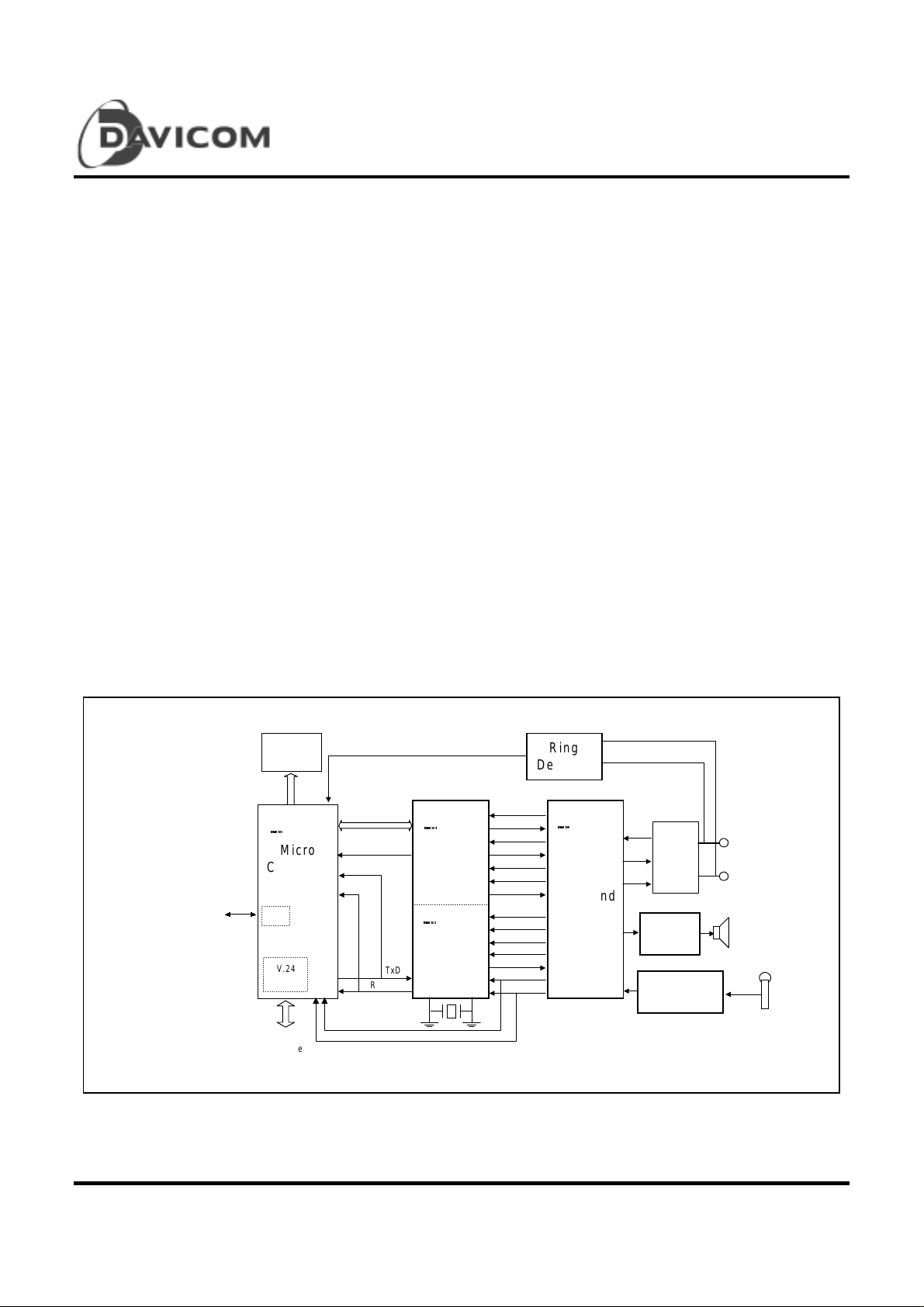
Block Diagram
The DM336P modem’s reference design is preapproved for FCC part 68 and provides minimum
design cycle time, with minimum cost to insure the
maximum amount of success.
The simplified modem system, shown in figure below,
illustrates the basic interconnection between the
MCU, DSP, AFE and other basic components of a
modem. The individual elements of the DM336P are:
• DM6380 Analog Front End (AFE). 28-pin PLCC
package
• DM6381 ITU-T V.34 Transmit Digital Signal
Processor (TX DSP). 100-pin QFP package
• DM6382 ITU-T V.34 Receive Digital Signal
Processor (RX DSP). 100-pin QFP package
• DM6383 Modem Controller (MCU) built i n Plug &
Play (PnP). 100-pin QFP package
SCLK
DIT
DOT
TFS
DIR
DOR
RFS
RxDCLK
Ring
Detector
Analog
Font End
SPKR
RxIN
TxA1
DAA
TxA2
Speaker
Driver
Microphone
Driver
Line
LED
Address &
Micro
Data Bus
MSCLK
TX DSP
Controller
Unit
ISA Bus
PnP
RX DSP
V.24
Interface
V.24
Interface
Final 1
Version: DM336P- DS-F02
August 15, 2000
TxD
RxD
40.32MHz
TxBCLK
TxSCLK*2
RxBCLK
RxSCLK
20.16MHz
TxDCLK

V.34 Integrated Data/ Fax/Voice/Speakerphone Modem Device Set
Table of Conten ts
General Descri pti on ............................................... 1
Block Diagram ....................................................... 1
Features................................................................3
Chipset
• Chip 1: DM6383 Modem Controller Unit with PnP
for ISA (MCU)
DM6383 Description ........................................... 4
DM6383 Block Diagram...................................... 4
DM6383 Features............................................... 4
DM6383 Pin Configuration.................................. 5
DM6383 Pin Description ..................................... 6
DM6383 Functional Description .......................... 8
1. Operating Mode Selection............................ 8
2. Micro-controller (8031) Reference................ 8
3. Micro-controller Register Description............ 8
4. UART (16550A) Emulation Registers ........... 9
5. Plug and Play (PnP) Module .......................14
DM6383 Absolute Maximum Ratings .................20
DM6383 DC Electrical Characteristics................21
DM6383 AC Electrical Characteristics & Timing
Waveforms.....................................................21
DM336P
DM6381/82 Functional Description....................26
1. System Clock.............................................26
2. Serial Port ..................................................26
3. Dual Port RAM...........................................26
4. Interrupt......................................................26
DM6381/82 Absolute Maximum Ratings ............26
DM6381/82 DC Electrical Characteristics...........27
DM6381/82 AC Electrical Char ac teristics & Timing
Waveforms.....................................................27
• Chip 3: DM6380 Analog Front End (AFE)
Description
DM6380 Description..........................................29
DM6380 Block Diagram..................................... 29
DM6380 Features..............................................30
DM6380 Pin Configuration.................................30
DM6380 Pin Description....................................31
DM6380 Functional Description.........................31
DM6380 Absolute Maximum Ratings .................32
DM6380 DC Characteristics...............................32
DM6380 AC Characteristics & Timing Waveforms
.......................................................................... 33
DM6380 Performance........................................33
Application Circuit (for reference only)...................34
• Chip 2: DM6381/DM6382 ITU-T V.34 TX and RX
Digital Signal Processor (TX DSP and RX
DSP) Description
DM6381/82 Description .....................................22
DM6381/82 Block Diagram ................................22
DM6381/82 Features .........................................22
DM6381/82 Pin Configuration ............................23
DM6381/82 Pin Description ...............................24
Package Information............................................. 38
Ordering Information.............................................40
Company Overview ..............................................40
Contact Windows..................................................40
2 Final
Version: DM336P- DS-F02
August 15, 2000

Features
DM336P
V.34 Integrated Data/ Fax/Voice/Speakerphone Modem Device Set
• Compatibility
- ITU-T V.34 (33600 to 2400 bps)
- CCITT V.32bis (14400, 12000, 9600, 7200,
4800bps)
- CCITT V.32 (9600, 7200, 4800bps)
- CCITT V.22bis (2400, 1200bps)
- CCITT V.22 (1200bps)
- CCITT V.23 (1200/75bps)
- B ell 212A (1200bps)
- B ell 103 (300bps)
- CCITT V.17 (14400, 12000, 7200bps)
- CCITT V.29 (9600, 7200bps)
- CCITT V.27ter (4800, 2400bps)
- CCITT V.21 Channel 2 (300bps)
• Data Error Correction
- M NP Class 2, 3 & 4
- CCITT V.42 LAMP
• Data Compression
- MNP Class5
- CCITT V.42bis
- Voice compression
-2 and 4 bit ADPCM voice compression
• DTE Interface
- DTE speed up to 115200bps
- S erial V.24 (EIA-232-D)
• Enhanced “AT” command set and S registers
• Caller identification (Caller ID) support
• Full duplex speakerphone (Telephone Emulation)
• 16 Bits over-sampling codec
• Selectable world wide call progress tone detection
• Compromise and adaptive equalizer providing
channel impairment compensation
• The channel impairment compensation
• Plu g and Play (PnP) support
• Integrated UART 16550
• Enhanced 8031 compatible micro-controller
• 8 selectable interrupts
• Parallel and serial interfaces supported
- 6-, 7- and 8- bit charac ter support
- Even, odd, mark and none parity detection and
generation
- 1 and 2 stop bit support
- Auto DTE data speed detection through ”AT”
• Access up to 128K bytes external program memory
• Access up to 64K bytes external data memory
• NVRAM to store two user configurable, switchable
profiles and three programmable telephone
numbers
• Full duplex data mode test capabilities
- Analog loop test
Chipset
The DM336P integrated modem device set contains 4 VLSI devices as described below:
• DM6383 Modem Controller Unit with PnP for ISA (MCU)
• DM6380 Analog Front End (AFE)
• DM6381 ITU-T V.34 Transmit Digital Signal Processor (TX DSP)
• DM6382 ITU-T V.34 Receive Digital Signal Processor (RX DSP)
Final 3
Version: DM336P- DS-F02
August 15, 2000
V.34 Integrated Data/ Fax/Voice/Speakerphone Modem Device Set
• Chip 1 : DM6383 M odem C ontroller Un it With PnP For ISA (MCU)
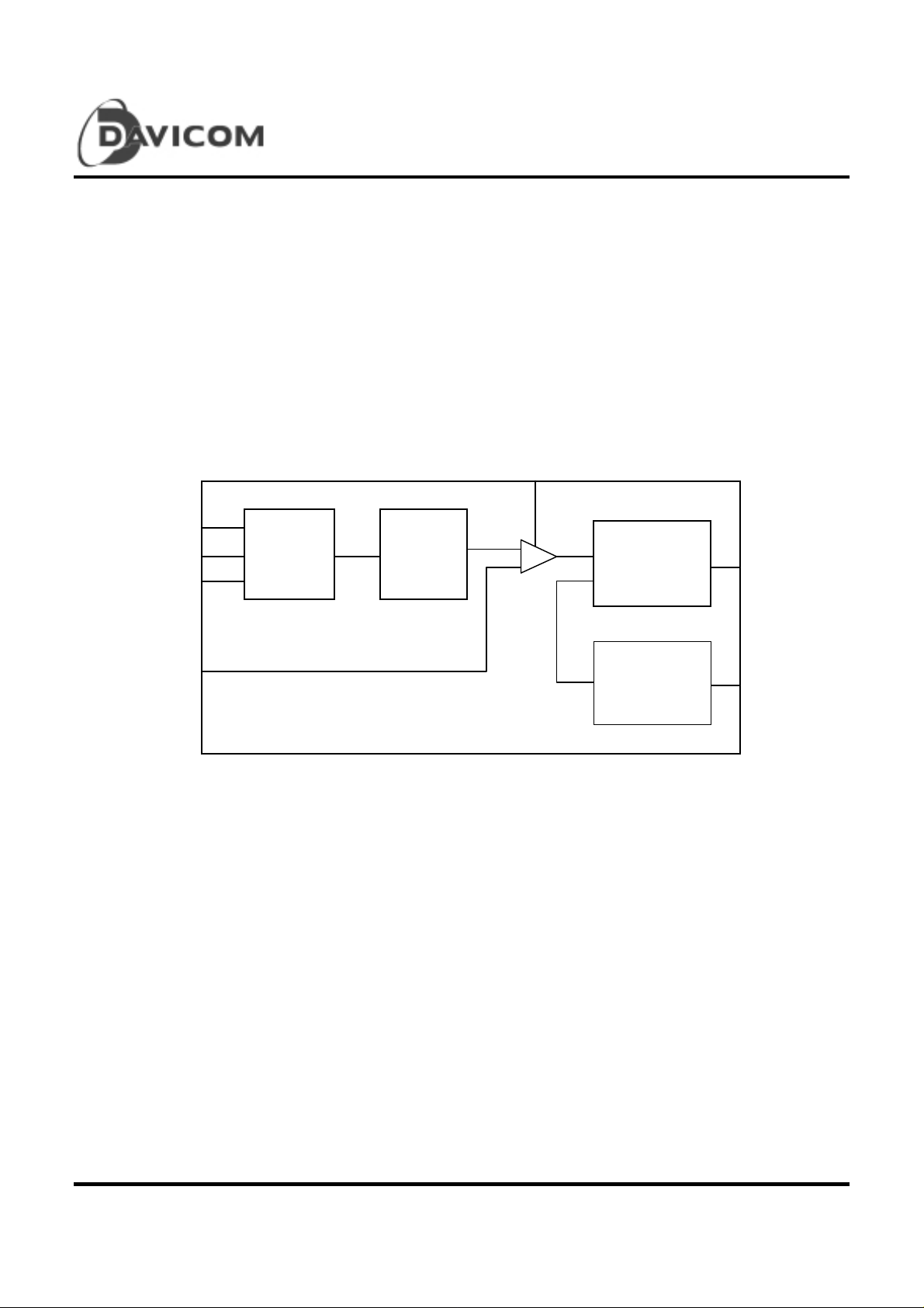
DM6383 Description
DM336P
The DM6383 Modem Control Unit (MCU) is designed
for use in high speed internal and external modem
applications. Its interface is compatible with the
DM6381/DM6382 Transmit and Receive Digital
Signal Processor Chipset. The DM6383 incorporates
a micro-cont r oller 80C31, virtual 16550A UART (with
FIFO mode), I/O and Plug & Play control logic. The
DM6383 Block Diagram
PC Data Bus
PC Address Bus
IRQ & R/W Control
RS 232 Interface
PnP Control
Logic
Virtual 16550
UART
DM6383 MCU performs the general modem control
fu nctions. It is also designed to provide Plug and Play
capabilit y for IS A bus systems by implementing PnP
control logic. The PnP logic supports hardware &
software selectable options to allow users to
configure the internal modem card without jumpers.
Mode Selection
8031
Micro-Controller
I/O Control Logic
External ROM,
RAM Interface
Modem Control
Interface
DM6383 Features
• Control interface support
• Supports parallel and serial i nterfaces
• Includes a micro-controller 80C31
• Maximum access 128K bytes external program
memory
• Maximum access 64K bytes external data memory
• Provides automatic con figuration capability to
Industry
• Configuration selectable by software
• Interrupt lines selec table
• I/O base conflict avoidable
4 Final
• Includes a virtual 16550A UART compatible parallel
interface
• Fully programmable serial interface:
- 6- , 7- or 8-bit characters
- Even, odd, or no-parity bit generation and
detection
- 1 and 2 stop bit gener ation
- Baud rate generation
• Includes I/O control logic f or modem control
interface
Version: DM336P- DS-F02
August 15, 2000
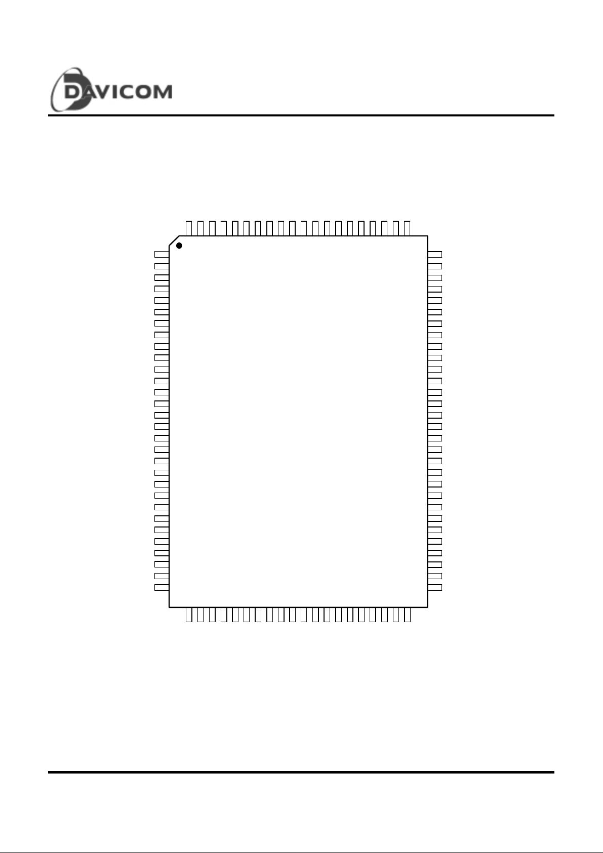
DM6383 Pin Configuration
DM336P
V.34 Integrated Data/ Fax/Voice/Speakerphone Modem Device Set
UD0
UD1
UD2
UD3
UD4
UD5
UD6
UD7
/IOR
GND
/IOW
/AEN
A11
A10
A9
A8
A7
A6
A5
A4
A3
A2
A1
A0
V
DD
IRQ4
IRQ5
IRQ7
IRQ10
RESET
1
2
3
4
5
6
7
8
9
10
11
12
13
14
15
16
17
18
19
20
21
22
23
24
25
26
27
28
29
30
DD
V
100
31
PS1
TEST1
98
99
33
32
GND
/TUCS
96
97
35
34
A15
/PNPEN
94
95
A14
93
A13
92
91
90
SEL1
89
SEL2
A12
DM6383F
36
37
38
39
424041
/POR
88
43
TXRCLK
RXRCLK
86
87
45
44
GND
85
46
D0
84
47
D1
83
48
D2
82
49
D3
81
50
80
79
78
77
76
75
74
73
72
71
70
69
68
67
66
65
64
63
62
61
60
59
58
57
56
55
54
53
52
51
D4
D5
D6
D7
CA0
CA1
CA2
CA3
CA4
CA5
CA6
CA7
GND
CA8
CA9
CA10
CA11
CA12
CA13
CA14
CA15
IRQ3
/RD
/WR
/PSEN
ALE/P
TXD
RXD
V
DD
P1.7
XTAL2
XTAL1
IRQ12
IRQ11
DD
V
IRQ15
TEST2
EAB/VP
CA16
/RUCS
GND
T0
T1
/RI
P1.1
P1.2
P0.0
P1.4
P1.5
P1.6
Final 5
Version: DM336P- DS-F02
August 15, 2000

V.34 Integrated Data/ Fax/Voice/Speakerphone Modem Device Set
DM6383 Pin Description
Pin No. Pin Name I/O Description
1 - 8 UD0 - UD7 I/O Data Bus Signal, in internal modem:
These signals are connected to the data bus of the PC I/O slot.
They are used to transfer data between the PC and the DM6383.
Modem Control Output, in external Modem:
Memory address mapping of the contr oller is E800H.
9 /IOR I I/O Rea d:
An active low signal used to read data from the DM6383.
10 GND P Ground
11 /IOW I I/O Writ e :
An active low signal used to write data to DM6383.
12 /AEN I Address Enable:
This is an active low signal to enable the system address for
DM6383.
13 - 24 A11 - A0 I System Address:
These signals are connected to the bus of PC I/O slot. They are
used to select DM6383 I/O ports.
25, 36, 52,
100
26, 27, 28,
29, 33 - 35
30 RESET I Reset:
31 XTAL1 I Crystal Oscillator Input
32 XTAL2 O Crystal Oscill ator Output
37 TEST2 I Test Pin (see description of pin 99)
38 EAB/VP I External ROM Select:
39 /RUCS O RX DSP Register Select Output:
40 CA16 O Bank Switch Control:
41, 68, 85, 96 GND P Ground
42 T0 I Controller Counter 0 Input
43 T1 I Controller Counter 1 Input
44 /RI I Ring Signal Input
45, 46,
48 - 51
VDD P +5V Power Supply
IRQ4, IRQ5,
IRQ7, IRQ10,
IRQ11, IRQ12,
IRQ15
P1.1, P1.2,
P1.4 - P1.7
O Interrupt Request:
These are 8 interrupt request pins. Only one pin, which i s decoded
from Configuration Register, can be activated, the other pins are
left floating. The active pin will go high when an interrupt request i s
generated from the DM6383.
An active high signal used to power-on reset the DM6383.
Should be connected to low state.
Memory address mapping of the contr oller is E400H.
This signal is used to sw itch external program memory between
bank 0 (lower 64K bytes) and bank 1 (upper 64K bytes) when the
EPROM for system use is 27010 (128Kx8 bits). Otherwise, this pin
is not connected.
I/O Controller Port 1 I/O
DM336P
6 Final
Version: DM336P- DS-F02
August 15, 2000
DM336P
V.34 Integrated Data/ Fax/Voice/Speakerphone Modem Device Set
DM6383 Pin Description (continued)
Pin No. Pin Name I/O Description
47 P0.0 O Modem Contr o l Output (memory map i s bit 4 of DAA)
53 RXD I Controller Serial Port Data Input
54 TXD O Controller Serial P ort Data Output
55 ALE/P O Controller Address Latch Enable:
Output pulse for latching the low byte of the address during
accesses to the extern al memory.
56 /PSEN O Controller Progr am Store Enable :
This output goes low during a fetch from external program memory.
57 /WR O Controller External Data Memory Write Control
58 /RD O Controller Extern al Data Memory Read Control
59 IRQ3 O Interrupt Request (see description of pin 26)
60 - 67 CA15 - CA8 O Controller Address Bus
69 - 76 CA7 - CA0 O Controller Address Bus
77 - 84 D7 - D0 I/O Controller Data Bus
86 TXRCLK I Transmitter Baud Rate Clock Input (Controller INT 0)
87 RXRCLK I Receiver Baud Rate Clock Input (Controller INT 1)
88 /POR O DSP Reset Output
89, 90 SEL1, S E L2 O Modem Co ntro l Out put (Memory map is bit 1-2 of DAA at memory
address D000H)
91 - 94 A12 - A15 I System Address:
These signals are connected to the bus of the PC I/O slot. They are
used to select the DM6383 I/O ports.
95 /PNPEN I PnP Mode Enable:
This pin will be detected to enable/disable the PnP mode. When it
is pulled down by a resistor (3.3K ~ 4.7K), the DM6383 can enter
the PnP mode when it receives the PnP initial key sequence. When
disconnected, an internal pull up will disable the Plug and Play
function.
97 /TUCS O TX DSP Register Select Output:
Memory address mapping of the contr oller is F000H.
98 PS1 O Modem Control Port Select Output:
Memory address mapping of the contr oller is D800H.
99 TEST1 I Test Pin: Used for system configuration and test mode
TEST2
0
0
1
1
Final 7
Version: DM336P- DS-F02
August 15, 2000
TEST1
0
1
0
1
System Configuart io n
Internal mode
External mode
Test mode
Test mode
V.34 Integrated Data/ Fax/Voice/Speakerphone Modem Device Set
DM6383 Functional Description
DM336P
1. Operating Mode Selection
The DM6383 MCU can be used with both internal and
external modems. When it works within an internal
modem, pin TEST2 and TEST1 must be in a low state.
The DM6383 includes a virtual UART and supports a
paralle l in t e rfa c e .
When DM6383 works within an external modem, pin
TEST2 must be in a low state, and pin TEST1 must
be in high. The virtual UART will be disabled and the
RS232 serial interface, enabled.
TEST2 TEST1 System Configuration
LOW LOW Internal Modem
LOW HIGH External Modem
HIGH X Test Mode
2. Micro-control ler (80C31) Reference
DM6383 supports a bank switch control pin to switch
external program memory between lower 64K bytes
(bank 0) and upper 64K bytes (bank 1) of 27C010.
In this mode, two instructions must be included in
software to switch bank 0 to bank 1:
i.e.,
CLR P1.3
JMP BANK 1 ADDRESS
With the same way, it can also switch back to bank 0
by
SETB P1.3
JMP BANK 0 ADDRESS
The clock source of the virtual UART logic is fixed at
1.8432MHz. The clock is derived from the external
crystal used by the DM6383 controller. Therefore, the
UART 1.8432MHz c lock must be obtained through
division. When the operating frequency of the
DM6383 controller changes, the divider should be
changed accordingly. This divider is specif ie d by the
Configuration Register which can be written by the
DM6383 controller. The address mapping of the
register is D4000H: ( DM 6383 cont r oller memory
mapping)
Bit 0: Always 0.
Bit 6-1: B6 - B1 define the clock divider range from 2
to 64 (even number).
Bit 7: Not used.
b. UART Baud Generator Divisor Latch Register:
Address EC00H
Read only
bit7 bit6 bit5 bit4 bit3 bit2 bit1 bit0
dat7 dat6 dat5 dat4 dat3 dat2 dat1 dat0
By reading this register, the micro-controller can
monitor the value of the low byte divisor latch of the
virtual UART baud generator (see DLL in next section)
and determine the baud rate clock itself.
c. Modem Status Controller Register (MSCR):
Address E000H
* For detailed information about mi cro-controller,
please see Programmer's Guid e to 8031.
3. Micro-controller Register Description
a. UART Clock Register :
Address D4000H Reset State: 06H
Write Only
bit7 bit6 bit5 bit4 bit3 bit2 bit1 bit0
X dat6 dat5 dat4 dat3 dat2 dat1 0
8 Final
Write only
bit7 bit6 bit5 bit4 bit3 bit2 bit1 bit
0
0000/CTS/DSR/DCD/RI
The advantage of this register is that the modem line
status information can be passed to the virtual UART
by the micro-controller. The resulting signals are Ring
Detect (/RI), Carrier Detect (/DCD) , Data Set Ready
(/DSR) and Clear To Send (/CTS).
Version: DM336P- DS-F02
August 15, 2000
V.34 Integrated Data/ Fax/Voice/Speakerphone Modem Device Set
d. Modem Outp ut Port Register: Address D000H
Write only
bit7 bit6 bit5 bit4 bit3 bit2 bit1 bit0
PO0 SEL2 SEL1 /POR
These 4 bits work as output ports in response to the
88th, 89th, 90th and 47th pins of this chip (see pin
description).
DM336P
* When reset condition occurred, the I/O and Interrupt
configuration registers must be reset to default
value according to bit 0 - bit 5.
4. UART(16550A) Emulat io n Registers
a. Receiver Buffer (Read), Transmitter Holding
Register (Write)
e. PnP Isolation & Resource Data Port: Address
F800H
Write only
The PnP isolation and resource data can be bytesequentially written to the corresponding memory
(built-in SRAM) through this register.
f. Auto-configu rat io n Register: Address F400H
bit2 bit1 bit0 IRQ bit5 bit4 bit3 I/O
0 0 0 3 0 0 0 03F8-03FF(COM1)
0 0 1 4 0 0 1 02F8-02FF(COM2)
0 1 0 5 0 1 0 03E8-03EF(COM3)
0 1 1 7 0 1 1 02E8-02EF(COM4)
1 0 0 10 1 0 0 03F0-03F7(COM5)
1 0 1 11 1 0 1 02F0-02F7(COM6)
1 1 0 12 1 1 0 03E0-03E7(COM7)
1 1 1 15 1 1 1 02E0-02E7(COM8)
The default I/O base and IRQ data stored in 94C46
should be loaded to this register by micro-controller,
and then enable the default configuration. Microcontroller can also get the current I/O base and IRQ
information by a read from thi s regist e r.
The configuration determined by this register should
be disabled when the register detects the Initiation
Key described in the next section.
Bit 6: When this bit is set to inform micro-controller
that the current I/O base and IRQ data should
be stored to 93C46 as the default setting at the
next power-on reset through programming the
Auto-configuration Register, this bit should be
cleared by micro-controlle r.
Address: 0 (DLAB=0) Reset State 00h
bit7 bit6 bit5 bit4 bit3 bit2 bit1 bit0
dat7 dat6 dat5 dat4 dat3 dat2 dat1 dat0
When this register address is read, it contains t he
parallel received data. Data to be transmitted is
written to this registe r .
b. Interrupt Enable Register (IER): Address 1
Reset State 00h, Write Only
bit7 bit6 bit5bit4 bit3 bit2 bit1 bit0
0 0 0 0 Enable
Mode
mStatu
This 8-bit register enables the four types of interrupts
as described below. Each interrupt source can
activate the INT output signal if enabled by this
register. Resetting bits 0 through 3 will disable all
UART interrupts.
Bit 0: This bit enables the Received Data Available
Interrupt (and timeout interrupts in the FIFO
mode) when set to logic 1.
Bit 1: This bit enables the Transmitter Holding
Register Empty Interrupt when set to logic 1.
Bit 2: This bit enables the Receiver Line Status
Interrupt when set to logic 1.
s
Intr
Enable
Line
Status
Intr
Enable
TX
Holdin
g
Regist
er
Intr
Enable
RX
Data
Intr
Bit 7: When bit 7 is set, it enables hardware
configuration set according to bit 0-bit 5
(Jumper mode) and load the proper value of
PnP Registers including I/O and Interrupt
Configuration Registers. This bit will be reset,
when it receiv es PnP I nitial Key sequence.
Final 9
Version: DM336P- DS-F02
August 15, 2000
Bit 3: This bit enables the MODEM Status Interrupt
when set to logic 1.
Bit 4-7: Not used

DM336P
V.34 Integrated Data/ Fax/Voice/Speakerphone Modem Device Set
c. Interrupt Identification Register (IIR): Address 2
Reset State 01h, Read only
bit7 bit6 bit5 bit4 bit3 bit2 bit1 bit0
FIFO
Enable
In order to provide minimum software overhead
during data transfers, the virtual UART prioritizes
interrupt s into four levels as followed: Receiver Line
Status (priority 1), Receiver Data Available (priority 2),
Character Timeout Indication (priority 2, FIFO mode
only), Transmitter Holding Register Empty (priority 3 ),
and Modem Status (priority 4).
The IIR register gives prioritized information as to the
status of interrupt conditions. When accessed, the IIR
indicates the highest priority interrupt that is pending,
as indicated by bi ts INT D( 2- 0) .
D3 D2 D1 D0 Priority Level Interrup t T ype Condition Reset
0001 - - - 0 1 1 0 Highest Receiver Line
0 1 0 0 Second Receiver Data
1 1 0 0 Second Character
0 0 1 0 Third Transmitter
0 0 0 0 Four th Modem Status Clear to Send, Data Set
000D3:
INTD2
D2:
INTD1
D1:
INTD0
Status
Available
Timeout
Indication
Holding Register
Empty
D0:
int
Pending
Bit 0: This bit can be used in either a prioritized
interrupt or polled environment to indicate
whether an interrupt is pending. When this bit is
a logic 0, an interrupt is pending, and the IIR
contents may be used as a pointer to the
appropriate interrupt service routine. When bit 0
is a logic 1, no interrupt is pending, and pol ling
(if used) continues.
Bit 1-2: These two bits of the IIR are used to identify
the highest priority interrupt pending, as
indicated in the table below.
Bit 3: In character mode, this bit is 0. In FIFO mode,
this bit is set, along with bit 2, when a timeout
interrupt is pending.
Bit 4-6: Not used
Bit 7: This bit is set when FCR0 = 1.
Overrun Error, Pari ty
Error, Framing Error or
Break Interrupt
Receiver Data Available
or Trigger Level Reached
No characters have been
read from or written to the
Rx FIFO during
programming time
interval, and the Rx FIFO
is not empty
Transmitter Holding
Register Empty
Ready, Ring Indi c ator or
Data Carrier Detected
Reads the Line Status
Register
Reads the Receiver
Buffer Register or the
FIFO Drops Below The
Threshold Value
Reads The Receiver
Buffer Register
Reads the IIR Register or
(if source of interrupt)
Writes To The Transmitter
Holding Register
Reads the Modem Status
Register
10 Final
Version: DM336P- DS-F02
August 15, 2000
DM336P
V.34 Integrated Data/ Fax/Voice/Speakerphone Modem Device Set
d. FIFO Control Register (FCR): Address 2
Reset State 00h , write only
bit7 bit6 bit5bit4bit3 bit2 bit1 bit0
RCVR
(MSB)
This is a write only register at the same location as
the IIR, which is a read only register. This register is
used to enable the FIFOs, clear the the FIFOs, set the
RxFIFO trigger level, and select the type of DMA
signal.
Bit 0: Writing a 1 to FCR0 enables both transmit and
Bit 1: Writing a 1 to FCR1 clears all bytes in the
Bit 2: Writing a 1 to FCR2 clears all bytes in the
Bit 3: Setting FCR3 to 1 will cause the RXRDY and
Bit 4-5: Reserved
RCVR
Trig
Trig
(LSB)
receive FIFOs. Resetting FCR0 will clear all
bytes in both FIFOs. When changing from FIFO
mode to Character mode (and vice versa), data
is automatically cleared from the FIFOs.
RxFIFO and resets its counter logic to 0.
TxFIFO and resets its count er logic to 0.
TXRDY pins to change from mode 0 to mode 1
if FCR0 = 1.
00DMA
TxFIFO
Mode
Reset
RxFIFO
Reset
FIFO
Enabl
e
This register is available to maintain compatibility with
the standard 16550 register set, and provides
information to the internal hardware that is used to
determine the number of bits per character.
WLS1 WLS2 Word Length
005 bits
016 bits
107 bits
118 bits
Bit 0-1: WLS0-1 specif ies the number of bits i n each
transmitted and received serial character.
Bit 2: This bit specif ies the number of stop bits in
each transmitted character. If bit 2 is a logic 0,
one stop bit is generated in the transmitted data.
If bit 2 is a logic 1 when a 5-bit word length is
selected via bits 0 and 1, one and a half stops
are generated. If bit 2 is a lo gic 1 w hen either a
6-, 7- or 8-bit word length is select ed, two stop
bits are generated. The Receiver checks the
first Stop-bit only, regardless of the number of
Stop bits selected.
Bit 3: Logic 1 indicates that the PC has enabled the
parity generation and checking.
Bit 4: Logic 1 indicates that the PC is requesting an
even number of logic 1s to be transmitted or
checked. Logic 0 indicates that the PC is
requesting odd parity generation and checking.
Bit 6-7: FCR6, FCR7 are used to set the trigger level
for the RxFIFO i nterrupt.
FCR6 FCR7 RxFIFO Trigger Level
00 01
01 04
10 08
e. Line Control Register (LCR): Address 3
Reset State 00h, Write Only
bit7 bit6 bit5 bit4 bit3 bit2 bit1 bit0
DLAB SBRK STP EPS PEN STB WLS1 WLS0
Final 11
Version: DM336P- DS-F02
August 15, 2000
Bit 5: When bit 3, 4 and 5 are logic 1, the parity bit i s
transmitted and checked by the receiver as
logic 0. If bits 3 and 5 are 1 and bit 4 is logic 0,
then the parity is transmitted and checked as
logic 1.
Bit 6: This is a Break Control bit. When it is set to
logic 1, a break condition is indicated.
Bit 7: The Divisor Latch Access bit must be set to
logic 1 to access the Divisor Latches of the
baud generator during a read or write operation.
It must be set to logic 0 to access the Receiver
Buffer, the Transmitter Holding Register, or the
Interrupt E nable Register.

DM336P
V.34 Integrated Data/ Fax/Voice/Speakerphone Modem Device Set
f. Modem Control Register (MCR): Address 4
Reset State 00h
bit7 bit6 bit5 bit4 bit3 bit2 bit1 bit0
000000RTSDTR
Bit 0: This bit asserts a Data Terminal Ready
condition that is readable via port P1.1 of microcontroller 8031. When bit 0 is set to logic 1, the
P1.1 is forced to logic 0. When bit 0 is reset to
logic 0, the P1.1 is forced to logic 1.
Bit 1: This bit asserts a Request To Send condition
that is readable via port P3.4 of the microcontroller 8031. Bit 1 affects P3.4 in a manner
identical to that described above for bit 0.
g. Line Status Register (LSR): Address 5
Reset State 60h, Read only
bit7 bit6 bit5 bit4 bit3 bit2 bit1 bit0
RCV ETEMT THRE BI FE PE OE DR
This register prov ides status i nformation to the host
PC conc erning the data transfer. Bit 1-4 indicate the
error conditi ons that produce a Receiver Line Status
interrupt whenever any of the corresponding
conditions are detected. The Line Status Register is
intended for read operations only.
Bit 0: Set to l ogic 1 when a received charac te r is
availab le in the RxFIFO . This bit is reset to logic
0 when the RxFIFO is empty.
Bit 1: An Overrun error will occur only after the
RxFIFO is full and the next character has
overwritten the u nread FIFO data. This bit is
reset upon reading the Line Status Register.
Bit 3: This bit is the Framing Error (FE) indicator. Bit 3
indicates that the received character did not
have a valid stop bit. Bit 3 is set to a logic 1
whenever the stop bit following the last data bit
or parity bit i s detec ted as a zero bit (spacing
level). The FE bit is reset whenever the CPU
reads the contents of the Line S tatus Register.
The FE error condition is associated with the
particular character in the FIFO to which it
applies. This err or is revealed to the CPU when
its associated charact er is at the top of the
FIFO.h. Modem Status Register (M SR ):
Address 6 Reset State, bit 0- 3: low, bit 4-7:
input signal.
Bit 4: Thi s bit is a Break Interrupt (BI) indic ator. Bit 4
is set to logic 1 whenever the receiv ed data
input is held in the Spacing (logic 0) state for
longer than a full word transmission time (that is,
the total time of Start bit + data bits + Parity +
Stop bits). The BI indicator is reset whenever
the CPU reads the contents of the Line Status
Register. The BI error condition is associated
with the particular character in the FIFO to
which it applies. This error is revealed to the
CPU when its associated character i s at the top
of the FIFO.
Bit 5:This bit is a Transmitter Holding Register Em pty
indicator. Bit 5 indicates that UART is ready to
accept a new character for transmission. In
addition, t his bit c auses UART to issue an
interrupt to the CPU when the Transmit Holding
Register Empty Interrupt Enable is set high. The
THRE bit is reset to logic 0 when the host CPU
loads a character into the Transmit Holding
register. In the FIFO mode, this bit is set when
the TxFIFO is empty, and i s cleared when at
least 1 byte is written to the TxFIFO.
Bit 2: A value of logic 1 indicates that a received
character does not have the correct even or
odd parity as selected by the Even Parity Select
bit. This error is set when the corresponding
character i s at the top of the RxFIFO. It will
remain set until the CPU reads the LSR. This
Parity Error indication is associated with the
particular character in the FIFO to which it
applies. This err or is revealed to the CPU when
its associated charact er is at the top of the
FIFO.
12 Final
Bit 6: This bit is the Tran s mitte r E mpt y indicator. Bit 6
is set to a logic 1 whenever the Transmitter
Holding Register (T HR ) i s em pty, and is reset to
a logic 0 whenever the THR contains a
character. In FIFO mode, this bit is set to 1
whenever the tr ansmitter FIFO is empty.
Bit 7: In character mode, this bit is 0. In FIFO mode,
this bit is set when there is at l east one parity
error, framing error, or break indication in the
FIFO. If there are no subsequent errors in the
FIFO, LSR7 is cleared when the CPU reads the
LSR.
Version: DM336P- DS-F02
August 15, 2000