FEATURES
• 8-Bit flash A/D converter
• 20MHz sampling rate
• Complete support circuitry
• Low power, 1.5W
• 7MHz full power bandwidth
• Sample-hold not required
• Three-state outputs
• MIL-STD-883 versions
GENERAL DESCRIPTION
The ADC-228 combines analog front-end circuitry and a flash
A/D converter to digitize high-speed analog signals at a rate of
20 million samples per second. The ADC-228 contains an
8-bit, 20MHz, flash A/D, a wideband analog input buffer, a
precision voltage reference, temperature compensation
circuitry, reference trims, and a three-state output buffer in a
24-pin package.
The ADC-228 offers significant savings by combining all of the
circuitry in a single package. Valuable board real estate is
saved, and design time and manufacturing costs are reduced.
The ADC-228 is housed in a 24-pin ceramic DDIP package
and is available in the commercial, 0 to +70°C, or military,
–55 to +125°C, temperature ranges. A MIL-STD-883 version
is also available. Operation is from ±15V and +5V power
supplies.
INNOVATION and EX C ELL E N C E
® ®
ADC-228
8-Bit, 20MHz, Complete
Flash A/D Converter
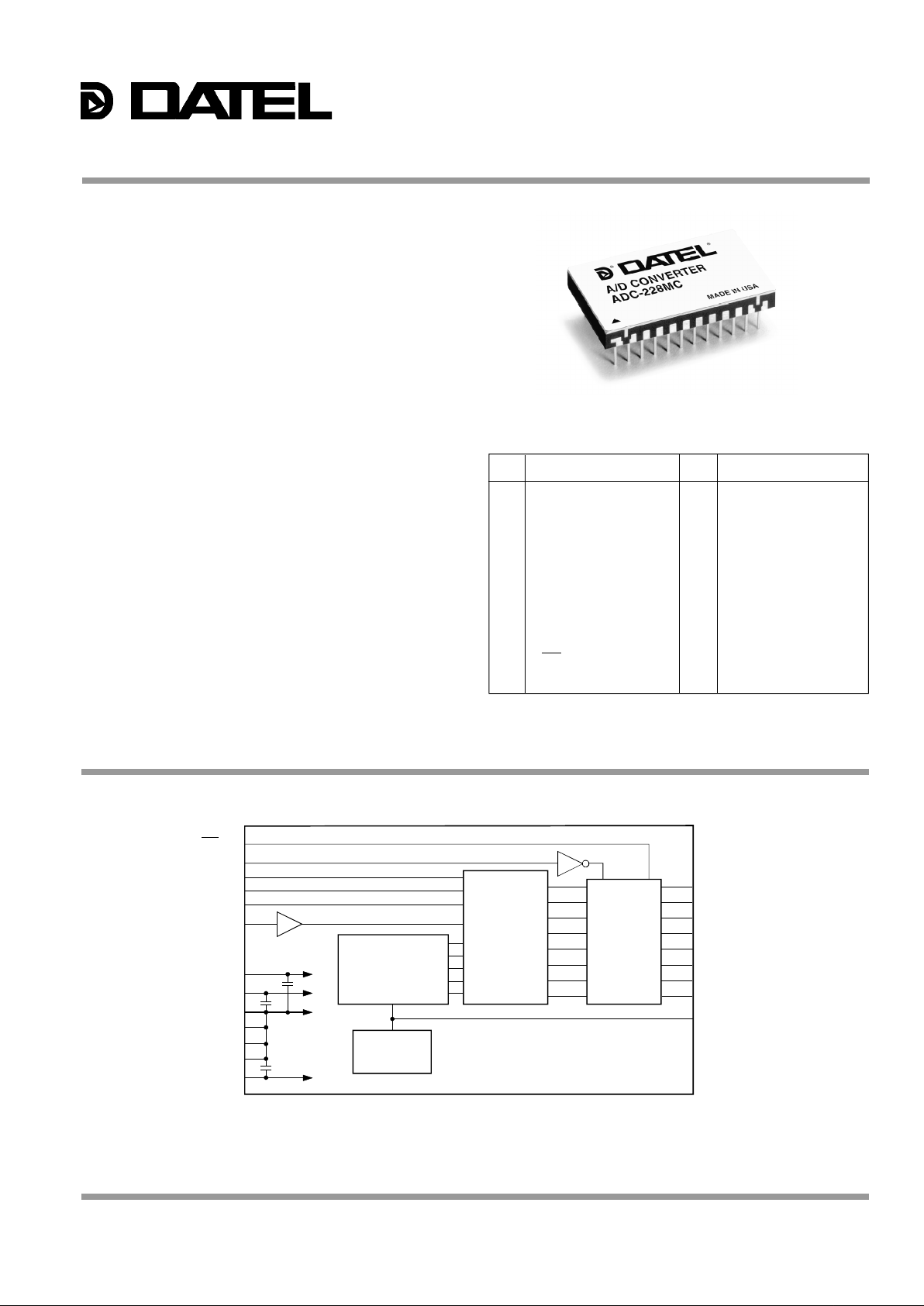
Figure 1. Functional Block Diagram
PIN FUNCTION PIN FUNCTION
1 +5V SUPPLY 24 BIT 8 (LSB)
2 GROUND 23 BIT 7
3 +5V REFERENCE OUT 22 BIT 6
4 GROUND 21 BIT 5
5 ANALOG INPUT 20 NO CONNECTION
6 GROUND 19 +15V SUPPLY
7 GROUND 18 CLOCK INPUT
8 NLINV 17 BIT 4
9 NMINV 16 BIT 3
10 –15V SUPPLY 15 BIT 2
11 CS1 14 BIT 1 (MSB)
12 CS1 13 NO CONNECTION
INPUT/OUTPUT CONNECTIONS
13 NO CONNECTION
20 NO CONNECTION
14 BIT 1 (MSB)
15 BIT 2
16 BIT 3
17 BIT 4
21 BIT 5
22 BIT 6
23 BIT 7
24 BIT 8 (LSB)
3 +5V REF. OUT
TRI-STATE
BUFFER
8-BIT
20MHz
FLASH
CONVERTER
LINEARIZATION
& TEMPERATURE
COMPENSATION
NETWORK
INPUT
BUFFER
CS1 11
CS1 12
NLINV 8
NMINV 9
CLOCK 18
ANALOG INPUT 5
+15V SUPPLY 19
GROUND 4
GROUND 7
GROUND 6
–15V SUPPLY 10
+5V SUPPLY 1
VOLTAGE
REFERENCE
NETWORK
GROUND 2
DATEL, Inc., 11 Cabot Boulevard, Mansfield, MA 02048-1151 (U.S.A.) • Tel: (508) 339-3000 Fax: (508) 339-6356 • For immediate assistance (800) 233-2765

ADC-228
® ®
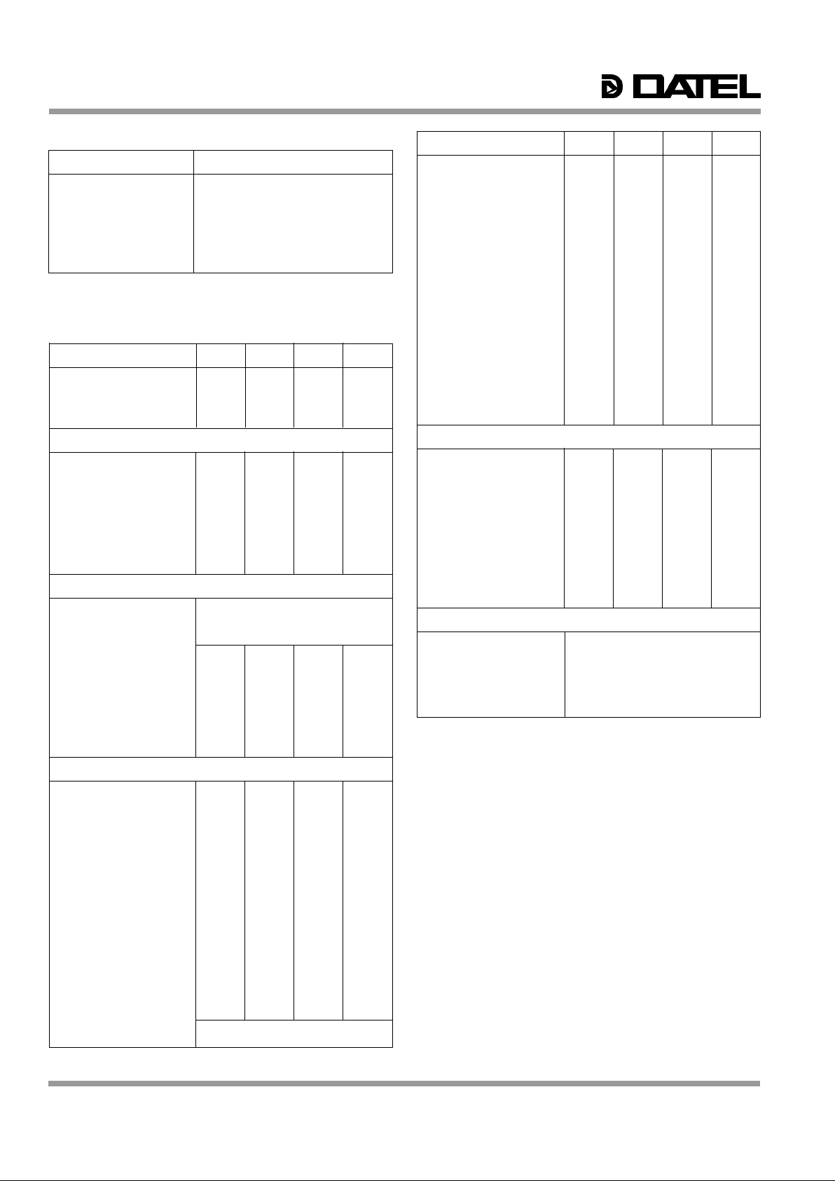
FUNCTIONAL SPECIFICATIONS
(Apply over the operating temperature range with 20MHz clock and ±15V and +5V
power supply voltages, unless otherwise specified.)
ANALOG INPUTS MIN. TYP. MAX. UNITS
Single-Ended, Non-Isolated
Input Range, dc-20MHz 0 — +5.0 Volts
Input Resistance 2.45 2.5 2.55 kΩ
Input Capacitance — 5 10 pF
DIGITAL INPUTS
Logic Levels
Logic 1 +2.0 — — Volts
Logic 0 — — +0.8 Volts
Logic Loading
Logic 1 — — +160 µA
Logic 0 — — –0.5 mA
Clock Pulse Widths
"High" 25 — — ns
"Low" 19 — — ns
DIGITAL OUTPUTS
Coding
Resolution
Logic Levels
Logic 1 +2.4 — — Volts
Logic 0 — — +0.4 Volts
Logic Loading
Logic 1 — — –1 mA
Logic 0 — — +1 mA
Output Data Valid Delay
From Rising Edge — 30 40 ns
Output Hold Time 5 — — ns
PERFORMANCE
Sampling Rate ➀ 20 — — MHz
Differential Linearity ➁
Code Transitions — ±0.5 ±0.75 LSB
Code Centers — ±0.25 ±0.5 LSB
Integral Linearity, +25°C
End-point — ±0.5 ±0.75 LSB
Best-fit Line — ±0.35 ±0.5 LSB
Over Temperature End-point — — ±1 LSB
Best-fit Line — — ±1 LSB
Zero-Scale Offset
Code "0" to "1" Transition
+25°C — — ±0.5 LSB
–55 to +125°C — ±0.5 ±1.5 LSB
Gain error — ±0.5 ±1.5 LSB
Full Scale Absolute Accuracy — ±0.5 ±1.5 LSB
Differential Gain ➂ — 2 — %
Differential Phase ➂ — 1 — deg.
Aperture Delay — 8 — ns
Aperture Jitter — 50 — ps
No Missing Codes
Power Supply Rejection
DYNAMIC PERFORMANCE MIN. TYP. MAX. UNITS
Total Harm. Distortion, –0.5dB
DC to 2.5 MHz — –55 –53 dB
2.5 MHz to 5 MHz — –50 –48 dB
5 MHz to 10 MHz — –39 –36 dB
Signal-to-Noise Ratio
and Distortion, –0.5dB
DC to 2.5 MHz 44 49 — dB
2.5 MHz to 5 MHz 43 46 — dB
5 MHz to 10 MHz 35 38 — dB
Signal-to-Noise Ratio
w/o Distortion, –0.5 dB
DC to 2.5 MHz 45 48 — dB
2.5 MHz to 5 MHz 45 48 — dB
5 MHz to 10 MHz 42 45 — dB
Effective Bits, –0.5dB
DC to 2.5 MHz 7.1 7.75 — Bits
2.5 MHz to 5 MHz 6.9 7.4 — Bits
5 MHz to 10 MHz 5.6 6.1 — Bits
Input Bandwidth
Full Power 7 — — MHz
Small Signal (–20dB) 40 — — MHz
POWER SUPPLY
Power Supply Range
+15V Supply +11 +15 +15.75 Volts
–15V Supply –11 –15 –15.75 Volts
+5V Supply +4.75 +5 +5.25 Volts
Power Supply Current
+15V Supply — — +30 mA
–15V Supply — — –10 mA
+5V Supply — — +230 mA
Power Dissipation
±12V, +5V Nominal — 1.4 1.65 Watts
Over full supply range — 1.6 1.85 Watts
±15V, +5V Nominal — 1.5 1.75 Watts
PHYSICAL/ENVIRONMENTAL
Operating Temp. Range, Case
ADC-228MC 0 to +70°C
ADC-228MM, ADC-228/883 –55 to +125°C
Storage Temp. Range –65 to +150°C
Package Type 24-pin, ceramic DDIP
Weight 0.3 ounces (8.5 grams)
Footnotes:
➀ At full power input and chip selects enabled.
➁ See Technical Note 3.
➂ For 10-step, 40 IRE NTSC ramp test.
ABSOLUTE MAXIMUM RATINGS
PARAMETER LIMITS
Power Supply Voltage, Pin 1 –0.5 to +7V
Pin 19 –0.3 to +18V
Pin 10 +0.3 to –18V
Digital Inputs, Pins 8,9,11,12,18 –0.5 to +5.5V
Analog Input, Pin 5 –6 to +7.5V
Digital Outputs –0.5 to +5.5V (short circuit protected to ground)
Lead Temp. (10 seconds) +300°C
Over the operating temperature range
±0.02% FSR/%V
S
maximum
Straight bin., comp. bin., two's
comp.,
comp. two's comp.
8 bits
2
 Loading...