

DATEL ADC-321 Datasheet
® ®
DATEL, Inc., Mansfield, MA 02048 (USA.) • Tel: (508)339-3000, (800)233-2765 Fax: (508)339-6356 • Email: sales@datel.com • Internet: www.datel.com
ADC-321
8-Bit, 50MHz
Video A/D Converter
1 BIT 8 (LSB) 32 NO CONNECTION
2 BIT 7 31 DIGITAL GROUND (DGND)
3 BIT 6 30 OUTPUT ENABLE (OE)
4 BIT 5 29 CLAMP ENABLE (CLE)
5 BIT 4 28 DIGITAL GROUND (DGND)
6 BIT 3 27 CLAMP CONTROL (COP)
7 BIT 2 26 CLAMP REF. (V
REF)
8 BIT 1 (MSB) 25 REF. BOTTOM SENSE (V
RBS)
9 TEST 24 REF. BOTTOM (V
RB)
10 +DV
S (Digital) 23 ANALOG GROUND (AGND)
11 TEST 22 ANALOG GROUND (AGND)
12 A/D CLOCK 21 ANALOG IN (V
IN)
13 NO CONNECTION 20 +AV
S (Analog)
14 NO CONNECTION 19 +AV
S (Analog)
15 CLAMP IN (CLP) 18 REF. TOP (V
RT)
16 +AV
S (Analog) 17 REF. TOP SENSE (VRTS)
FEATURES
• Low power dissipation (180mW max.)
• Input signal bandwith (100MHz)
• Optional synchronized clamp function
• Low input capacitance (15pF typ.)
• +5V or +5V/+3.3V power supply operation
• Differential nonlinearity (±½LSB max.)
• Optional self-biased reference
• CMOS/TTL compatible inputs
• Outputs 3-state TTL compatible
• Surface mount package
GENERAL DESCRIPTION
The ADC-321 is an 8-bit, high speed, monolithic CMOS, subranging A/D converter. The ADC-321 achieves a sampling rate
comparable to flash converters by employing a sub-ranging
technique which uses multiple comparator blocks each
containing a sample-and-hold amplifier. The ADC-321 can
operate with either a single +5V or dual +5V and +3.3V power
source to allow easy interfacing with 3.3V logic.
An optional synchronous clamp function useful for video signal
processing is provided. The ADC-321 is well suited for the
portable video signal processors due to its low 125mW typical
power dissipation. The ADC-321 also features ±0.5 LSB max.
differential non-linearity, a self bias function that can eliminate the
need for external references, SNR with THD of 45dB, a small
32-pin QFP package and an operating temperature range
of –40 to +85°C
INPUT/OUTPUT CONNECTIONS
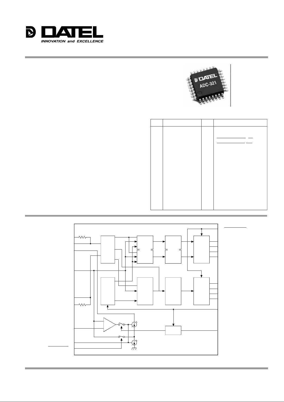
Figure 1. ADC-321 Functional Block Diagram
PIN FUNCTION PIN FUNCTION
1 BIT 8 (LSB)
2 BIT 7
3 BIT 6
4 BIT 5
Reference
Supply
4-Bit
Lower
Sampling
Comparator
A
B
Clock
Generator
4-Bit
Upper
Sampling
Comparator
4-Bit
Lower
Encoder
A
B
4-Bit
Upper
Encoder
Upper
Data
Latch
Lower
Data
Latch
–
+
D-FF
31 DGND
30 OUTPUT ENABLE
5 BIT 4
6 BIT 3
7 BIT 2
8 BIT 1 (MSB)
12 A/D CLOCK
15 CLAMP IN
9 TEST (Open)
10 +DV
S
11 TEST (Open)
16
17
18
19
2120V
IN
+AVS
+AV
S
V
RT
+AVS
V
RTS
22AGND
23AGND
24V
RB
25V
RBS
26V
REF
27CLAMP CONTROL
29CLAMP ENABLE
28DGND

ADC-321
2
® ®
DIGITAL OUTPUTS (continued) MIN. TYP. MAX. UNITS
Output Data Delay
(OE = 0V, C
L = 15pF)
(@ +DV
S = +5V) tPLH 5.5 9.5 12.0 ns
t
PHL 5.5 8.5 12.0 ns
(@+DV
S = +3.3V) tPLH 4.3 11.8 16.3 ns
t
PHL 4.3 7.6 16.3 ns
3-State Output Enable Time ➆
(R
L = 1kΩ, CL = 15pF)
(@ +DV
S = +5V) tPZH 2.5 4.5 8.0 ns
t
PZL 2.5 6.0 8.0 ns
(@+DV
S = +3.3V) tPZH 3.0 7.0 9.0 ns
t
PZL 3.0 5.0 9.0 ns
3-State Output Disable Time ➇
(R
L = 1kΩ, CL = 15pF)
(@+DV
S = +5V) tPHZ, tPLZ 3.5 5.5 7.5 ns
(@+DV
S = +3.3V) tPHZ, tPLZ 2.5 5.5 8.0 ns
CLAM CIRCUIT
Clamp Offset Voltage ➈ 0 20 40 mV
Clamp Pulse Width ➉ 1.75 2.75 3.75 µA
PERFORMANCE
Resolution 8 — — Bit
Sampling Rate, maximum, F
S 50 — — MHz
minimum, F
S — — 0.5 MHz
Aperature Delay (Tds) — 0 — ns
Integral Linearity Error — ±0.7 ±1.5 LSB
Diff. Linearity Error — ±0.3 ±0.5 LSB
Diff. Gain Error — 3 — %
Diff. Phase Error — 1.5 — deg
S/N Ratio with THD
(f
IN = 100kHz) — 45 — dB
(f
IN = 500kHz) — 44 — dB
(f
IN = 1MHz) — 44 — dB
(f
IN = 3MHz) — 43 — dB
(f
IN = 10MHz) — 38 — dB
(f
IN = 25MHz) — 32 — dB
Spurious Free Dynamic Range
(f
IN = 100kHz) — 51 — dB
(f
IN = 500kHz) — 46 — dB
(f
IN = 1MHz) — 49 — dB
(f
IN = 3MHz) — 46 — dB
(f
IN = 10MHz) — 45 — dB
(f
IN = 25MHz) — 45 — dB
POWER REQUIREMENTS
Power Supply
+AV
S +4.75 +5.0 +5.25 Volts
+DV
S +3.0 — +5.5 Volts
|AGND – DGND| 0 — 100 mW
Power Supply Current
1. AI
S, DIS (@ +DVS = +5V) — 25 36 mA
2. AI
S — 23 33 mA
DI
S (@ +DVS = +3.3V) — 2 3 mA
Power Dissipation — 125 180 mW
ENVIRONMENTAL/PHYSICAL
Operating Temp. Range, Case –40 — +85 °C
Storage Temperature Range –55 — +150 °C
Package Type 32-pin, plastic QFP
Weight 0.007 ounces (0.2 grams)
ANALOG INPUTS MIN. TYP. MAX. UNITS
Input Voltage Range ➀ +0.5 — +2.5 Volts
Input Capacitance
(@ V
IN = +1.5Vdc +0.07VRMS) — 15 — pF
Input Signal Bandwidth
–1dB (@ R
IN = 33Ω) — 60 — MHz
–3dB (@ R
IN = 33Ω) — 100 — MHz
REFERENCE INPUTS
Reference Resistance
V
RT – VRB 260 370 480 Ω
Reference Current 4.1 5.4 7.7 mA
Reference Voltage
V
RT — — +2.7 Volts
V
RB 0 — — Volts
V
RT – VRB 1.7 — — Volts
Self Bias Voltage ➁
V
RB +0.52 +0.56 +0.60 Volts
V
RT – VRB 1.80 1.92 2.04 Volts
Capacitance (V
RT, VRTS, VRB, VRBS) — — 11 pF
Offset Voltage
V
RT –70 –50 –30 mV
V
RB 20 40 60 mV
DIGITAL INPUTS
Logic Levels ➂
Input Voltage "1" 2.2 — — Volts
Input Voltage "0" — — +0.8 Volts
Input Current ➃
A/D CLK –240 — 240 µA
CLP, CLE –240 — 40 µA
OE –40 — 240 µA
Input Capacitance — — 11 pF
A/D Clock Pulse Width
(tpw1) 10 — — ns
(tpw0) 10 — — ns
DIGITAL OUTPUTS MIN. TYP. MAX. UNITS
Output Current (OE = 0V) ➄
(@ +DV
S = +5V) "1" — — –2 mA
"0" 4 — — mA
Output Current (OE = 0V) ➄
(@ +DV
S = +3.3V) "1" — — –1.2 mA
"0" 2.4 — — mA
Output Current ➅
(@ OE = +3V) "1" –40 — 40 µA
"0" –40 — 40 µA
Capacitance — — 11 pF
PARAMETERS LIMITS UNITS
Power Supply Voltage (+AV
S, +DVS) –0.5 to 7 Volts
Analog Input Voltage, (V
IN) –0.5 to +AVS + 0.5 Volts
Reference Input Voltage (V
RT, VRB) –0.5 to +AVS + 0.5 Volts
Digital Input Voltage (V
IH, VIL) –0.5 to +AVS + 0.5 Volts
Digital Output Voltage (V
OH, VOL) –0.5 to +DVS + 0.5 Volts
ABSOLUTE MAXIMUM RATINGS
FUNCTIONAL SPECIFICATIONS
Typical at TA = 25°C, VRT = +2.5V, VRB = +0.5V, +AVS = +5V, +DVS = +3V to +5.5V,
F
S = 50MHz unless otherwise specified.
(TA = +25°C)
Footnotes:
➀ See technical note 6
➁ Pin 25 tied to AGND and pin 17 tied to +AV
S
➂ +AVS = +4.75 to +5.25V and +DVS = 3 to +5.5V, full operating tem. range.
➃ V
IL = 0V and VIH = +AVS, full operating temp. range
➄ V
OH = +DVS–0.8V and VOL = +0.4V, full operating temp. range
➅ +DVS = +3 to +5.5V, full operating temp. range
➆ OE: +3 to 0V change
➇ OE: 0 to +3V change
➈ 2.75µs clamp pulse width, 14.3MHz sampling,
15.75kHz clamping rate
➉ The clamp pulse width given is for NTSC. For other processing
systems adjust the rate to the clamp pulse cycle (1/15.75kHz for
NTSC) to equal the value for NTSC.
NTSC 40IRE ramp, 14.3MHz sampling
50MHz sampling, +AV
S = +5V
11
12
11
11
12

ADC-321
3
® ®
TECHNICAL NOTES
1. The ADC-321 is a monolithic CMOS device. It should be
handled carefully to prevent static charge pickup.
2. It has separate power supply terminals +AV
S (pins 16, 19
and 20) and +DV
S (pin 10) for the internal analog and digital
circuits. It is recommended that both +AV
S and +DVS be
powered from a single source
Other external digital circuits must be powered with a
separate +DV
S. A time lag between the two power supplies
could induce latch up when power is turned on if separate
supplies are used. The operating range of +DV
S is from
+3.0V to +5.5V and it allows the use of a common power
supply with 3.3V digital systems. The +3.3V power for +DV
S
in this case should be taken or derived from the +AVS supply
to avoid latch up. No power supply terminal should be left
open.
3. The ADC-321 has separate grounds, the analog GND (pins
22 and 23) and digital GND (pins 28 and 31). Separate and
substantial AGND and DGND ground planes are required.
These grounds have to be connected to one earth point
underneath the device. Digital returns should not flow through
analog grounds. Connect all ground lines to the power point.
4. Bypass all power lines to GND with 0.1µF ceramic chip
capacitors as close to the device as possible. This is
very important.
5. Even though the analog input capacitance is a low 15pF, it is
recommended that high frequency input be provided via a
high-speed buffer amplifier. A parasitic oscillation may be
generated when a high-speed amplifier is used. A 33 ohm
resistor inserted between the output of an amplifier and the
analog input of the ADC-321 will improve the situation. Kick
back noise from A/D CLOCK pulses will be observed at the
analog input terminal, but this has no influence on the ADC321 performance.
6. Apply +2.5V to V
RT (pin 18, reference top) and 0.5V to VRB
(pin 24 reference bottom) to obtain an analog input range of
+0.5V to +2.5V. Conversion accuracy is dependent on stable
reference voltages. Provide reference inputs via amplifiers
that have enough driving power to avoid noise problems.
Keep to the following equations;
0V ≤ V
RB ≤ VRT ≤ +2.7V, | VRT – VRB | ≥ 1.7V
The ADC-321 has a self bias function which allows the
device to work without external references. Connect V
RTS
(pin 17, self bias top) to +AVS and VRBS (pin 25, self bias
bottom) to the analog GND to obtain an analog input range of
+0.56 to +2.48V. Typical voltages at V
RT (pin 18) and VRB (pin
24) will then be +2.48V and +0.56V respectively. Under an
application where this self bias function is used, the effects of
temperature changes are minimal. Voltage changes of the
+5V supply have direct influence on the performance of the
device. The use of external references is recommended for
applications sensitive to gain error, no ac signals can be
used as references for this device.
7. A voltage up to +AV
S + 0.5V can be applied to each digital
input even when +3.3V is powered to +DV
S, but the digital
output voltage never exceeds +DV
S.
8. Layout A/D CLOCK pulse input (pin 12) as short as possible
for minimum influence on other signals. Use of a 100 ohm
series resistor is recommended to protect the device as
there may be some voltage difference and turn-on-time lag
on the power supplies. Analog inputs signals are sampled at
the falling edge of an A/D CLOCK pulse and digital data
become available at the rising edge of an A/D CLOCK pulse
that is delayed by 2.5 clock cycles. The A/D CLOCK are
positive pulse that have 50% duty cycle. The minimum clock
pulse width is 10 nsec for both high and low levels. Keep it
low level while A/D conversions
are on hold.
9. Digital output is 3-state. To enable 3-state outputs connect
the OUTPUT ENABLE (pin 30) to GND. To disable, connect
it to +DV
S. The output is recommended to be latched and
buffered through output registers. The device may be
damaged if a voltage higher than +DV
S + 0.5V is given to
digital output pins while at high impedance level.
10. The 50MHz sampling rate is guaranteed. It is not recommended to use this device at sampling rates slower than
500kHz because the droop characteristics of the internal
sample and hold exceed the limit required to maintain the
specified accuracy of the device. Also, burst mode sampling
is not recommended.
11. The ADC-321 has a clamp function. This clamp is enabled
when CLAMP ENABLE (pin 29) is tied to GND and is
disabled when tied to +DV
S or left open. Clamp pulse inputs
(pin 15) are effective when this clamp function is enabled and
signals are clamped whole, this clamp pulse is low. The
clamp reference input (pin 26) is set by an external trim. The
CCP terminal (pin 27) integrates the clamp control voltage
across an external capacitor. Refer to Figure 4 for examples
of various ways to use this clamp function.
12. The TEST 1 and 2 (pins 9 and 11) are not used. Always
leave them open.
 Loading...