® ®
DATEL, Inc., Mansfield, MA 02048 (USA) • Tel: (508) 339-3000, (800)233-2765 Fax: (508) 339-6356 • Email: sales@datel.com • Internet: www.datel.com
ADC-318, ADC-318A
8-Bit, 120MHz and 140MHz
Full-Flash A/D Converter
FEATURES
• Low power dissipation (960mW max.)
• TTL compatible output
• Diff./Integral nonlinearity (±½LSB max.)
• 1:2 Demultiplexed straight output programmable
• 2:1 Frequency divided TTL clock output with reset
• Surface mount package
• Selectable Input Logic (TTl, ECL, PECL)
• +5V or ±5V Power Supply Operation
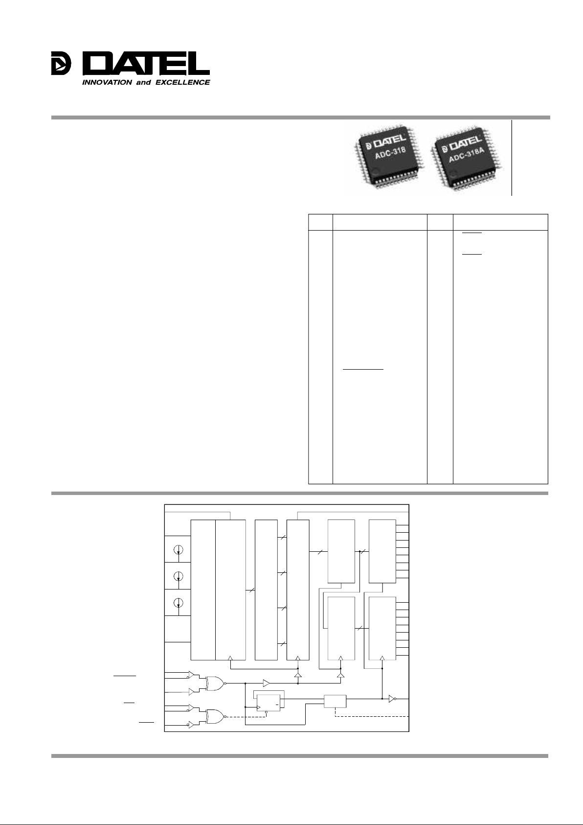
Figure 1. ADC-318/318A Functional Block Diagram
1 –DVs (Digital) 48 RSET ECL/PECL
2 REF. BOTTOM (V
RB) 47 RSET ECL/PECL
3 ANALOG GROUND 46 RSET TTL
4 REF. MID POINT (V
RM1) 45 SELECT
5 +AV
S (Analog) 44 INV
6 ANALOG IN (V
IN) 43 TTL CLOCK OUT
7 REF. MID POINT (V
RM2) 42 +DVS2 (Digital)
8 +AV
S (Analog) 41 DIGITAL GROUND 2
9 REF. MID POINT (V
RM3) 40 A BIT 1 (MSB)
10 ANALOG GROUND 39 A BIT 2
11 REF. TOP (V
RT) 38 A BIT 3
12 DIGITAL GROUND 3 37 A BIT 4
13 A/D CLOCK ECL/PECL 36 A BIT 5
14 A/D CLOCK ECL/PECL 35 A BIT 6
15 A/D CLOCK TTL 34 A BIT 7
16 NO CONNECTION 33 A BIT 8 (LSB)
17 NO CONNECTION 32 DIGITAL GROUND 2
18 NO CONNECTION 31 +DV
S2 (Digital)
19 +DV
S2 (Digital) 30 +DVS1 (Digital)
20 DIGITAL GROUND 2 29 DIGITAL GROUND 1
21 B BIT 8 (LSB) 28 B BIT 1 (MSB)
22 B BIT 7 27 B BIT 2
23 B BIT 6 26 B BIT 3
24 B BIT 5 25 B BIT 4
INPUT/OUTPUT CONNECTIONS
PIN FUNCTION PIN FUNCTION
256
ENCODER
COMPARATOR
SELECT
6
11
9
7
4
2
13
14
15
48
47
46
V
IN
V
RT
V
RM3
VRM2
VRM1
V
RB
A/D CLOCK ECL/PECL
A/D CLOCK TTL
RSET ECL/PECL
RSET TTL
RESISTOR
MATRIX
6-BIT LATCH
AND ENCODER
6
6
6
6
DELAY
D Q
Q
8 8
6
A
LATCH
B
LATCH
A
TTL
OUTPUT
B
TTL
OUTPUT
TTL
44 INV
33 BIT 8 (LSB)
34 BIT 7
35 BIT 6
36 BIT 5 A OUTPUT
37 BIT 4
38 BIT 3
39 BIT 2
40 BIT 1 (MSB)
21 BIT 8 (LSB)
22 BIT 7
23 BIT 6
24 BIT 5 B OUTPUT
25 BIT 4
26 BIT 3
27 BIT 2
28 BIT 1 (MSB)
43 CLOCK OUT
45 SELECT
A/D CLOCK ECL/PECL
RSET ECL/PECL
GENERAL DESCRIPTION
The ADC-318 and ADC-318A are 8 bit monolithic bipolar,
full flash A/D converters. Though they have high, 120MHz
(ADC-318) and 140MHz (ADC-318A), sampling rates, their
input logic level, including the start convert pulse, is TTL,
ECL and PECL compatible. Digital outputs are also TTL
compatible and allow a straight output or a programmable
1:2 de-multiplexed output.
The ADC-318 and ADC-318A feature ±1/2 LSB max.
integral and differential non-linearity, +5V single or ±5V dual
power supply operation, a low 960mW maximum power
dissipation, 150MHz wide analog input range and excellent
temperature coefficient in a small 48 pin QFP package. The
start convert pulse can have a 50% duty cycle.
The ADC-318 and ADC-318A offer low cost, easy to use
functionality for design engineers.

ADC-318, ADC-318A
2
® ®
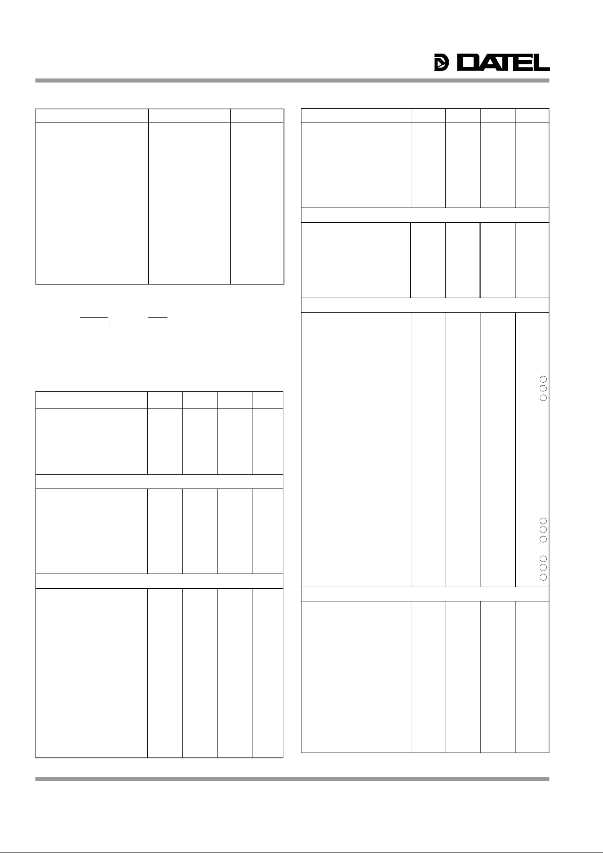
DIGITAL INPUTS MIN. TYP. MAX. UNITS
A/D Clock Pulse Width (T
PW1)
ADC-318 3.2 — — ns
ADC-318A 3.0 — — ns
A/D Clock Pulse Width (T
PW0)
ADC-318 3.2 — — ns
ADC-318A 3.0 — — ns
RSET Setup Time (T
rs) 3.5 — — ns
RSET Hold Time (T
rh) 0 — — ns
DIGITAL OUTPUTS
Output Voltage "1" (@–2mA) 2.4 — — Volts
Output Voltage "0" (@1mA) — — +0.5 Volts
Output Rise Time (T
r) ➃ — 2 — ns
Output Fall Time (T
f) ➃ — 2 — ns
Output Delay (T
do1) ➄ 1/Fc 1/Fc+1 1/Fc+2 ns
Output Delay (T
do2) ➅ 6.5 8 10 ns
Clockout Output Delay (T
dclk) ➆ 4.5 7 8 ns
PERFORMANCE
Resolution 8 — — Bit
Conversion Rate (f
S)
Straight Mode
ADC-318 100 — — MHz
ADC-318A 100 — — MHz
De-multiplexed Mode
ADC-318 100 — — MHz
ADC-318A 100 — — MHz
Sampling Delay (T
dS) 3 4.5 6 ns
Aperture Jitter (Taj) — 10 — ps
Integral Linearity Error — — ±0.5 LSB
Diff. Linearity Error — — ±0.5 LSB
S/N Ratio ➇
ADC-318
(@f
IN = 1kHz) — 46 — dB
(@f
IN = 29.999MHz) — 40 — dB
ADC-318A
(@f
IN = 1kHz) — 46 — dB
(@f
IN = 34.999MHz) — 40 — dB
Error Rate
ADC-318
(@f
IN = 1kHz) ➈ — — 10
-12
TPS
(@f
IN = 29.999MHz) — — 10
-9
TPS
(@fIN = 24.999MHz)➉ — — 10
-9
TPS
ADC-318A
(@f
IN = 1kHz) ➈ — — 10
-12
TPS
(@f
IN = 34.999MHz) — — 10
-9
TPS
(@fIN = 24.999MHz)➉ — — 10
-9
TPS
POWER REQUIREMENTS
Supply Voltage
One Power Supply
(+AV
S, +DVS 1,2) +4.75 +5.0 +5.25 Volts
One Power Supply (DGND3) +4.75 +5.0 +5.25 Volts
One Power Supply (–DV
S) –0.05 0 +0.05 Volts
Two Power Supply
(+AV
S, +DVS 1,2) +4.75 +5.0 +5.25 Volts
Two Power Supply (DGND3) –0.05 0 +0.05 Volts
Two Power Supply (–DV
S) –5.5 –5.0 –4.75 Volts
ADC-318
Supply Current (+I
S) 125 145 185 mA
Supply Current (–I
S) 0.4 0.6 0.8 mA
ADC-318A
Supply Current (+z
S) 110 150 185 mA
Supply Current (–z
S) 0.4 0.6 0.8 mA
ANALOG INPUTS MIN. TYP. MAX. UNITS
Input Voltage — +2 to +4 — Volts
Input Resistance 4 — 50 kΩ
Input Current 0 — 500 µA
Input Capacitance ➀ — 21 — pF
Input Bandwidth
V
IN = 2Vp-p, –3dB 150 — — MHz
REFERENCE INPUTS
Reference Voltage
VRT +2.9 — +4.1 Volts
VRB +1.4 — +2.6 Volts
VRT–VRB 1.5 — 2.1 Volts
Reference Resistance 75 115 155 Ω
Reference Current 9.7 17.4 28 mA
V
RT Offset Voltage 2 — 15 mV
V
RB Offset Voltage 2 — 10 mV
DIGITAL INPUTS
ECL, PECL
Input Voltage "1"
DGND3–1.05 — DGND3–0.5 Volts
Input Voltage "0"
DGND3–3.2 — DGND3–1.4 Volts
Threshold Voltage —
DGND3–1.2 — Volts
Input Current "1" ➁ –50 — +50 µA
Input Current "0" ➁ –75 — 0 µA
Voltage Difference 0.4 0.8 — Volts
TTL
Input Voltage "1" +2.0 — — Volts
Input Voltage "0" — — +0.8 Volts
Threshold Voltage — +1.5 — Volts
Input Current "1" ➂ –50 — 0 µA
Input Current "0" ➂ –500 — 0 µA
Select
Input Voltage "1" — +DVS1 —
Output Voltage "0" — +DGND1 —
Input Capacitance — — 5 pF
PARAMETERS LIMITS UNITS
Supply Voltage (+AVS, +DVS, 1,2) –0.5 to +7.0 Volts
Supply Voltage (AGND, DGND 1, 2) –0.5 to +7.0 Volts
Supply Voltage (DGND 3) –0.5 to +7.0 Volts
Supply Voltage (–DVS) ➀ –0.5 to +7.0 Volts
Supply Voltage (–DVS) ➁ –7.0 to +0.5 Volts
Reference Voltage (VRT) +2.7 to +AVS Volts
Reference Voltage (VRB) VIN –2.7 to +AVS
Reference Voltage (VRT–VRB1) 2.5 Volts
Input Voltage, analog (VIN) VRT –2.7 to +AVS Volts
Input Voltage, digital
ECL –DVS to +0.5 Volts
PECL –0.5 to DGND3 Volts
TTL –0.5 to +DVS1 Volts
Diff. Voltage between Pin ➂ 2.7 Volts
Power Dissipation, max. ➃ 2 W
ABSOLUTE MAXIMUM RATINGS
Footnote:
➀ Single Supply
➁ Dual Supply
➂ A/D Clock–A/D Clock and RESET–RESET of ECL/PECL logic inputs.
➃ With ADC-318 mounted on a 50x50mm glass fiber base
epoxy board, 1.6mm thick.
FUNCTIONAL SPECIFICATIONS
(Typical at TA = 25°C, VRT = +4V, VRB = +2V, DGND3 = +DVS1= +DVS2 = +AVS =
+5V, –DVS = 0V, PECL Logic, unless otherwise specified.)
13
13
13
11
11
11
11
11
11

ADC-318, ADC-318A
3
® ®
318A requires that the characteristic impedance of all input/
output logic and analog input lines be properly matched.
2. Power supply lines and grounding may effect the performance of the ADC-318 and ADC-318A. Separate and
substantial AGND and DGND ground planes are required.
These grounds have to be connected to one earth point
underneath the device. There are three digital grounds,
DGND1 (pin 29), DGND2 (pins 20, 32, 41) and DGND3 (pin
12). These DGND 's are separated internally. DGND1 and
DGND2 are always connected externally but DGND3 shall
be connected differently depending on whether the single or
dual power supply mode is used, as explained later.
The ADC-318 and ADC-318A have separate +AVs and
+DVs pins. It is recommended that both +AVs and +DVs be
powered from a single source. Other external digital circuits
must be powered with a separate +DVs. Layouts of +AVs
and +DVs lines must be separated like the GND lines to
avoid mutual interference and are connected to a point
through an LC filter. There are two digital supplies +DVs1
(pin 30) and +DVs2 (pins 19, 31, 42). These are also
separated internally. These must be tied together outside
while in use. Bypassing all power lines with a 0.1uF ceramic
chip capacitor and the use of multilayered PC boards is
recommended.
3. The analog input terminal (pin 6) has 21pF of input capacitance. The input signal has to be given via a buffer amplifier
which has enough driving power. Make lead wires as short
as possible and use chip resistors and capacitors to avoid
parasitic capacitance and inductance.
4. The use of a buffer amplifier and bypass capacitors is also
recommended on the reference input terminals VRT (pin 11)
and VRB (pin 2). The analog input range is determined by
POWER REQUIREMENTS (cont.)
Power Dissipation
ADC-318 680 780 980 mW
ADC-318A 570 790 960 mW
PARAMETERS
Operating Temp. Range, Case
ADC-318, 318A –20 — +75 °C
Thermal Impedance
θja — 62.5 — °C/Watt
Storage Temperature Range –65 — +150 °C
Package Type 48-pin, plastic QFP
Weight 0.25 ounces (0.7 grams)
Footnotes:
➀ VIN = +3V +0.07Vrms
➁ VIH = DGND3–0.8V
VIL = DGND3–1.6V
➂ VIH = 3.5V
VIL = 0.2V
➃ TTL, 0.8 to 2.0V, CL = 5pF
➄ DMUX Mode, CL = 5pF; FC = Clock
frequency
➅ Straight Mode, CL = 5pF
➆ CL = 5pF
➇ VIN = FS, DMUX mode
➈ VIN = FS, DMUX mode, Error >16LSB
➉ VIN = FS, Straight mode, Error >16LSB
"Times Per Sample"
Mounted on 50x50mm, 1.6mm thick
glass fiber base epoxy board
TECHNICAL NOTES
1. The ADC-318 and ADC-318A are ultra high speed full flash
A/D converters that have 120MHz and 140MHz sampling
rates respectively. The ADC-318 and ADC-318A are fully
interchangeable products with the exception of their
sampling rates. Their inputs are TTL, ECL and PECL
compatible and their outputs are TTL compatible. Obtaining
fully specified performance from the ADC-318 and ADC-
12
11
12
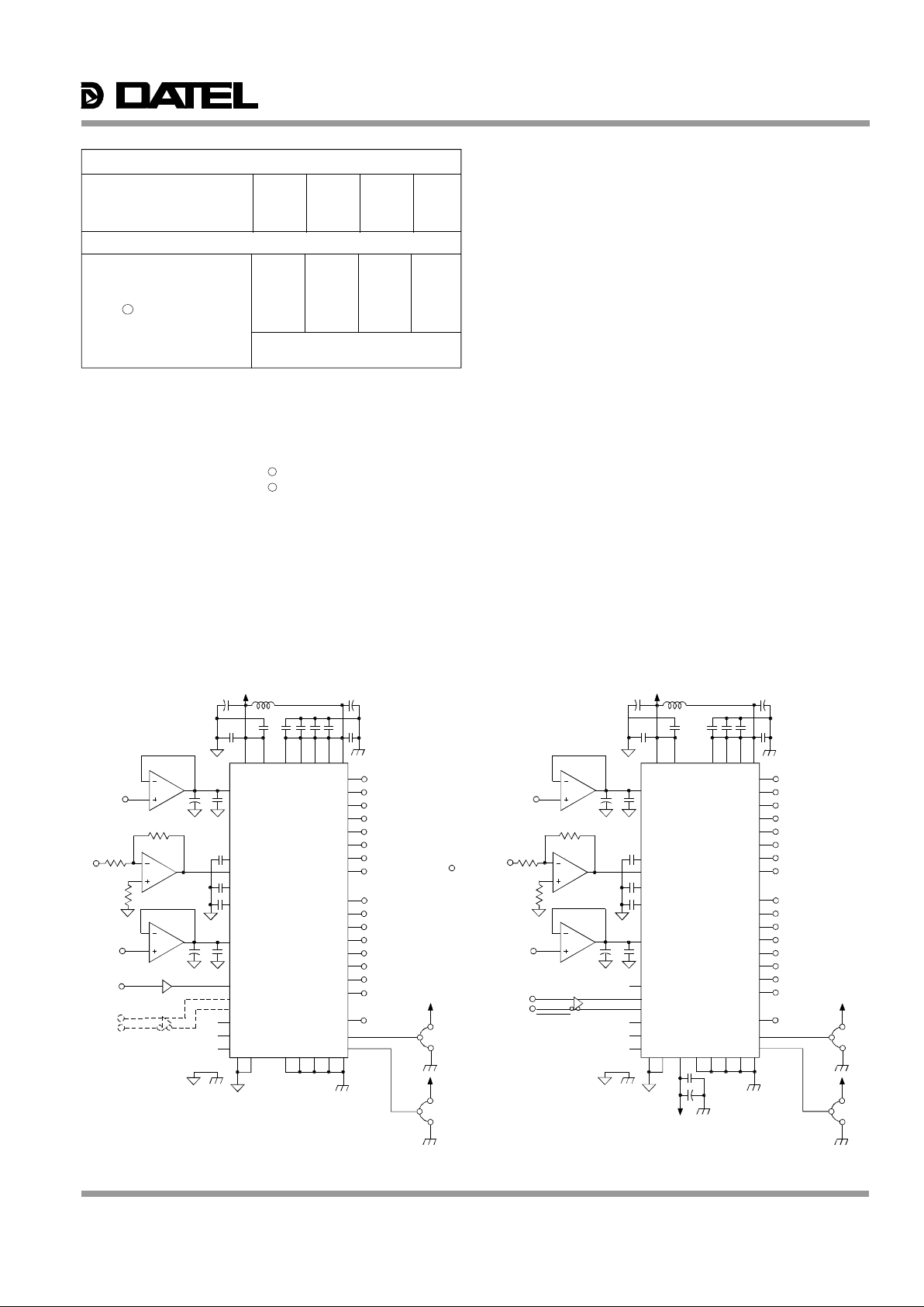
Figure 2-1: One Power Supply Operation (TTL, PECL)
Figure 2-2: Two Power Supply Operation (ECL)
Note: All capacitors not otherwise designated are 0.1µF
+ +
+
+
5V(A)
10µF
10µH 5V(D)
10µF
85 19 30 31 42
10µF
2
V
RB
+2V
ANALOG IN
+2V to +4V
4
6
7
9
11
VRT
+4V
10µF
A/D CLOCK
15
13
14
48
47
46
3 10
20 29 32
41
45
44
43
TTL
CLOCK OUT
5V(D)
28 B BIT 1
27 B BIT 2
26 B BIT 3
25 B BIT 4
24 B BIT 5
23 B BIT 6
22 B BIT 7
21 B BIT 8
LSB
MSB
40 A BIT 1
39 A BIT 2
38 A BIT 3
37 A BIT 4
36 A BIT 5
35 A BIT 6
34 A BIT 7
33 A BIT 8
LSB
MSB
ADC-318
12
1
TTL
PECL
ADC-318A
5V(D)
+ +
+
+
+
5V(A)
10µF
10µH 5V(D)
10µF
85 19 30 31 42
10µF
2
V
RB
+2V
ANALOG IN
+2V to +4V 4
6
7
9
11
VRT
+4V
10µF
ECL
A/D CLOCK
A/D CLOCK
15
13
14
48
47
46
3 10
1 12
20 29 32
41
10µF
5V(D)
45
44
43
TTL
CLOCK OUT
28 B BIT 1
27 B BIT 2
26 B BIT 3
25 B BIT 4
24 B BIT 5
23 B BIT 6
22 B BIT 7
21 B BIT 8
LSB
MSB
40 A BIT 1
39 A BIT 2
38 A BIT 3
37 A BIT 4
36 A BIT 5
35 A BIT 6
34 A BIT 7
33 A BIT 8
LSB
MSB
ADC-318
ADC-318A
5V(D)
5V(D)
 Loading...