

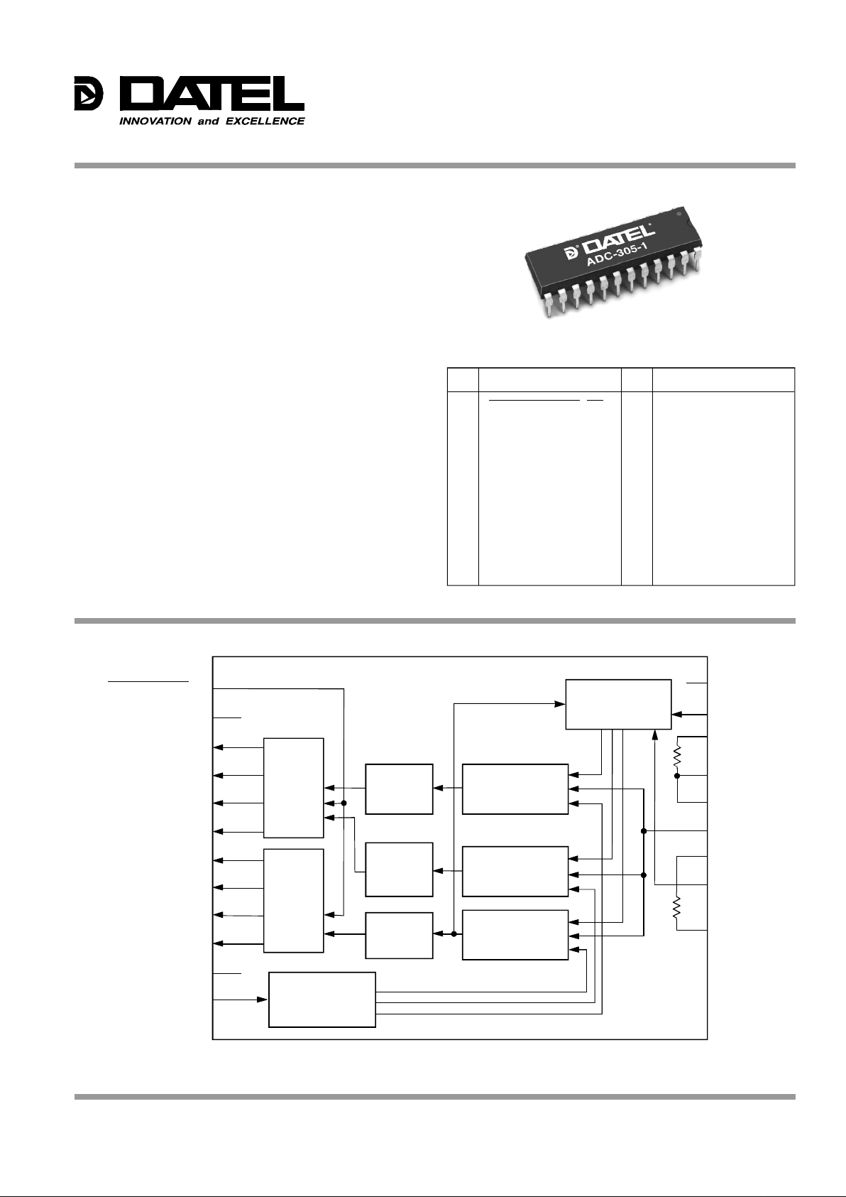
DATEL ADC-305-3, ADC-305-1 Datasheet
PIN FUNCTION PIN FUNCTION
1 OUTPUT ENABLE (OE) 24 DGND
2 DGND 23 REF. BOTTOM (V
RB)
3 BIT 8 (LSB) 22 SELF BIAS 1 (V
RBS)
4 BIT 7 21 AGND
5 BIT 6 20 AGND
6 BIT 5 19 ANALOG INPUT (V
IN)
7 BIT 4 18 +AV
S (+5V)
8 BIT 3 17 REFERENCE TOP (V
R
T)
9 BIT 2 16 SELF BIAS 2 (V
RTS)
10 BIT 1 (MSB) 15 +AV
S (+5V)
11 +DV
S (+5V) 14 +AVS (+5V)
12 CLOCK INPUT (A/D CLK) 13 +DV
S (+5V)
FEATURES
• 8-bit resolution, 20MHz min. sampling rate
• ±½LSB max. differential nonlinearity error
• 18MHz input signal bandwidth
• Subranging, S&H enclosed
• +5V single power, low 85mW max. dissipation
• CMOS compatible logic input
• 3-State TTL compatible output
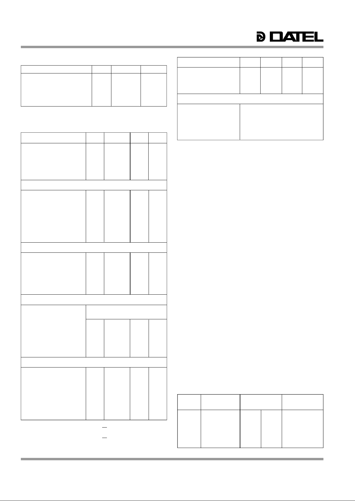
Figure 1. Functional Block Diagram
INPUT/OUTPUT CONNECTIONS
ADC-305
8-Bit, 20MHz
CMOS A/D Converters
Both the ADC-305-1 and the ADC-305-3 have the same pin assignment.
GENERAL DESCRIPTION
DATEL's ADC-305 is an 8-bit, 20MHz sampling, CMOS,
subranging (two-pass) A/D converter. It processes signals at
speeds comparable to a full flash converter by using a subranging conversion technique with multiple comparator blocks,
each containing a sample and hold amplifier.
The ADC-305 features CMOS low power dissipation (60mW
typical) and a wide 18MHz (–1dB) input signal bandwidth.
The ADC-305-1 is packaged in 400 mil 24-pin DIP and the
ADC-305-3 in 300 mil 24-pin SOP.
Other features are CMOS compatible input logic, 3-state TTL
compatible output logic, +5V single power operation, self bias
mode and low cost.
DATEL, Inc., Mansfield, MA 02048-1151 (USA) • Tel: (508)339-3000, (800)233-2765 Fax: (508)339-6356 • Email: sales@datel.com • Internet www.datel.com
UPPER
ENCODER
(4 BIT)
24 DGND
OUTPUT ENABLE 1
A/D CLK 12
BIT 8 (LSB) 3
BIT 1 (MSB) 10
BIT 7 4
23 V
RB
21 A
GND
20 A
GND
19 VIN
15 +AV
S
14 +AVS
13 +DV
S
18 +AVS
17 VRT
22 V
RBS
16 V
RTS
REFERENCE
VOLTAGE
B BLOCK
COMPARATORS
WITH S/H (4 BIT)
UPPER
COMPARATORS
WITH S/H (4 BIT)
LOWER
ENCODER
(4 BIT)
LOWER
ENCODER
(4 BIT)
CLOCK
GENERATOR
UPPER
DATA
LATCHES
LOWER
DATA
LATCHES
A BLOCK
COMPARATORS
WITH S/H (4 BIT)
DGND 2
+DV
S 11
BIT 6 5
BIT 5 6
BIT 4 7
BIT 3 8
BIT 2 9
® ®
ADC-305
® ®
TECHNICAL NOTES
1. The ADC-305 has separate +AVS and +DVS pins. It is
recommended that both +AV
S and +DVS be powered from a
single supply since a time lag between start up of separate
supplies could induce latch up. Other external logic circuits
must be powered from a separate digital supply. +DV
S (pins
11 and 13) and +AVs (pins 14, 15 and 18) should be tied
together externally. DGND (pins 2 and 24) and AGND (pins
20 and 21) should also be tied together externally. Power
supply grounds must be connected at one point to the
ground plane directly beneath the device. Digital returns
should not flow through analog grounds.
2. Bypass all power lines to ground with a 0.1µF ceramic chip
capacitor in parallel with a 47µF electrolytic capacitor.
Locate the bypass capacitor as close to the unit as
possible.
3. Even though the analog input capacitance is a low 15pF, it
is recommended that high frequency input be provided via
a high speed buffer amplifier. A parasitic oscillation may be
generated when a high speed amplifier is used. A 75 ohm
resister inserted between the output of an amplifier and the
analog input of the ADC-305 will improve the situation. A
resistor larger than 100 ohms may degrade linearity.
4. The input voltage range is determined by voltages applied
to V
RB (Reference Bottom) and VRT (Reference Top). Keep
to the following equations;
0V≤V
RB≤VRT≤2.8V
1.8V≤V
RT–VRB≤2.8V
The analog input range is normally 2Vp-p.
Self Bias Mode
a. Tie V
RB to VRBS, and tie VRT to VRTS respectively. The analog
input range in this case is +0.64V to +2.73V nominal.
b. Tie V
RB to AGND, and tie VRT to VRTS respectively. The
analog input voltage range is 0 to +2.39V in this case.
FUNCTIONAL SPECIFICATIONS
(Specification are typical at TA = +25°C, +VRT = +2.5V, VRB = +0.5V, +AVS = +DVS =
+5v, f
S
= 20MHz sampling unless otherwise specified.)
ANALOG INPUTS MIN. TYP. MAX. UNITS
Input Voltage Range (V
IN) ➀ — +0.5 to +2.5 — Volts
Input Capacitance — 11 — pF
(V
IN = 1.5Vdc+0.07VRMS)
Input Impedance — 12.5 — kΩ
Input Signal Bandwidth — 18 — MHz
(V
IN-2Vp-p, –1dB)
REFERENCE INPUTS
Ref. Resitance V
RT to VRB 230 300 450 Ω
Ref. Current 4.5 6.6 8.7 mA
Ref. Voltage ➀ V
RT +1.8 — +2.8 Volts
V
RB 0 — VRT Volts
Offset Voltage V
RT –10 –35 –60 mV
V
RB 0 +15 +45 mV
Self Bias I ➀ ➁V
RBS +0.6 +0.64 +0.68 Volts
V
RTS-VRBS +1.96 +2.09 +2.21 Volts
Self Bias II ➀ ➂V
RTS +2.25 +2.39 +2.53 Volts
DIGITAL INPUTS
Input Voltage (CMOS)
Logic Levels (V
IH) "1" +4 — — Volts
Logic Level (V
IL) "0" — — +1 Volts
Input Current (@V
IH=+DVS)"1" — — 5 µA
(@V
IL=0) "0" — — 5 µA
Clock Pulse Width T
PW1 25 — — ns
(A/D CLK) T
PW0 25 — — ns
DIGITAL OUTPUTS
Output Data 8-bit Binary Parallel
Output Voltage 3-State TTL compatible
Output Current ➃
Logic Level "1" –1.1 — — mA
Logic Level "0" +3.7 — — mA
Output Current ➄
Logic Level "1" — — 16 µA
Logic Level "0" — — 16 µA
Output Data Delay, Td — 18 30 ns
PERFORMANCE
Resolution 8 — — Bit
Maximum Sampling Rate 20 — — MHz
Minimum Sampling Rate — — 0.5 MHz
Aperature Delay, T
A — 4 — ns
Aperature Jitter — 30 — ps
Differential Linearity Error — ±0.3 ±0.5 LSB
Integral Linearity Error — +0.5 +1.3 LSB
Differential Gain Error ➅ — 1 — %
Differential Phase Error ➅ — 0.5 — deg
POWER REQUIREMENTS MIN. TYP. MAX. UNITS
Power Supply (+AV
S, +DVS) +4.75 +5.0 +5.25 Volts
I A GND - D GND I — — 100 mV
Power Supply Current — 12 17 mA
Power Dissipation — 60 85 mW
PHYSICAL/ENVIRONMENTAL
Operating Temp. Range –40 to +85°C
Storage Temp. Range –55 to +150°C
Package Type ADC-305-1 24-pin Plastic DIP
ADC-305-3 24-pin Plastic SOP
Weight ADC-305-1 2.0 grams
ADC-305-3 0.3 grams
Footnotes:
➀ See Technical Note 4
➁ Short V
RB (pin 23) to VRBS (pin 22).
Short V
RT (pin 17) to VRTS (pin 16).
➂ Short V
RB (pin 23) to A GND.
Short V
RT (pin 17) to VRTS (pin 16).
2
➃ OE=OV, VOH=+DVS–0.5V,
V
OL=+0.4V
➄ OE=+DV
S, VOH=+DVS, VOL=0V
➅ NTSC 40IRE mode ramp, 14.3MHz
sampling
Table 1. Digital Output Coding
PARAMETERS MIN MAX UNITS
Power Supply Voltage (+AV
S, +DVS) –0.5 +7 Volts
Analog Input Voltage (V
IN) –0.5 +AVS +0.5 Volts
Reference Input Voltage (V
RT, VRB) –0.5 +AVS +0.5 Volts
Digital Input Voltage (V
IH, VIL) –0.5 +DVS +0.5 Volts
Digital Output Voltage (V
OH, VOL) –0.5 +DVS +0.5 Volts
ABSOLUTE MAXIMUM RATINGS (TA = 25°C)
STEP DATA BITS OUT
VIN CODE DEC HEX MSB LSB
O
V Zero 0 00 0 0 0 0 0 0 0 0
+0.9922V +1/2FS –1LSB 127 7F 0 1 1 1 1 1 1 1
+1.000V +1/2FS 128 80 1 0 0 0 0 0 0 0
+1.9922V +FS 255 FF 1 1 1 1 1 1 1 1
➔➔➔➔➔➔➔
➔➔➔
 Loading...