

DATEL ADC-304-3, ADC-304 Datasheet
INPUT/OUTPUT CONNECTIONS
PLASTIC DIP PACKAGE
PIN FUNCTION PIN FUNCTION
1 BIT 1 (MSB) 28 MINV
2 BIT 2 27 V
M
3 BIT 3 26 V
B
4 BIT 4 25 ANALOG GND
5 DIGITAL GND 24 NO CONNECT
6 +5V POWER 23 ANALOG INPUT
7 –5.2V POWER 22 NO CONNECT
8 –5.2V POWER 21 ANALOG INPUT
9 –5.2V POWER 20 NO CONNECT
10 +5V POWER 19 ANALOG GND
11 DIGITAL GND 18 V
T
12 LINV 17 CLOCK INPUT
13 BIT 5 16 BIT 8 (LSB)
14 BIT 6 15 BIT 7
FEATURES
• 8-bit resolution
• 20MHz conversion rate
• ±1/2LSB maximum nonlinearity
• 8MHz input bandwidth
• Low power consumption, 375mW
• TTL compatible
• Single or dual supply operation
GENERAL DESCRIPTION
Datel’s ADC-304 is an 8-bit, 20MHz analog-to-digital flash
converter. The ADC-304 offers many performance features not
obtainable from other flash A/D’s.
Key reatures include a low power dissipation of 375mW and
TTL-compatible outputs. A wide analog input bandwidth of
8MHz (–3dB) allows operation without the need of a samplehold. Also, single +5V supply operation is obtainable with an
input range of +3 to +5V, eliminating the need for an additional
power supply. A 0 to –2V input range is available with ±5V
supply operation.
Another novel feature of the ADC-304 is its user-selectable
output coding. The MINV and LINV pins allow selection of
binary, complementary binary, and if external offset circuitry is
used for bipolar inputs, offset binary, two’s complement and
complementary two’s complement coding.
The ADC-304 is supplied in a 28-pin plastic DIP or a 28-pin
plastic SOP package. Operating temperature range is –20 to
+75°C. Storage temperature range is –55 to +150°C.
INPUT/OUTPUT CONNECTIONS
PLASTIC SOP PACKAGE
PIN FUNCTION PIN FUNCTION
1 ANALOG INPUT 28 ANALOG INPUT
2 V
B
SENSE 27 VT SENSE
3 ANALOG GND 26 ANALOG GND
4 V
B
25 V
T
5 V
M
24 CLOCK INPUT
6 NO CONNECT 23 BIT 8 (LSB)
7 MINV 22 BIT 7
8 BIT 1 (MSB) 21 BIT 6
9 BIT 2 20 BIT 5
10 BIT 3 19 LINV
11 BIT 4 18 DIGITAL GND
12 DIGITAL GND 17 +5V POWER
13 +5V POWER 16 OVERRANGE
14 –5.2V POWER 15 –5.2V POWER
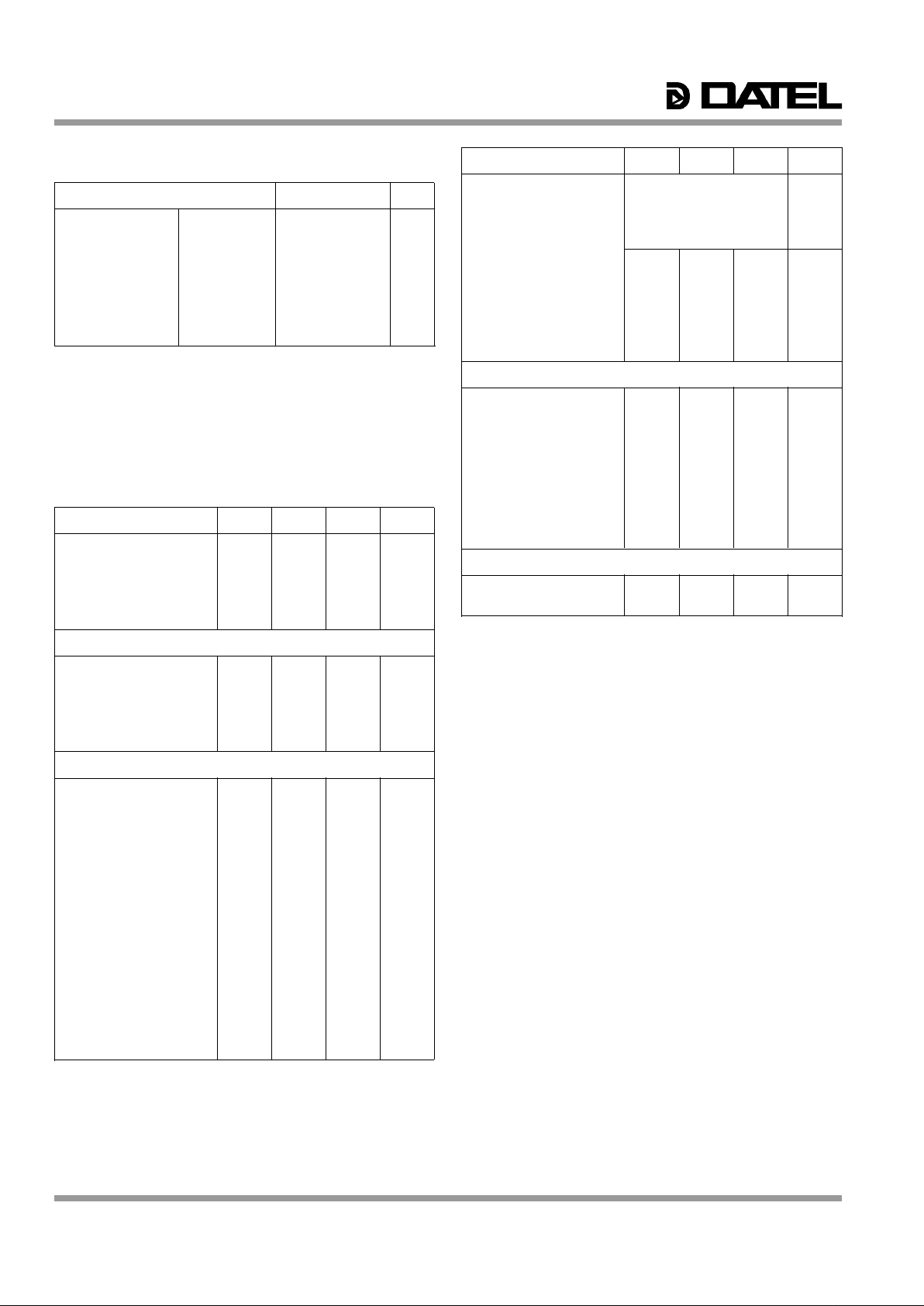
Figure 1. ADC-304 Functional Block Diagram
INNOVATION and EX C ELL E N C E
® ®
BIT 1 (MSB)
BIT 2
BIT 3
BIT 4
OVERRANGE ➀
CLOCK
INPUT
BIT 8 (LSB)
LINV
BIT 7
BIT 6
BIT 5
ANALOG
INPUT
VB
VB SENSE ➀
R/2
R/2
R/2
R
R
R
R
7
6
6
6
2
5
6
-
T
O
-
2
4
B
I
T
E
N
C
O
D
E
R
2
4
-
T
O
-
8
B
I
T
E
N
C
O
D
E
R
L
A
T
C
H
O
U
T
P
U
T
B
U
F
F
E
R
6
COMPARATOR
LATCH
1
256
129
128
3
2
1
VM
VT SENSE ➀
MINV
➀
THESE PINS ARE AVAILABLE ON SOP PACKAGE ONLY
V
T
ANALOG
INPUT
ADC-304
8-Bit, 20MHz, Low-Power
Flash A/D Converters
DATEL, Inc., 11 Cabot Boulevard, Mansfield, MA 02048-1151 (U.S.A.) • Tel: (508) 339-3000 Fax: (508) 339-6356 • For immediate assistance (800) 233-2765
® ®
ADC-304
FUNCTIONAL SPECIFICATIONS
Unless otherwise noted, the following specifications apply to the ADC-304 when used
either with a single or dual power source. The test conditions are:
For single power supply operation: For dual power supply operation:
+V
S
= +5V, DIG GND = 0V +VS = +5V, DIG GND = 0V
–V
S
= 0V, VT = +5V –VS = –5.2V, VT = 0V,
V
B
= +3V, TA = +25°C VB = –2V, TA = +25°C
ANA GND = +5V, f
s = 20MHz ANA GND = 0V, fs = 20MHz
ANALOG INPUTS MIN. TYP. MAX. UNITS
Input Range V
B
V
T
Volts
Input Capacitance — 30 35 pF
Input Bias Current 15 50 100 µA
Offset Voltage
V
T
–8 –13 –19 mV
V
B
0 +5 +11 mV
DIGITAL INPUTS
Logic Levels
Logic “1” +2.0 — — Volts
Logic “0” — — +0.8 Volts
Logic Input Currents
Logic “1” — –100 –150 µA
Logic “0” –0.1 –0.32 –0.5 mA
PERFORMANCE
Conversion Rate ➀ 20 — — MHz
Integral Nonlinearity — — ±1/2 LSB
Differential Nonlinearity — — ±1/2 LSB
Differential Gain Error ➁ — — 1.5 %
Differential Phase Error ➁ — — 0.5 degrees
Aperture Delay Ta 5 7 9 ns
Aperture Uncertainty — 30 — ps
Signal-to-Noise and Distortion
(V
in = full scale, fs = 20MHz)
f
in = 1MHz 47 dB
f
in = 5MHz 43 dB
f
in = 10MHz 35 dB
Clock Pulse Width
Tpw1 35 — — ns
Tpw0 10 — — ns
Reference Pin Current 11 15 18 mA
Reference Resistance (V
T
to VB) — 130 — Ohms
Reference Input (dual supply)
V
T
–0.1 0 +0.1 Volts
V
B
–1.8 –2.0 –2.2 Volts
Footnotes:
➀ f
in = 1kHz, ramp
➁ NTSC 40 IRE-modulated ramp, f
s = 14.3MHz
ABSOLUTE MAXIMUM RATINGS
PARAMETERS LIMITS UNITS
Supply Voltages +V
S
to GND 0 to +6 Volts
–V
S
to GND 0 to –6 Volts
Input Voltage (Analog) Vin –V
S
to (ANA GND + 0.3) Volts
(dual power supply)
Input Voltage (Reference) V
T
, VB, V
M
–VS to (ANA GND + 0.3) Volts
(dual power supply)
❘ V
T
– VB ❘ 2.5 Volts
Input Current I
M
–3.0 to +3.0 mA
Input Voltage (Digital) Digital Inputs –0.5 to +V
S
Volts
DIGITAL OUTPUTS MIN. TYP. MAX. UNITS
Resolution and Output Coding 8 bits
Straight binary
Complementary binary
Two’s complement
Complementary two’s complement
Logic Levels
Logic “1” +2.7 +3.4 — Volts
Logic “0” — — +0.5 Volts
Logic Loading “1” — –500 — µA
Logic Loading “0” — — +3 mA
Output Data Delay
TDLH 15 20 30 ns
TDHL 22 26 35 ns
POWER REQUIREMENTS
Single Power Supply
Supply Voltage = +V
S
+4.75 +5.0 +5.25 Volts
Supply Voltage = –V
S
— 0 — Volts
Supply Current = +I
S
+56 +71 +91 mA
Power Dissipation 280 355 455 mW
Dual Power Supply
Supply Voltage = +V
S
+4.75 +5.0 +5.25 Volts
Supply Voltage = –V
S
–4.75 –5.2 –5.5 Volts
Supply Current = +I
S
+7 +10 +14 mA
Supply Current = –I
S
–50 –62 –78 mA
Power Dissipation 295 375 476 mW
PHYSICAL/ENVIRONMENTAL
Operating Temperature –20 — +75 °C
Storage Temperature –55 — +150 °C
TECHNICAL NOTES
1. The two DIGITAL GND pins (pins 5 and 11 on the DIP, pins
12 and 18 on the SOP) are not connected to each other
internally and neither are the two +5V POWER pins (6 and
10 on the DIP, 13 and 17 on the SOP). All four pins must be
externally connected to the appropriate pcb patterns. Also,
the DIGITAL GND and ANALOG GND pins are not
connected to each other internally.
2. Layout of the analog and digital sections should be
separated to reduce interference from noise. To further
guard against unwanted noise, it is recommended to
bypass, as close as possible, the voltage supply pins to
their respective ground pins with 1µF tantalum and 0.01µF
ceramic disk capacitors in parallel.
3. The input capacitance of the analog input is much smaller
than that of a typical flash A/D converter. It is necessary to
use an amplifier with sufficient bandwidth and driving power.
The analog input pins are separated internally, so they
should be connected together externally. If the ADC-304 is
driven with a low output impedance amplifier, parasitic
oscillations may occur.
These parasitic oscillations can be prevented by introducing
a small resistance of 2 to 10Ω between the amplifier output
and the ADC-304’s A/D input. This resistance must have a
very low value of series inductance at high frequencies.
Note that each of the analog input pins is divided in this
manner with these resistances. Connect the driving amplifier
as close as possible to the A/D input of the ADC-304.
2
 Loading...