

FEATURES
• 8-Bit flash A/D converter
• 20MHz sampling rate
• Complete support circuitry
• Low power, 1.5W
• 7MHz full power bandwidth
• Sample-hold not required
• Three-state outputs
• MIL-STD-883 versions
GENERAL DESCRIPTION
The ADC-228 combines analog front-end circuitry and a flash
A/D converter to digitize high-speed analog signals at a rate of
20 million samples per second. The ADC-228 contains an
8-bit, 20MHz, flash A/D, a wideband analog input buffer, a
precision voltage reference, temperature compensation
circuitry, reference trims, and a three-state output buffer in a
24-pin package.
The ADC-228 offers significant savings by combining all of the
circuitry in a single package. Valuable board real estate is
saved, and design time and manufacturing costs are reduced.
The ADC-228 is housed in a 24-pin ceramic DDIP package
and is available in the commercial, 0 to +70°C, or military,
–55 to +125°C, temperature ranges. A MIL-STD-883 version
is also available. Operation is from ±15V and +5V power
supplies.
INNOVATION and EX C ELL E N C E
® ®
ADC-228
8-Bit, 20MHz, Complete
Flash A/D Converter
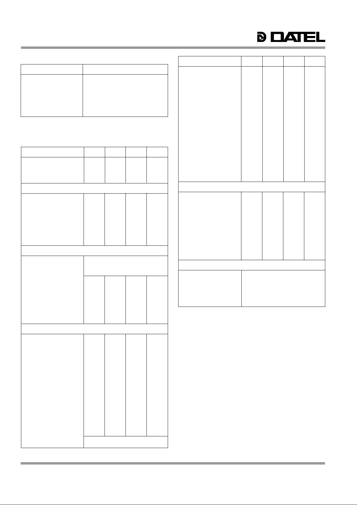
Figure 1. Functional Block Diagram
PIN FUNCTION PIN FUNCTION
1 +5V SUPPLY 24 BIT 8 (LSB)
2 GROUND 23 BIT 7
3 +5V REFERENCE OUT 22 BIT 6
4 GROUND 21 BIT 5
5 ANALOG INPUT 20 NO CONNECTION
6 GROUND 19 +15V SUPPLY
7 GROUND 18 CLOCK INPUT
8 NLINV 17 BIT 4
9 NMINV 16 BIT 3
10 –15V SUPPLY 15 BIT 2
11 CS1 14 BIT 1 (MSB)
12 CS1 13 NO CONNECTION
INPUT/OUTPUT CONNECTIONS
13 NO CONNECTION
20 NO CONNECTION
14 BIT 1 (MSB)
15 BIT 2
16 BIT 3
17 BIT 4
21 BIT 5
22 BIT 6
23 BIT 7
24 BIT 8 (LSB)
3 +5V REF. OUT
TRI-STATE
BUFFER
8-BIT
20MHz
FLASH
CONVERTER
LINEARIZATION
& TEMPERATURE
COMPENSATION
NETWORK
INPUT
BUFFER
CS1 11
CS1 12
NLINV 8
NMINV 9
CLOCK 18
ANALOG INPUT 5
+15V SUPPLY 19
GROUND 4
GROUND 7
GROUND 6
–15V SUPPLY 10
+5V SUPPLY 1
VOLTAGE
REFERENCE
NETWORK
GROUND 2
DATEL, Inc., 11 Cabot Boulevard, Mansfield, MA 02048-1151 (U.S.A.) • Tel: (508) 339-3000 Fax: (508) 339-6356 • For immediate assistance (800) 233-2765
ADC-228
® ®
FUNCTIONAL SPECIFICATIONS
(Apply over the operating temperature range with 20MHz clock and ±15V and +5V
power supply voltages, unless otherwise specified.)
ANALOG INPUTS MIN. TYP. MAX. UNITS
Single-Ended, Non-Isolated
Input Range, dc-20MHz 0 — +5.0 Volts
Input Resistance 2.45 2.5 2.55 kΩ
Input Capacitance — 5 10 pF
DIGITAL INPUTS
Logic Levels
Logic 1 +2.0 — — Volts
Logic 0 — — +0.8 Volts
Logic Loading
Logic 1 — — +160 µA
Logic 0 — — –0.5 mA
Clock Pulse Widths
"High" 25 — — ns
"Low" 19 — — ns
DIGITAL OUTPUTS
Coding
Resolution
Logic Levels
Logic 1 +2.4 — — Volts
Logic 0 — — +0.4 Volts
Logic Loading
Logic 1 — — –1 mA
Logic 0 — — +1 mA
Output Data Valid Delay
From Rising Edge — 30 40 ns
Output Hold Time 5 — — ns
PERFORMANCE
Sampling Rate ➀ 20 — — MHz
Differential Linearity ➁
Code Transitions — ±0.5 ±0.75 LSB
Code Centers — ±0.25 ±0.5 LSB
Integral Linearity, +25°C
End-point — ±0.5 ±0.75 LSB
Best-fit Line — ±0.35 ±0.5 LSB
Over Temperature End-point — — ±1 LSB
Best-fit Line — — ±1 LSB
Zero-Scale Offset
Code "0" to "1" Transition
+25°C — — ±0.5 LSB
–55 to +125°C — ±0.5 ±1.5 LSB
Gain error — ±0.5 ±1.5 LSB
Full Scale Absolute Accuracy — ±0.5 ±1.5 LSB
Differential Gain ➂ — 2 — %
Differential Phase ➂ — 1 — deg.
Aperture Delay — 8 — ns
Aperture Jitter — 50 — ps
No Missing Codes
Power Supply Rejection
DYNAMIC PERFORMANCE MIN. TYP. MAX. UNITS
Total Harm. Distortion, –0.5dB
DC to 2.5 MHz — –55 –53 dB
2.5 MHz to 5 MHz — –50 –48 dB
5 MHz to 10 MHz — –39 –36 dB
Signal-to-Noise Ratio
and Distortion, –0.5dB
DC to 2.5 MHz 44 49 — dB
2.5 MHz to 5 MHz 43 46 — dB
5 MHz to 10 MHz 35 38 — dB
Signal-to-Noise Ratio
w/o Distortion, –0.5 dB
DC to 2.5 MHz 45 48 — dB
2.5 MHz to 5 MHz 45 48 — dB
5 MHz to 10 MHz 42 45 — dB
Effective Bits, –0.5dB
DC to 2.5 MHz 7.1 7.75 — Bits
2.5 MHz to 5 MHz 6.9 7.4 — Bits
5 MHz to 10 MHz 5.6 6.1 — Bits
Input Bandwidth
Full Power 7 — — MHz
Small Signal (–20dB) 40 — — MHz
POWER SUPPLY
Power Supply Range
+15V Supply +11 +15 +15.75 Volts
–15V Supply –11 –15 –15.75 Volts
+5V Supply +4.75 +5 +5.25 Volts
Power Supply Current
+15V Supply — — +30 mA
–15V Supply — — –10 mA
+5V Supply — — +230 mA
Power Dissipation
±12V, +5V Nominal — 1.4 1.65 Watts
Over full supply range — 1.6 1.85 Watts
±15V, +5V Nominal — 1.5 1.75 Watts
PHYSICAL/ENVIRONMENTAL
Operating Temp. Range, Case
ADC-228MC 0 to +70°C
ADC-228MM, ADC-228/883 –55 to +125°C
Storage Temp. Range –65 to +150°C
Package Type 24-pin, ceramic DDIP
Weight 0.3 ounces (8.5 grams)
Footnotes:
➀ At full power input and chip selects enabled.
➁ See Technical Note 3.
➂ For 10-step, 40 IRE NTSC ramp test.
ABSOLUTE MAXIMUM RATINGS
PARAMETER LIMITS
Power Supply Voltage, Pin 1 –0.5 to +7V
Pin 19 –0.3 to +18V
Pin 10 +0.3 to –18V
Digital Inputs, Pins 8,9,11,12,18 –0.5 to +5.5V
Analog Input, Pin 5 –6 to +7.5V
Digital Outputs –0.5 to +5.5V (short circuit protected to ground)
Lead Temp. (10 seconds) +300°C
Over the operating temperature range
±0.02% FSR/%V
S
maximum
Straight bin., comp. bin., two's
comp.,
comp. two's comp.
8 bits
2

® ®
ADC-228
Table 2. ADC-228 Bipolar Output Coding
(Assumes analog input is externally offset)
TECHNICAL NOTES
1. Rated performance requires using good high-frequency
techniques. The analog and digital ground pins are
connected to each other internally. Avoid ground related
problems by connecting the grounds to one point, the
ground plane beneath the converter. Due to the inductance
and resistance of the power supply return paths, return the
analog and digital ground separately to the power supplies.
2. Bypass all the analog and digital supplies and the +5V
REFERENCE (pin 3) to ground with a 4.7µF, 25V tantalum
electrolytic capacitor in parallel with a 0.1µF ceramic
capacitor.
3. DATEL uses conservative definitions when specifying
integral linearity (end-point) and differential linearity (code
transition). The specifications using the less conservative
definitions have also been provided as a comparative
specification for products specified this way.
4. Single conversions (one-shot mode) would require another
clock edge to read out data. Users desiring to provide just
a single clock pulse could use the circuit shown in Figure 2
to obtain the data.
STRAIGHT BIN. COMP. BIN.
ANALOG NMINV = 0 NMINV = 1
INPUT CODE NLINV = 0 NLINV = 1
+4.96V +FS – 1 LSB 1111 1110 0000 0001
+3.75V + 3/4 FS 1100 0000 0011 1111
+2.50V + 1/2 FS 1000 0000 0111 1111
+1.25V + 1/4 FS 0100 0000 1011 1111
+0.02V + 1 LSB 0000 0001 1111 1110
0.00V ZERO 0000 0000 1111 1111
Table 1. ADC-228 Unipolar Output Coding
TWO’S COMP.
COMP. TWO’S COMP.
ANALOG NMINV = 1 NMINV = 0
INPUT CODE NLINV = 0 NLINV = 1
+2.480V +FS – 1 LSB 0111 1111 1000 0000
+1.250V +1/2 FS 0100 0000 1011 1111
+0.020V +1 LSB 0000 0001 1111 1110
+0.000V ZERO 0000 0000 1111 1111
–1.250V –1/2 FS 1100 0000 0011 1111
–2.480V –FS + 1 LSB 1000 0001 0111 1110
–2.500V –FS 1000 0000 0111 1111
CLOCK
OUT
74HC86
CLOCK
IN
100pF
50ns
40ns
25ns
PULSES
DATA N
SAMPLED
DATA N
VALID
250
Ω
Figure 3. ADC-228 Typical Connections
Figure 2. ADC-228 Single Clock Pulse
Circuit and Operation
24
23
B8 (LSB)
B7
9k
Ω
51
Ω
19
V
IN 5
+15V
*Optional
+
2, 4, 6, 7
+5V REFERENCE OUT
NO CONNECTION
3
13, 20
22
B6
21
B5
17
B4
16
B3
CS1 12
CLOCK 18
ANALOG
INPUT
15
B2
14
+
+
B1 (MSB)
4.7µF
NLINV 8
NMINV 9
0.1µF
101
–15V
+5V
CS1 11
* Use optional resistor only if
amp is not used to drive input.
ADC-228
+
0.1µF
0.1µF
0.1µF
4.7µF
4.7µF
4.7µF
EE
R = V /1.667mA
3

Table 3. Chip Select Truth Table
Figure 4. ADC-228 Timing Diagram
SAMPLE
N + 2
SAMPLE
N + 1
SAMPLE
N
OUTPUT
HOLD TIME
DATA
N – 1
DATA
N
DATA
N + 1
CLOCK
DIGITAL
OUTPUT
OUTPUT
DELAY
CS1 CS1
Pin 12 Pin 11 Bits 1-8
0 0 Three State Mode
0 1 Three State Mode
1 0 Data Outputted
1 1 Three State Mode
ADC-228
® ®
MECHANICAL DIMENSIONS INCHES (mm)
0.200 MAX.
(5.080)
0.235 MAX.
(5.969)
0.600 ±0.010
(15.240)
0.80 MAX.
(20.32)
0.100 TYP.
(2.540)
0.100
(2.540)
0.018 ±0.002
(0.457)
0.100
(2.540)
0.040
(1.016)
1.31 MAX.
(33.27)
1 12
13
24
1.100
(27.940)
0.190 MAX.
(4.826)
0.010
(0.254)
+0.002
–0.001
SEATING
PLANE
0.025
(0.635)
Dimension Tolerances
(unless otherwise indicated):
2 place decimal (.XX) ±0.010 (±0.254)
3 place decimal (.XXX) ±0.005 (±0.127)
Lead Material: Kovar alloy
Lead Finish: 50 microinches (minimum) gold plating
over 100 microinches (nominal) nickel plating
ORDERING INFORMATION
MODEL TEMPERATURE RANGE
ADC-228MC 0 to +70°C
ADC-228MM –55 to +125°C
ADC-228/883 –55 to +125°C
Receptacle for PC board mounting can be ordered through AMP Inc., part # 3-331272-8
(component lead socket), 24 required. Contact DATEL for 883 product specifications
INNOVATION and EX C ELL E N C E
® ®
DATEL makes no representation that the use of its products in the circuits described herein, or the use of other technical information contained herein, will not infringe upon existing or future patent rights. The descriptions contained herein
do not imply the granting of licenses to make, use, or sell equipment constructed in accordance therewith. Specifications are subject to change without notice. The DATEL logo is a registered DATEL, Inc. trademark.
DS-0211B 10/96
ISO 9001
ISO 9001
REGISTERED
DATEL, Inc. 11 Cabot Boulevard, Mansfield, MA 02048-1151
Tel: (508) 339-3000 (800) 233-2765 Fax: (508) 339-6356
Internet: www.datel.com E-mail:sales@datel.com
Data Sheet Fax Back: (508) 261-2857
DATEL (UK) LTD. Tadley, England Tel: (01256)-880444
DATEL S.A.R.L. Montigny Le Bretonneux, France Tel: 1-34-60-01-01
DATEL GmbH München, Germany Tel: 89-544334-0
DATEL KK Tokyo, Japan Tel: 3-3779-1031, Osaka Tel: 6-354-2025
 Loading...