

Datasheet ADC-207MM-QL, ADC-207MM, ADC-207MC, ADC-207LM-QL, ADC-207LM Datasheet (DATEL)
...Page 1
INNOVATION and EX C ELL E N C E
® ®
INPUT/OUTPUT
CONNECTIONS
DIP LCC
PINS FUNCTION PINS
1 CLOCK INPUT 1
2 DIGITAL GROUND 4
3 –REFERENCE 5
4 ANALOG INPUT 6
5 MIDPOINT 7
6 +REFERENCE 8
7 ANALOG GROUND 9
8 CS1 11
9 CS2 12
10 OVERFLOW 13
11 BIT 1 (MSB) 14
12 BIT 2 16
13 BIT 3 17
14 BIT 4 19
15 BIT 5 20
16 BIT 6 21
17 BIT 7 (LSB) 23
18 +5V
SUPPLY 24
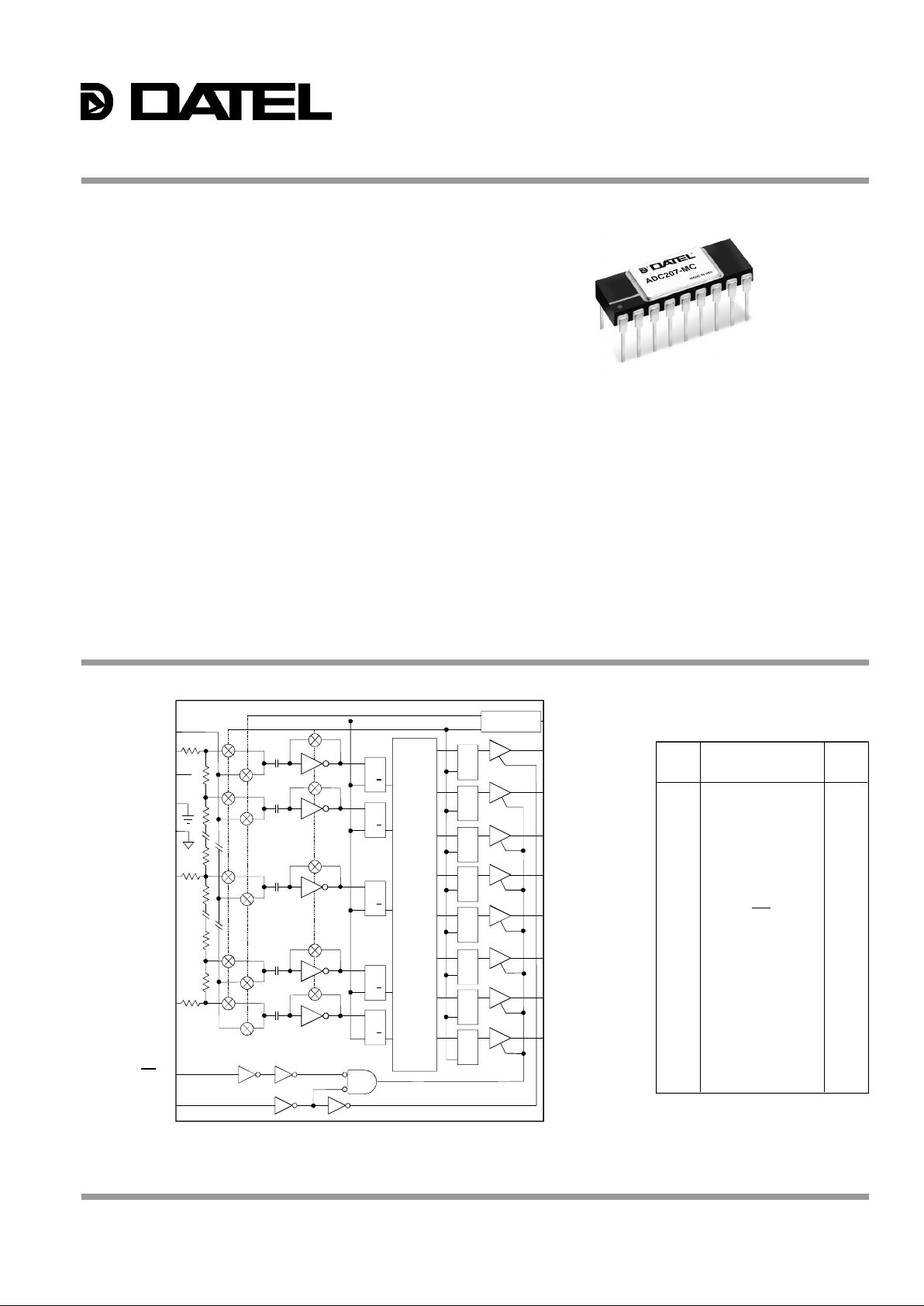
Figure 1. ADC-207 Functional Block Diagram (DIP Pinout)
FEATURES
• 7-bit flash A/D converter
• 20MHz sampling rate
• Low power (250mW)
• Single +5V supply
• 1.2 micron CMOS technology
• 7-bit latched 3-state output with overflow bit
• Surface-mount versions
• High-reliability version
• No missing codes
GENERAL DESCRIPTION
The ADC-207 is the industry’s first 7-bit flash converter using an
advanced high-speed VLSI 1.2 micron CMOS process. This
process offers some very distinctive advantages over other
processes, making the ADC-207 unique. The smaller
geometrics of the process achieve high speed, better linearity
and superior temperature performance.
Since the ADC-207 is a CMOS device, it also has very low
power consumption (250mW). The device draws power from
a single +5V supply and is conservatively rated for 20MHz
operation. The ADC-207 allows using sampling apertures as
small as 12ns, making it more closely approach an ideal
sampler. The small sampling apertures also let the device
operate at greater than 20MHz.
The ADC-207 has 128 comparators which are auto-balanced
on every conversion to cancel out any offsets due to
temperature and/or dynamic effects. The resistor ladder has a
midpoint tap for use with an external voltage source to improve
integral linearity beyond 7 bits. The ADC-207 also provides the
user with 3-state outputs for easy interfacing to other
components.
There are six models of the ADC-207 covering two operating
temperature ranges, 0 to +70°C and –55 to +125°C. Two highreliability "QL" models are also available.
D
G Q
D
G Q
D
G QDG Q
D
G QDG Q
D
G
Q
D
G
Q
DGQ
DGQ
D
G
Q
D
G
Q
D
G
Q
DGQ
ANALOG INPUT 4
+REFERENCE 6
DIGITAL GROUND 2
ANALOG GROUND 7
RANGE MIDPOINT 5
R/2
R
R
R
R
R/2
R/2
–REFERENCE 3
CS1
8
9
+5V SUPPLY 18
+VDD
1 CLOCK INPUT
CLOCK
GENERATOR
10 OVERFLOW
11 BIT 1 (MSB)
12 BIT 2
13 BIT 3
14 BIT 4
15 BIT 5
16 BIT 6
17 BIT 7 (LSB)
128-TO-7
ENCODER
CS2
D
G QDG Q
D
G QDG Q
∅1
∅2 ∅2
∅1
ADC-207
7-Bit, 20MHz, CMOS
Flash A/D Converters
DATEL, Inc., 11 Cabot Boulevard, Mansfield, MA 02048-1151 (U.S.A.) • Tel: (508) 339-3000 Fax: (508) 339-6356 • For immediate assistance (800) 233-2765
Page 2
ADC-207
® ®
PHYSICAL/ENVIRONMENTAL
PARAMETERS MIN. TYP. MAX. UNITS
Operating Temp. Range, Case:
LC/MC Versions 0 — +70 °C
MM/LM/QL Versions –55 — +125 °C
Storage Temp. Range –65 — +150 °C
Package Type
DIP 18-pin ceramic DIP
LCC 24-pin ceramic LCC
TECHNICAL NOTES
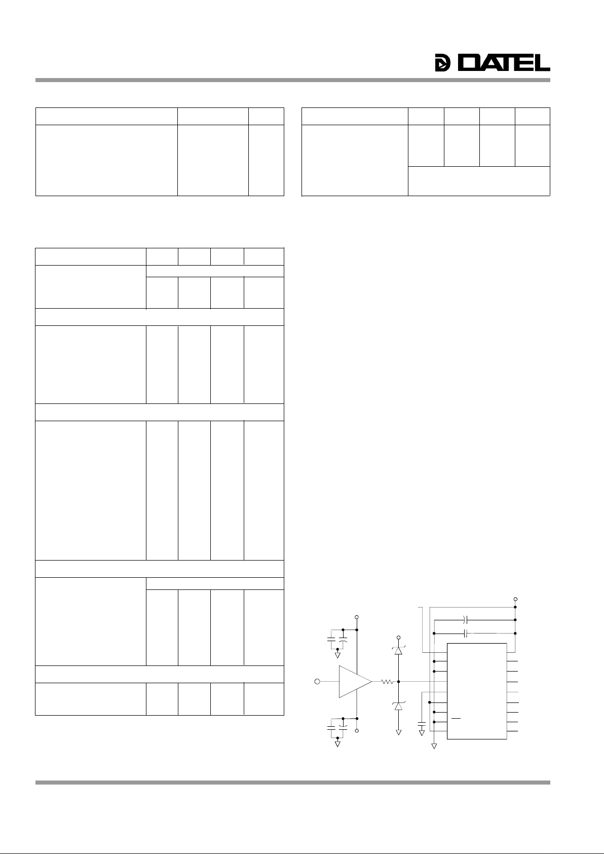
1. Input Buffer Amplifier – Since the ADC-207 has a switched
capacitor type input, the input impedance of the 207 is
dependent on the clock frequency. At relatively slow
conversion rates, a general purpose type input buffer can be
used; at high conversion rates DATEL recommends either
the HA-5033 or Elantec 2003. See Figure 2 for typical
connections.
2. Reference Ladder – Adjusting the voltage at +REFERENCE
adjusts the gain of the ADC-207. Adjusting the voltage at –
REFERENCE adjusts the offset or zero of the ADC-207.
The midpoint pin is usually bypassed to ground through a
0.1µF capacitor, although it can be tied to a precision
voltage halfway between +REFERENCE and
–REFERENCE. This would improve integral linearity
beyond 7 bits.
3. Clock Pulse Width – To improve performance at Nyquist
bandwidths, the clock duty cycle can be adjusted so that the
low portion of the clock pulse is 12ns wide. The smaller
aperture allows the ADC-207 to closely resemble an ideal
sampler. See Figure 4.
4. At sampling rates less than 100kHz, there may be some
degradation in offset and differential nonlinearity.
Performance may be improved by increasing the clock duty
cycle (decreasing the time spent in the sample mode).
CAUTION
Since the ADC-207 is a CMOS device, normal precautions
against static electricity should be taken. Use ground straps,
grounded mats, etc. The Absolute Maximum Ratings of the
device MUST NOT BE EXCEEDED as irrevocable damage to
the ADC-207 will occur.
ABSOLUTE MAXIMUM RATINGS
PARAMETERS LIMITS UNITS
Power Supply Voltage (+V
DD
) –0.5 to +7 Volts
Digital Inputs –0.5 to +5.5 Volts
Analog Input –0.5 to (+V
DD
+0.5) Volts
Reference Inputs –0.5 to +V
DD
Volts
Digital Outputs –0.5 to +5.5 Volts
(short circuit protected to ground)
Lead Temperature (10 sec. max.) +300 °C
Figure 2. Typical Connections for Using the ADC-207
FUNCTIONAL SPECIFICATIONS
(Typical at +5V power, +25°C, 20MHz clock, +REFERENCE = +5V,
–REFERENCE = ground, unless noted)
ANALOG INPUT MIN. TYP. MAX. UNITS
Input Type Single-ended, non-isolated
Input Range (dc-20MHz) 0 — +5 Volts
Input Impedance — 1000 — Ohms
Input Capacitance
(Full Range) — 10 — pF
DIGITAL INPUTS
Logic Levels
Logic "1" +3.2 — — Volts
Logic "0" — — +0.8 Volts
Logic Loading "1" — ±1 ±5 microamps
Logic Loading "0" — ±1 ±5 microamps
Sample Pulse Width
(During Sampling Portion of Clock) 12 — — ns
Reference Ladder Resistance 225 330 — Ohms
PERFORMANCE
Conversion Rate
➀ 20 25 — MHz
Harmonic Distortion ➁
(8MHz 2nd Order Harmonic) — –40 — dB
Differential Gain ➂ — 3 — %
Differential Phase ➂ — 1.5 — degrees
Aperture Delay — 8 — ns
Aperture Jitter — 50 — ps
No Missing Codes
LC/MC grade 0 — +70 °C
LM/MM grade –55 — +125 °C
Integral Linearity ➃ — ±0.8 ±1 LSB
Over Temperature Range — ±1 — LSB
Differential Nonlinearity — ±0.3 ±0.5 LSB
Over Temperature Range — ±0.4 ±0.6 LSB
Power Supply Rejection — ±0.02 —
%FSR/%Vs
DIGITAL OUTPUTS
Data Coding Straight binary
Data Output Resolution 7 — — Bits
Logic Levels
Logic "1" +2.4 +4.5 — Volts
Logic "0" (at 1.6mA) — — +0.4 Volts
Logic Loading "1" –4 — — mA
Logic Loading "0" +4 — — mA
Output Data Valid Delay
(From Rising Edge) — 15 17 ns
POWER REQUIREMENTS
Power Supply Range (+V
DD
) +3.0 +5.0 +5.5 Volts
Power Supply Current — +50 +70 mA
Power Dissipation — 250 385 mW
Footnotes:
➀ At full power input and chip selects enabled.
➁ At 4MHz input and 20MHz clock.
➂ For 10-step, 40 IRE NTSC ramp test.
➃ Adjustable using reference ladder midpoint tap. See ADC-207 Operation.
(MSB)
0.1µF
0.1µF
4.7µF
0.01µF
+5V
+15
+
+
–15
47µF
11
12
10
5
HA-5033
10
Ω
+5V
20MHz
CLOCK
(LSB)B7
B6
B5
B4
B3
B2
B1
OF
OF
B1
B2
B3
B4
B5
B6
B7
+V
DD
CS2
CS1
+REFERENCE
MID
V
IN
–REFERENCE
DIGITAL GND
ANALOG GND
CLOCK
181
2
3
4
5
6
7
8
9
0.1µF
+
47µF
17
16
15
14
13
12
11
10
2
Page 3

ADC-207
® ®
OUTPUT CODING
(+REFERENCE = +5.12V, –REFERENCE = ground, MIDPOINT = no connection)
NOTE: The reference should be held to ±0.1% accuracy or
better. Do not use the +5V power supply as a
reference input without precision regulation and high
frequency decoupling.
Values shown here are for a +5.12V reference. Scale other
references proportionally. Calibration equipment should test for
code changes at the midpoints between these center values
shown in Table 1. For example, at the half-scale major carry,
set the input to 2.54V and adjust the reference until the code
flickers equally between 63 and 64. Note also that the
weighting for the comparator resistor network leaves the first
and last thresholds within 1/2LSB of the end points to adjust
the code transition to the proper midpoint values.
Continuous conversion requires one cycle/sample (one positive
pulse and one negative pulse). The 3-state buffer has two
enable lines, CS1 and CS2. Table 2 shows the truth table for
chip select signals. CS1 has the function of enabling/disabling
bits 1 through 7. CS2 has the function of enabling/disabling
bits 1 through 7 and the overflow bit. Also, a full-scale input
produces all ones, including the overflow bit at the output. The
ADC-207 has an adjustable resistor ladder string. The top end,
idle point, and bottom end are brought out for use with
applications circuits.
These pins are called +REFERENCE, MIDPOINT and
–REFERENCE, respectively. In typical operation
+REFERENCE is tied to +5V, –REFERENCE is tied to ground,
and MIDPOINT is bypassed to ground. Such a configuration
results in a 0 to +5V input voltage range. The MIDPOINT pin
can also be tied to a +2.5V source to further improve integral
linearity. This is usually not necessary unless better than 7-bit
linearity is needed.
Table 2. Chip Select Truth Table
CS1 CS2 Bits 1-7 Overflow Bit
0 0 3-State Mode 3-State Mode
1 0 3-State Mode 3-State Mode
0 1 Data Outputed Data Outputed
1 1 3-State Mode Data Outputed
NOTE: Reduce the sample time (sample pulse)
ADC-207 OPERATION
The ADC-207 uses a switched capacitor scheme in which
there is an auto-zero phase and a sampling phase. See
Figure 1 and Timing Diagram. The ADC-207 uses a single
clock input. When the clock is at a high state (logic 1), the
ADC-207 is in the auto-zero phase (Ø1). When the clock is at
a low state (logic 0), the ADC-207 is in the sampling phase
(Ø2). During phase 1, the 128 comparator outputs are shorted
to their inputs through CMOS switches. This serves the
purpose of bringing the inputs and outputs to the transition
levels of the respective comparators. The inputs to the
comparators are also connected to 128 sampling capacitors.
The other end of the 128 capacitors are also shorted to 128
taps of a resistor ladder, via CMOS switches. Therefore, during
phase 1 the sampling capacitors are charged to the differential
voltage between a resistor tap and its respective comparator
transition voltage.
This eliminates offset differences between comparators and
yields better temperature performance. During phase 2 (Ø2) the
input voltage is applied to the 128 capacitors, via CMOS
switches. This forces the comparators to trip either high or low.
Since the comparators during phase 1 were sitting at their
transition point, they can trip very quickly to the correct state.
Also during phase 2, the outputs of the comparators are loaded
into internal latches which in turn feed a128-to-7 encoder. When
going back into phase 1, the output of the encoder is loaded into
an output latch. This latch then feeds the 3-state output buffer.
This means that the ADC-207 is of pipeline design. To do a
single conversion, the ADC-207 requires a positive pulse
followed by a negative pulse followed by a positive pulse.
Table 1. ADC-207 Output Coding
Analog Input 1 2 3 4 5 6 7 Hexadecimal
(Center Value) Code Overflow MSB LSB Decimal (Incl. 0V)
0.00V Zero 0 0 0 0 0 0 0 0 0 00
+0.04V +1LSB 0 0 0 0 0 0 0 1 1 01
+1.28V +1/4FS 0 0 1 0 0 0 0 0 32 20
+2.52V +1/2FS – 1LSB 0 0 1 1 1 1 1 1 63 3F
+2.56V +1/2FS 0 1 0 0 0 0 0 0 64 40
+2.60V +1/2FS + 1LSB 0 1 0 0 0 0 0 1 65 41
+3.84V +3/4FS 0 1 1 0 0 0 0 0 96 60
+5.08V +FS 0 1 1 1 1 1 1 1 127 7F
+5.12V Overflow 1 1 1 1 1 1 1 1 255* FF
*Note that the overflow code does not clear the data bits.
CLOCK
OUTPUT
DATA
AUTO
ZERO
N DATA
N+1 DATA
SAMPLE
N
SAMPLE
N + 1
SAMPLE
N + 2
AUTO
ZERO
AUTO
ZERO
17ns max.17ns max.
∅1
∅2 ∅1 ∅1∅2 ∅2
TIMING DIAGRAM
3
Page 4

ADC-207
® ®
USING TWO ADC-207’S FOR 8-BIT RESOLUTION
Two ADC-207’s (A and B) are cascadable for applications
requiring 8-bit resolution. The device A provides a typical 7-bit
output. The OVERFLOW signal of device A turns off device A
and turns on the device B. The OVERFLOW signal of device A
is also used as MSB for 8-bit operation. The device B provides
the other seven bits from the input signal. Figure 4 shows the
circuit connections for the application.
BEAT FREQUENCY AND ENVELOPE TESTS
Figure 5 shows an actual ADC-207 plot of the Beat Frequency
Test. This test uses a 20MHz clock input to the ADC-207 with
a 20.002MHz full-scale sine wave input. Although the
converter would not normally be used in this mode because
the input frequency violates Nyquist criteria for full recovery of
signal information, the test is an excellent demonstration of the
ADC-207’s high-frequency performance.
The effect of the 2kHz frequency difference between the input
and the clock is that the output will be a 2kHz sinusoidal digital
data array which "walks" along the actual input at the 2kHz
beat note frequency. Any inability to follow the 20.002MHz
input will be immediately obvious by plotting the digital data
array. Further arithmetic analysis may be done on the data
array to determine spectral purity, harmonic distortion, etc.
This test is an excellent indication of:
1. Full power input bandwidth of all 128 comparators.
(Any gain loss would show as signal distortion.)
2. Phase response linearity vs. instantaneous signal
magnitude. (Phase problems would show as
improper codes.)
3. Comparator slew rate limiting.
Figure 6 shows an actual ADC-207 plot of the Envelope Test.
This test is a variation of the previous test but uses a
10.002MHz sinewave input to give two overlapping cycles
when the data is reconstructed by a D/A converter output to an
oscilloscope. The scope is triggered by the 20MHz clock used
by the A/D. Any asymmetry between positive and negative
portions of the signal will be very obvious. This test is an
excellent indication of slew rate capability. At the peaks of the
envelope, consecutive samples swing completely through the
input voltage range.
to 12ns to improve performance above
20MHz. Such a configuration will closely
resemble an ideal sampler.
Figure 3. Optional Pulse Shaping Circuit
Figure 4. Using Two ADC-207’s for 8-Bit Operation
NOTE: The output data bit numbering is offset
by a bit to the device B’s output.
9
CLOCK IN
GROUND
+5 VOLTS
8
1
2
3
13
12
11
CLOCK OUT
20k
6
4
5
0.01µF
10pF
18
6
10
TURN
+5V
8
4
1
9
3
6
8
1
4
+5V
REFERENCE
GROUND
9
18
3
7
7
10
OVERFLOW
ANALOG IN
CLOCK IN
OPTIONAL
MIDSCALE
ADJUST
+5.12
REFERENCE
IN
BIT 1 (MSB)
BIT2
BIT3
BIT4
BIT5
BIT6
BIT7
BIT8 (LSB)
11
12
13
14
15
16
17
+REFERENCE
+V
DD
OF
B1
B2
B3
B4
B5
B6
B7
DIG GND
CS1
ANALOG INPUT
CLOCK
CS2
–REFERENCE
ANALOG GROUND
+REFERENCE
OF
B1
B2
B3
B4
B5
B6
B7
CS1
CLOCK
ANALOG INPUT
+V
DD
CS2
–REFERENCE
2
10
11
12
13
14
15
16
17
2
ANALOG GROUND
DIG GND
Page 5

ADC-207
® ®
0 1 2 3 4 5 6 7 8 9 10
FREQUENCY (MHz)
70
65
60
55
50
45
40
35
30
25
20
15
10
5
0
–5
–10
AMPLITUDE (dB)
69.2
27.3
SAMPLE PULSE WIDTH = 25ns
4MHz FUNDAMENTAL
Figure 5. Beat Frequency Test at 20MHz
Figure 6. 10MHz Envelope Test
FFT TEST
This test actually produces an amplitude versus frequency graph (Figure 7) which indicates harmonic distortion and signal-to-noise
ratio. The theoretical rms signal-to-noise ration for a 7-bit converter is +43.8dB.
Figure 7. FFT Test Using the ADC-207
0 1 2 3 4 5 6 7 8 9 10
70
65
60
55
50
45
40
35
30
25
20
15
10
0
–5
–10
SAMPLE PULSE = 25ns
69.2
27.3
4MHz FUNDAMENTAL
0 0.2 0.4 0.6 0.8 1 1.2 1.4 1.6 1.8 2
NUMBER OF SAMPLES(X10 )
3
OUTPUT
CODES
120
110
100
90
80
70
60
50
40
30
20
10
0
OUTPUT
CODES
120
110
100
90
80
70
60
50
40
30
20
10
0
0 0.1 0.2 0.3 0.4 0.5 0.6 0.7 0.8 0.9 1 1.1 1.2 1.3 1.4 1.5
NUMBER OF SAMPLES(X10 )
3
Page 6

MECHANICAL DIMENSIONS INCHES (MM)
ORDERING INFORMATION
MODEL TEMP. RANGE PACKAGE
ADC-207MC 0 to +70°C 18-pin DIP
ADC-207MM –55 to +125°C 18-pin DIP
ADC-207MM-QL –55 to +125°C 18-pin DIP
ADC-207LC 0 to +70°C 24-pin CLCC
ADC-207LM –55 to +125°C 24-pin CLCC
ADC-207LM-QL –55 to +125°C 24-pin CLCC
ACCESSORIES
ADC-B207/208 Evaluation Board for DIP Version
(without ADC-207)
0.400
(10.16 )
0.250 ±0.005
(6.35 ±0.13)
0.050
(1.270)
TYP.
0.020 ±0.005
(0.51 ±0.13)
1
24
16
10
4
0.090 MAX.
(2.29 MAX.)
+0.010
–0.005
+0.25
–0.13
0.400
(10.16 )
+0.010
–0.005
+0.25
–0.13
0.250 ±0.005
(6.35 ±0.13)
PIN 1
INDEX
TOP VIEW
24-Pin Ceramic LCC
18-Pin Ceramic DIP
0.960 MAX.
(24.38 MAX.)
0.220 / 0.310
(5.59 / 7.87)
DATEL
ADC-207MC
PIN 1
IDENTIFIER
1
18
10
9
0.200 MAX.
(5.1 MAX.)
0.100 TYP.
(2.540)
0.014 / 0.023
(0.35 / 0.58)
0.015 / 0.060
(0.38 /1.52)
0.290 / 0.320
(7.36 / 8.13)
SEATING
PLANE
0.035
(0.889)
0.008 / 0.015
(0.20 / 0.38)
INNOVATION and EX C ELL E N C E
® ®
DATEL makes no representation that the use of its products in the circuits described herein, or the use of other technical information contained herein, will not infringe upon existing or future patent rights. The descriptions contained herein
do not imply the granting of licenses to make, use, or sell equipment constructed in accordance therewith. Specifications are subject to change without notice. The DATEL logo is a registered DATEL, Inc. trademark.
DS-0038B 10/96
ISO 9001
ISO 9001
REGISTERED
ADC-207
® ®
DATEL, Inc. 11 Cabot Boulevard, Mansfield, MA 02048-1151
Tel: (508) 339-3000 (800) 233-2765 Fax: (508) 339-6356
Internet: www.datel.com E-mail:sales@datel.com
Data Sheet Fax Back: (508) 261-2857
DATEL (UK) LTD. Tadley, England Tel: (01256)-880444
DATEL S.A.R.L. Montigny Le Bretonneux, France Tel: 1-34-60-01-01
DATEL GmbH München, Germany Tel: 89-544334-0
DATEL KK Tokyo, Japan Tel: 3-3779-1031, Osaka Tel: 6-354-2025
 Loading...