DATEL ADC-207MM-QL, ADC-207MM, ADC-207MC, ADC-207LM-QL, ADC-207LM Datasheet
...
INNOVATION and EX C ELL E N C E
® ®
INPUT/OUTPUT
CONNECTIONS
DIP LCC
PINS FUNCTION PINS
1 CLOCK INPUT 1
2 DIGITAL GROUND 4
3 –REFERENCE 5
4 ANALOG INPUT 6
5 MIDPOINT 7
6 +REFERENCE 8
7 ANALOG GROUND 9
8 CS1 11
9 CS2 12
10 OVERFLOW 13
11 BIT 1 (MSB) 14
12 BIT 2 16
13 BIT 3 17
14 BIT 4 19
15 BIT 5 20
16 BIT 6 21
17 BIT 7 (LSB) 23
18 +5V
SUPPLY 24
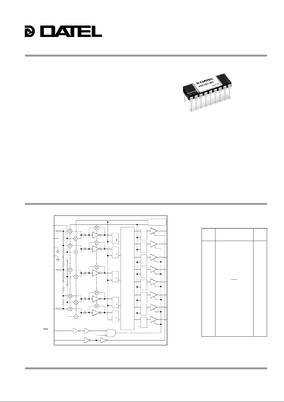
Figure 1. ADC-207 Functional Block Diagram (DIP Pinout)
FEATURES
• 7-bit flash A/D converter
• 20MHz sampling rate
• Low power (250mW)
• Single +5V supply
• 1.2 micron CMOS technology
• 7-bit latched 3-state output with overflow bit
• Surface-mount versions
• High-reliability version
• No missing codes
GENERAL DESCRIPTION
The ADC-207 is the industry’s first 7-bit flash converter using an
advanced high-speed VLSI 1.2 micron CMOS process. This
process offers some very distinctive advantages over other
processes, making the ADC-207 unique. The smaller
geometrics of the process achieve high speed, better linearity
and superior temperature performance.
Since the ADC-207 is a CMOS device, it also has very low
power consumption (250mW). The device draws power from
a single +5V supply and is conservatively rated for 20MHz
operation. The ADC-207 allows using sampling apertures as
small as 12ns, making it more closely approach an ideal
sampler. The small sampling apertures also let the device
operate at greater than 20MHz.
The ADC-207 has 128 comparators which are auto-balanced
on every conversion to cancel out any offsets due to
temperature and/or dynamic effects. The resistor ladder has a
midpoint tap for use with an external voltage source to improve
integral linearity beyond 7 bits. The ADC-207 also provides the
user with 3-state outputs for easy interfacing to other
components.
There are six models of the ADC-207 covering two operating
temperature ranges, 0 to +70°C and –55 to +125°C. Two highreliability "QL" models are also available.
D
G Q
D
G Q
D
G QDG Q
D
G QDG Q
D
G
Q
D
G
Q
DGQ
DGQ
D
G
Q
D
G
Q
D
G
Q
DGQ
ANALOG INPUT 4
+REFERENCE 6
DIGITAL GROUND 2
ANALOG GROUND 7
RANGE MIDPOINT 5
R/2
R
R
R
R
R/2
R/2
–REFERENCE 3
CS1
8
9
+5V SUPPLY 18
+VDD
1 CLOCK INPUT
CLOCK
GENERATOR
10 OVERFLOW
11 BIT 1 (MSB)
12 BIT 2
13 BIT 3
14 BIT 4
15 BIT 5
16 BIT 6
17 BIT 7 (LSB)
128-TO-7
ENCODER
CS2
D
G QDG Q
D
G QDG Q
∅1
∅2 ∅2
∅1
ADC-207
7-Bit, 20MHz, CMOS
Flash A/D Converters
DATEL, Inc., 11 Cabot Boulevard, Mansfield, MA 02048-1151 (U.S.A.) • Tel: (508) 339-3000 Fax: (508) 339-6356 • For immediate assistance (800) 233-2765

ADC-207
® ®
PHYSICAL/ENVIRONMENTAL
PARAMETERS MIN. TYP. MAX. UNITS
Operating Temp. Range, Case:
LC/MC Versions 0 — +70 °C
MM/LM/QL Versions –55 — +125 °C
Storage Temp. Range –65 — +150 °C
Package Type
DIP 18-pin ceramic DIP
LCC 24-pin ceramic LCC
TECHNICAL NOTES
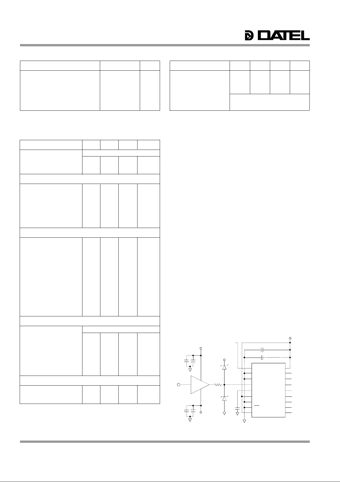
1. Input Buffer Amplifier – Since the ADC-207 has a switched
capacitor type input, the input impedance of the 207 is
dependent on the clock frequency. At relatively slow
conversion rates, a general purpose type input buffer can be
used; at high conversion rates DATEL recommends either
the HA-5033 or Elantec 2003. See Figure 2 for typical
connections.
2. Reference Ladder – Adjusting the voltage at +REFERENCE
adjusts the gain of the ADC-207. Adjusting the voltage at –
REFERENCE adjusts the offset or zero of the ADC-207.
The midpoint pin is usually bypassed to ground through a
0.1µF capacitor, although it can be tied to a precision
voltage halfway between +REFERENCE and
–REFERENCE. This would improve integral linearity
beyond 7 bits.
3. Clock Pulse Width – To improve performance at Nyquist
bandwidths, the clock duty cycle can be adjusted so that the
low portion of the clock pulse is 12ns wide. The smaller
aperture allows the ADC-207 to closely resemble an ideal
sampler. See Figure 4.
4. At sampling rates less than 100kHz, there may be some
degradation in offset and differential nonlinearity.
Performance may be improved by increasing the clock duty
cycle (decreasing the time spent in the sample mode).
CAUTION
Since the ADC-207 is a CMOS device, normal precautions
against static electricity should be taken. Use ground straps,
grounded mats, etc. The Absolute Maximum Ratings of the
device MUST NOT BE EXCEEDED as irrevocable damage to
the ADC-207 will occur.
ABSOLUTE MAXIMUM RATINGS
PARAMETERS LIMITS UNITS
Power Supply Voltage (+V
DD
) –0.5 to +7 Volts
Digital Inputs –0.5 to +5.5 Volts
Analog Input –0.5 to (+V
DD
+0.5) Volts
Reference Inputs –0.5 to +V
DD
Volts
Digital Outputs –0.5 to +5.5 Volts
(short circuit protected to ground)
Lead Temperature (10 sec. max.) +300 °C
Figure 2. Typical Connections for Using the ADC-207
FUNCTIONAL SPECIFICATIONS
(Typical at +5V power, +25°C, 20MHz clock, +REFERENCE = +5V,
–REFERENCE = ground, unless noted)
ANALOG INPUT MIN. TYP. MAX. UNITS
Input Type Single-ended, non-isolated
Input Range (dc-20MHz) 0 — +5 Volts
Input Impedance — 1000 — Ohms
Input Capacitance
(Full Range) — 10 — pF
DIGITAL INPUTS
Logic Levels
Logic "1" +3.2 — — Volts
Logic "0" — — +0.8 Volts
Logic Loading "1" — ±1 ±5 microamps
Logic Loading "0" — ±1 ±5 microamps
Sample Pulse Width
(During Sampling Portion of Clock) 12 — — ns
Reference Ladder Resistance 225 330 — Ohms
PERFORMANCE
Conversion Rate
➀ 20 25 — MHz
Harmonic Distortion ➁
(8MHz 2nd Order Harmonic) — –40 — dB
Differential Gain ➂ — 3 — %
Differential Phase ➂ — 1.5 — degrees
Aperture Delay — 8 — ns
Aperture Jitter — 50 — ps
No Missing Codes
LC/MC grade 0 — +70 °C
LM/MM grade –55 — +125 °C
Integral Linearity ➃ — ±0.8 ±1 LSB
Over Temperature Range — ±1 — LSB
Differential Nonlinearity — ±0.3 ±0.5 LSB
Over Temperature Range — ±0.4 ±0.6 LSB
Power Supply Rejection — ±0.02 —
%FSR/%Vs
DIGITAL OUTPUTS
Data Coding Straight binary
Data Output Resolution 7 — — Bits
Logic Levels
Logic "1" +2.4 +4.5 — Volts
Logic "0" (at 1.6mA) — — +0.4 Volts
Logic Loading "1" –4 — — mA
Logic Loading "0" +4 — — mA
Output Data Valid Delay
(From Rising Edge) — 15 17 ns
POWER REQUIREMENTS
Power Supply Range (+V
DD
) +3.0 +5.0 +5.5 Volts
Power Supply Current — +50 +70 mA
Power Dissipation — 250 385 mW
Footnotes:
➀ At full power input and chip selects enabled.
➁ At 4MHz input and 20MHz clock.
➂ For 10-step, 40 IRE NTSC ramp test.
➃ Adjustable using reference ladder midpoint tap. See ADC-207 Operation.
(MSB)
0.1µF
0.1µF
4.7µF
0.01µF
+5V
+15
+
+
–15
47µF
11
12
10
5
HA-5033
10
Ω
+5V
20MHz
CLOCK
(LSB)B7
B6
B5
B4
B3
B2
B1
OF
OF
B1
B2
B3
B4
B5
B6
B7
+V
DD
CS2
CS1
+REFERENCE
MID
V
IN
–REFERENCE
DIGITAL GND
ANALOG GND
CLOCK
181
2
3
4
5
6
7
8
9
0.1µF
+
47µF
17
16
15
14
13
12
11
10
2
 Loading...