

Page 1
FIXED 2.5 AND 5 VOLT
3-TERMINAL VOLTAGE REFERENCES
ISSUE 4 - MARCH 1998
ZTR250
ZTR500
DEVICE DESCRIPTION
The ZTR250 and ZTR500 are precision three
terminal references. These devices are ideal
for battery powered applications where
power saving is important. They offer low
power alternatives to other two terminal
shunt references.
The ZTR devices do not require an external
resistor and, in contrast to two terminal
references, waste none of the battery power
as load current varies. The ZTR only
consumes 30µA supply current.
The two devices require as low as 1.4 volts
between input and output for regulation.
Output voltage tolerance is ± 2.5%, with a
voltage variation of 0.275mV/°C over the
-55°C to 125°C operating range.
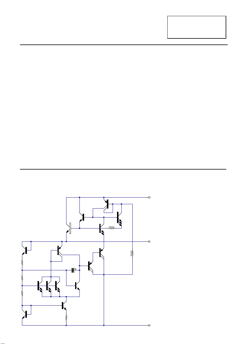
SCHEMATIC DIAGRAM
FEATURES
Small outline SOT23 and SOT89
•
packages
TO92 package
•
2.5V and 5V output
•
2.5% tolerance
•
Supply current independent of input
•
voltage over temperature
Output current up to 50mA
•
Very low supply current (30µA)
•
Unconditionally stable
•
Internal short circuit current limit
•
APPLICATIONS
Battery Powered Systems
•
Portable and Hand Held Equipment
•
Instrumentation
•
Metering
•
Vin
Vout
Gnd
4-388
Page 2

ZTR250
ZTR500
ABSOLUTE MAXIMUM RATINGS
Input Voltage 20V
Output current (I
) 200mA
O
Operating temperature -55 to 125°C
Storage temperature -65 to 150°C
Power Dissipation (T
SOT23 500mW
TO92 600mW
SOT89 1.5W
Note:
1. The maximum operating input voltage and output current of the device will be governed by the maximum
power dissipation of the selected package. Maximum package power dissipation is specified at 25 °C and
must be linearly derated to zero at T
2. The following data represents pulse test conditions with junction temperatures as indicated at the initiation
of the test. Continuous o peration of the devices with the stated conditions might exceed the po wer dissipation
limits of the chosen package.
3. This device does not contain a thermal shutdown circuit so care should be taken not to exceed the stated
maximum power dissipation rating.Maximum power dissipation, for the SOT23 and SOT89 packages, is
calculated assuming that the device is mounted on a ceramic substrate measuring 15 x 15 x 0.6mm.
amb
=125°C.
ZTR250
ELECTRICAL CHARACTERISTICS
TEST CONDITIONS (Unless otherwise stated):T
SYMBOL PARAMETER CONDITIONS MIN. TYP. MAX. UNITS
V
Output Voltage 2.438 2.5 2.563 V
O
I
=0 to 50mA
O
T
=-55 to 125°C
j
V
=4.5 to 20V
in
I
=0 to 50mA
O
T
=-55 to 125°C
j
∆V
Line Regulation Vin=4.5 to 20V 5 15 mV
O
∆V
Load Regulation IO=0 to 50mA
O
l
s
∆l
s
V
n
∆Vin/∆V
V
in
∆VO/∆T
Supply Current Tj=-55 to 125°C 30 40
Supply Current Change IO=0 to 50mA
Output Noise Voltage f=10Hz to 10kHz 65
Ripple Rejection Vin=6.3 to 18V
O
Input Voltage Required
To Maintain Regulation 4.2 3.9 V
Average Temperature
Coefficient of V
O
I
=0 to 10mA
O
V
=4.5 to 20V
in
f=120Hz 55 75 dB
IO=5.0mA
T
=-55 to 125°C 0.275 0.700 mV/°C
j
=25°C, IO=10mA, Vin=6.5V
j
2.360 2.640 V
2.360 2.640 V
20
12
1
2
amb
= 25°C, T
=150 °C)
jmax
30 mV
mV
µA
±10
10
µA
µA
µV
(rms)
4-389
Page 3

ZTR250
ZTR500
ZTR500
ELECTRICAL CHARACTERISTICS
TEST CONDITIONS (Unless otherwise stated):T
SYMBOL PARAMETER CONDITIONS MIN. TYP. MAX. UNITS
V
Output Voltage 4.875 5 5.125 V
O
I
=0 to 50mA
O
T
=-55 to 125°C
j
V
=7 to 20V
in
I
=0 to 50mA
O
T
=-55 to 125°C
j
∆V
Line Regulation Vin=7 to 20V 5 15 mV
O
∆V
Load Regulation IO=0 to 50mA
O
l
s
∆l
s
V
n
∆Vin/∆V
V
in
∆VO/∆T
Supply Current Tj=-55 to 125°C 50 70
Supply Current Change IO=0 to 50mA
Output Noise Voltage f=10Hz to 10kHz 90
Ripple Rejection Vin=8 to 18V
O
Input Voltage Required
To Maintain Regulation 7 6.7 V
Average Temperature
Coefficient of V
O
I
=0 to 10mA
O
V
=7 to 20V
in
f=120Hz
IO=5.0mA
=-55 to 125°C 0.275 0.700 mV/°C
T
j
=25°C, IO=10mA, Vin=10V
j
4.780 5.160 V
4.780 5.175 V
25
40 mV
15
1
2
±10
10
55 72
mV
µA
µA
µA
µV
(rms)
dB
4-390
Page 4

ZTR250
ZTR500
TYPICAL CHARACTERISTICS
Output Voltage
Supply Current (µA)
5.02
5.00
4.98
4.96
2.52
2.50
2.48
2.46
34
32
30
28
26
b
a
-25025 50
-50
Temperature (°C)
Output Voltage Temperature
a
-50 -25
02550
Temperature (°C)
Supply Current v Temperature
Io=5mA
V
Io=5mA
V
75 100
Io=0
V
in=Vo+4
75
in=Vo+4
in=Vo+4
125
125100
a=ZTR250: b=ZTR500
60
50
40
10
a
12 14 16
Supply Current (µA)
30
20
10
0
468
2
Input Voltage (V)
Supply Current v Voltage
60
56
52
Supply Current (µA)
48
44
40
-50
-25025 50
b
Temperature (°C)
Supply Current v Temperature
b
75 100
Io=10mA
Io=0
in=Vo+4
V
125
20
18
50
b
Supply Current (µA)
49
48
47
30
a
29
28
27
0.1
1
Output Current
10
Io=0
V
in=Vo
Io=0
in=Vo+4
V
Supply Current v Output Current
2.5
+4
100
2.0
1.5
1.0
Drop-Out Voltage (V)
0.5
0
-50 -25025 50
b
a
75 100
Io=10mA
125
Temperature (°C)
Drop-Out Voltage v Temperature
4-391
Page 5

ZTR250
ZTR500
TYPICAL CHARACTERISTICS
10
1.0
0.1
Output Impedance (Ohms)
0.01
100
1K 10K
Frequency (Hz)
Output Impedance v Frequency
Load Current
a
0.4
0
Output Voltage Deviation (V)
-0.4
0
b
20
Load Transient Response
40
Time (µs)
I = 10mA
O
I = 2mA
o
V = V + 4V
IN
C
OUT
V
IN=Vo
dI
/dt=1A/µs
o
60
OUT
=0
a=ZTR250: b=ZTR500
90
80
70
60
50
a
b
100K
40
30
20
Ripple Rejection (dB)
10
0
10 100
a
b
Io = 10mA
1K 10K 100K
Ripple Frequency (Hz)
Ripple Rejection v Ripple Frequency
5mA
0mA
0.4
0
-0.4
+4
100
80
0.4
0
Output Voltage Deviation (V)
-0.4
01020
Vin
a
b
30
Time (µs)
C
V
dV
OUT
IN=Vo
IN
=0
+4
/dt=5V/µs
40 50
5V
0V
0.4
0
-0.4
Line Transient Response
(mW)
Power Dissipation
2
Surface Mount Devices
SOT89
1
SOT23
0
-25025 50
-50
Power Derating
Temperature (°C)
75 100
125
4-392
(mW)
Power Dissipation
600
400
200
800
0
-50
TO92
Through Hole Device
-25025 50
Temperature (°C)
Power Derating
75 100
125
Page 6

CONNECTION DIAGRAMS
ZTR250
ZTR500
SOT23 Package Suffix – F
Top View
SOT89
Package Suffix – Z
Top View
ORDERING INFORMATION
Part
Number
ZTR250C02 2.5 TO92 ZTR25002
ZTR250F02 2.5 SOT23 25U
ZTR250Z02 2.5 SOT89 25U
ZTR500C02 2.5 TO92 ZTR50002
ZTR500F02 2.5 SOT23 50N
ZTR500Z02 2.5 SOT89 50N
Tol %Package Part Mark
TO92 Package Suffix – C
Bottom View
4-393
Page 7

 Loading...