

Page 1

Zilog
PRELIMINARY
FEATURES
■ Z8S180 MPU
- Code Compatible with Zilog Z80®/Z180™ CPU
- Extended Instructions
- Operating Frequency: 33 MHz/5V or 20 MHz/3.3V
- Two DMA Channels
- On-Chip Wait State Generators
- Two UART Channels
- Two 16-Bit Timer Counters
- On-Chip Interrupt Controller
- On-Chip Clock Oscillator/Generator
- Clocked Serial I/O Port
- Fully Static
- Low EMI Option
ZILOG INTELLIGENT PERIPHERAL
P
RELIMINARY PRODUCT SPECIFICATION
Z80182/Z8L182
ZILOG INTELLIGENT PERIPHERAL
CONTROLLER (ZIP™)
■ Two ESCC
■ Three 8-Bit Parallel I/O Ports
■ 16550 Compatible MIMIC Interface for
Direct Connection to PC, XT, AT Bus
■ 100-Pin Package Styles (QFP, VQFP)
(0.8 Micron CMOS 5120 Technology)
■ Individual WSG for RAMCS and ROMCS
™
Channels with 32-Bit CRC
Z80182/Z8L182
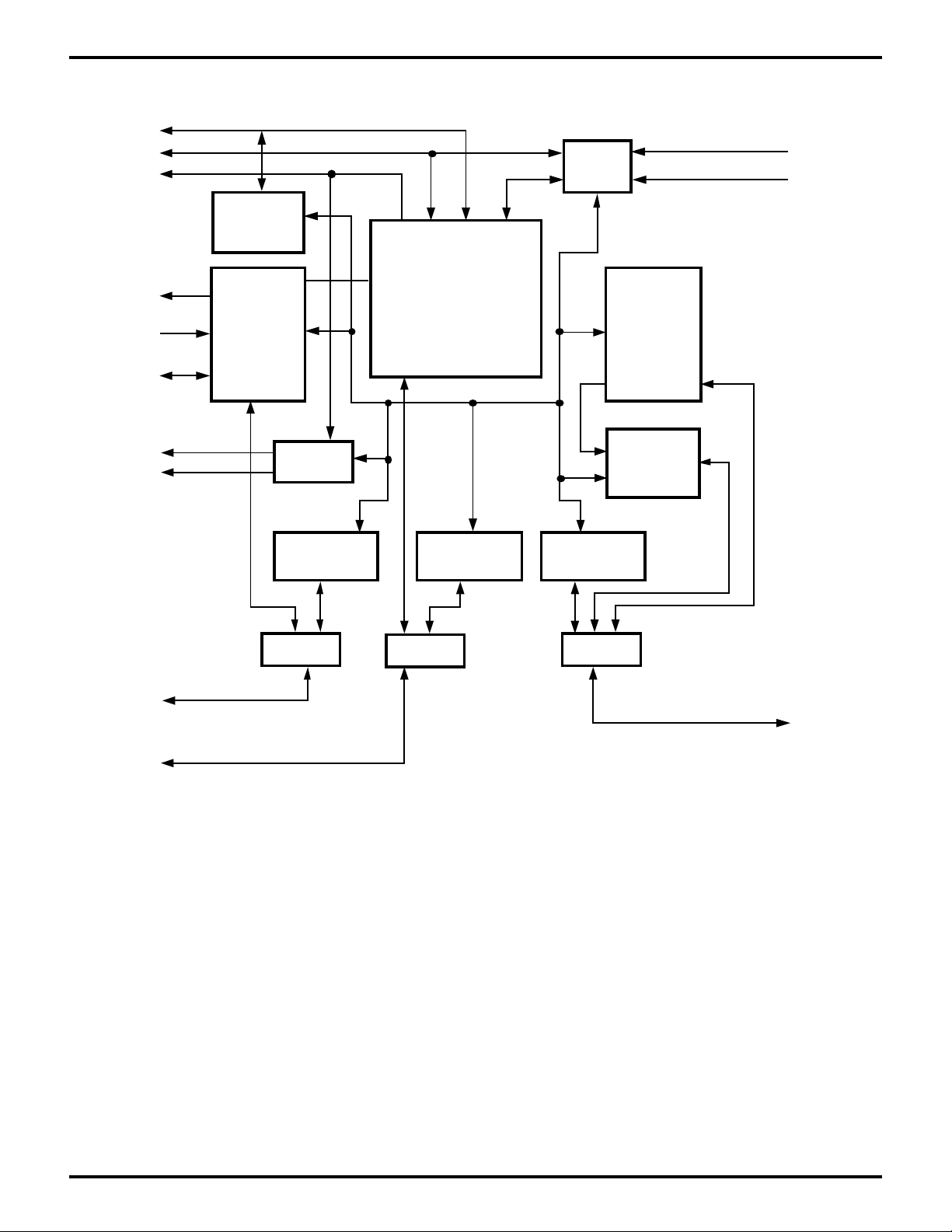
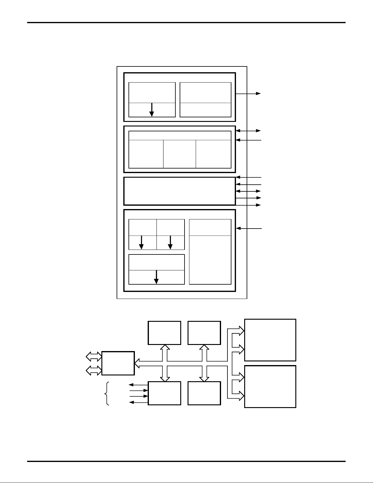
GENERAL DESCRIPTION
The Z80182/Z8L182 is a smart peripheral controller IC for
modem (in particular V. Fast applications), fax, voice
messaging and other communications applications. It
uses the Z80180 microprocessor (Z8S180 MPU core)
linked with two channels of the industry standard Z85230
ESCC (Enhanced Serial Communications Controller), 24
bits of parallel I/O, and a 16550 MIMIC for direct connection
to the IBM PC, XT, AT bus.
The Z80182/Z8L182 allows complete flexibility for both
internal PC and external applications. Also current PC
modem software compatibility can be maintained with the
Z80182/Z8L182 ability to mimic the 16550 UART chip. The
Z80180 acts as an interface between the ESCC™ and
16550 MIMIC interface when used in internal applications,
and between the two ESCC channels in the external
applications. This interface allows data compression and
error correction on outgoing and incoming data. In external
applications, three 8-bit parallel ports are available for
driving LEDs or other devices. Figure 1 shows the Z80182/
Z8L182 block diagram, while the pin assignments for the
QFP and the VQFP packages are shown in Figures 2 and
3, respectively. All references in this document to the
Z80182, or Z182 refer to both the Z80182 and Z8L182.
Notes:
All Signals with a preceding front slash, "/", are active Low, e.g.,
B//W (WORD is active Low); /B/W (BYTE is active Low, only).
Power connections follow conventional descriptions below:
Connection Circuit Device
Power V
Ground GND V
CC
V
DD
SS
DS971820600
3-1
Page 2
PRELIMINARYZilog
GENERAL DESCRIPTION (Continued)
D7-D0
Control
A19-A0
Bus
Transceiver
Tx Data
85230
Rx Data
ESCC
Control
ESCC
Channel
A
Z8S180
(Static Z80180)
MPU Core
GLU
Logic
/TRxCB
ZILOG INTELLIGENT PERIPHERAL
Z80182/Z8L182
EV1
EV2
85230
ESCC
Channel
B
/ROMCS
/RAMCS
85230
ESCC Ch. A
or Port C
Z180 Signals
or Port B
Address
Decode
8-Bit Parallel
Port C
MUX
8-Bit Parallel
MUX
Port B
8-Bit Parallel
Port A
MUX
16550
MIMIC
Interface
Note: Conventional use of the term "MPU side" refers to all interface through the Z180 MPU
core and "PC side" refers to all interface through the16550 MIMIC interface.
Figure 1. Z80182/Z8L182 Functional Block Diagram
16550 MIMIC
or ESCC
85230 Ch. B
and Port A
3-2
DS971820600
Page 3
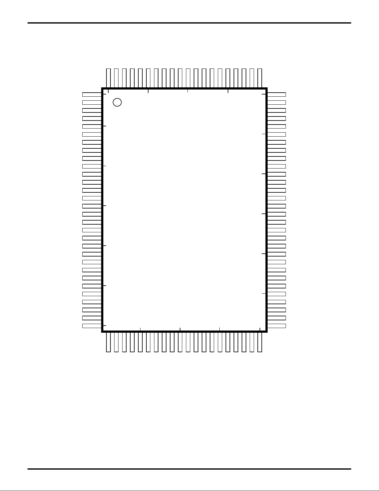
Zilog
/NMI
/RESET
/BUSREQ
PRELIMINARY
EXTAL
XTAL
VSS
PHI
/RD
/WR
/WAIT
/BUSACK
/IORQ
/M1E/MRD//MREQ
/RFSH
/HALT
/SYNCB//HCS
/RTXCB/HA2
RXDB/HA1
ZILOG INTELLIGENT PERIPHERAL
Z80182/Z8L182
/INT0
/INT1/PC6
/INT2/PC7
ST
A2
A3
A4
A5
A6
A9
A10
A11
A12
VSS
A13
A14
A15
A16
A17
A18/TOUT
VDD
A19
D0
D1
D2
D3
A0
A1
A7
A8
100
1
5
10
15
95
Z80182/Z8L182
90
85
100-Pin QFP
20
25
30
80
75
70
65
60
55
50454035
/TRXCB/HA0
TXDB//HDDIS
/CTSB//HWR
/DCDB//HRD
TXDA
/TRXCA
RXDA
VDD
IEI
/IOCS/IEO
VSS
/RTXCA
/SYNCA/PC4
/DCDA/PC0
/CTSA/PC1
/MWR/PC2//RTSA
/DTR//REQA/PC3
/W//REQA/PC5
PA7/HD7
PA6/HD6
PA5/HD5
PA4/HD4
PA3/HD3
PA2/HD2
PA1/HD1
PA0/HD0
EV2
EV1
/ROMCS
/RAMCS
DS971820600
D4D5D6
D7
/CTS0/PB1
/RTS0/PB0
TXA0/PB3
RXA0/PB4
/DCD0/PB2
RXA1/PB6
TXA1/PB5
RXS//CTS1/PB7
VSS
CKA1//TEND0
CKA0//DREQ0
VDD
/DREQ1
CKS//W//REQB//HTXRDY
TXS//DTR//REQB//HINTR
/TEND1//RTSB//HRXRDY
Figure 2. Z80182/Z8L182 100-Pin QFP Pin Configuration
3-3
Page 4
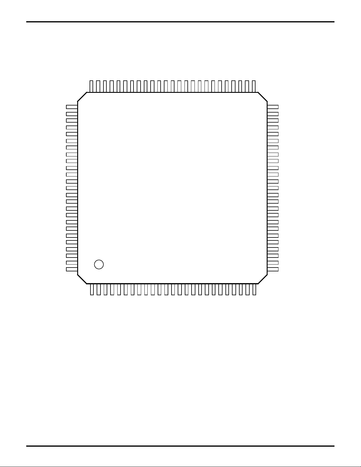
PRELIMINARYZilog
GENERAL DESCRIPTION (Continued)
ZILOG INTELLIGENT PERIPHERAL
Z80182/Z8L182
TXDB//HDDIS
/TRXCB/HA0
RXDB/HA1
/RTXCB/HA2
/SYNCB//HCS
/HALT
/RFSH
/IORQ
/MRD//MREQ
/M1
/WR
/RD
PHI
VSS
XTAL
EXTAL
/WAIT
/BUSACK
/BUSREQ
/RESET
/NMI
/INT0
/INT1/PC6
/INT2/PC7
TXDA
RXDA
/TRXCA
5
VDD
IEI
/IOCS/IEO
VSS
/RTXCA
Z80182/Z8L182
100-Pin VQFP
10 15 20
/SYNCA/PC4
/DCDA/PC0
/CTSA/PC1
/MWR/PC2//RTSA
/DTR//REQA/PC3
/W//REQA/PC5
PA7/HD7
6070 5565
PA6/HD6
PA5/HD5
PA4/HD4
PA3/HD3
PA2/HD2
PA1/HD1
EV2
PA0/HD0
50
45
40
35
30
26
EV1
/ROMCS
/RAMCS
/TEND1//RTSB//HRXRDY
VDD
/DREQ1
CKS//W//REQB//HTXRDY
TXS//DTR//REQB/HINTR
CKA1//TEND0
VSS
CKA0//DREQ0
RXS//CTS1/PB7
RXA1/PB6
TXA1/PB5
RXA0/PB4
TXA0/PB3
/DCD0/PB2
/CTS0/PB1
/RTS0/PB0
D7
D6
D5
D4
D3
D2
/DCDB//HRD
/CTSB//HWR
75 51
76
80
E
85
90
95
100
125
3-4
ST
A0A1A2
A3A4A5
A6A7A8
A9
A10
A11
A12
VSS
A13
A14
A15
A16
A17
A18/TOUT
VDD
A19
Figure 3. Z80182/Z8L182 100-Pin VQFP Pin Configuration
D0
D1
DS971820600
Page 5

Zilog
Z180 CPU SIGNALS
PRELIMINARY
ZILOG INTELLIGENT PERIPHERAL
Z80182/Z8L182
A19-A0.
A19-A0 form a 20-bit address bus. The Address Bus
provides the address for memory data bus exchanges up
to 1 Mbyte, and I/O data bus exchanges up to 64K. The
address bus enters a high impedance state during reset
and external bus acknowledge cycles, as well as during
SLEEP and HALT states. This bus is an input when the
external bus master is accessing the on-chip peripherals.
Address line A18 is multiplexed with the output of PRT
channel 1 (T
D7-D0.
D0 constitute an 8-bit bi-directional data bus, used for the
transfer of information to and from I/O and memory devices.
The data bus enters the high impedance state during reset
and external bus acknowledge cycles, as well as during
SLEEP and HALT states.
/RD.
that the CPU wants to read data from memory or an I/O
device. The addressed I/O or memory device should use
this signal to gate data onto the CPU data bus.
/WR.
that the CPU data bus holds valid data to be stored at the
addressed I/O or memory location.
Address Bus (input/output, active High, tri-state).
, selected as address output on reset).
OUT
Data Bus (bi-directional, active High, tri-state)
Read (input/output, active Low, tri-state).
Write (input/output, active Low, tri-state).
/RD indicates
/WR indicates
. D7-
/MRD.
/MRD is active when both the internal /MREQ and /RD are
active. /MRD is multiplexed with /MREQ on the /MRD
//MREQ pin. The /MRD//MREQ pin is an input during
adapter modes; is tri-state during bus acknowledge if
/MREQ function is selected; and is inactive High if /MRD
function is selected. The default function on power up is
/MRD and may be changed by programming bit 3 of the
Interrupt Edge/Pin MUX Register (xxDFH).
/MWR.
/MWR is active when both the internal /MREQ and /WR are
active. This /RTSA or PC2 combination is pin multiplexed
with /MWR on the /MWR/PC2//RTSA pin. The default function
of this pin on power up is /MWR, which may be changed by
programming bit 3 in the Interrupt Edge/Pin MUX Register
(xxDFH).
/WAIT.
MPU that the addressed memory or I/O devices are not
ready for a data transfer. This input is used to induce
additional clock cycles into the current machine cycle. The
/WAIT input is sampled on the falling edge of T2 (and
subsequent wait states). If the input is sampled Low, then
additional wait states are inserted until the /WAIT input is
sampled High, at which time execution will continue.
Memory Read (input/output, active Low, tri-state).
Memory Write (input/output, active Low, tri-state).
(input/output active Low).
/WAIT indicates to the
/IORQ.
/IORQ indicates that the address bus contains a valid I/O
address for an I/O read or I/O write operation. /IORQ is also
generated, along with /M1, during the acknowledgment of
the /INT0 input signal to indicate that an interrupt response
vector can be placed onto the data bus. This signal is
analogous to the IOE signal of the Z64180.
/M1.
with /MREQ, /M1 indicates that the current cycle is the
opcode fetch cycle of an instruction execution; unless
/M1E bit in the OMCR is cleared to 0. Together with /IORQ,
/M1 indicates that the current cycle is for an interrupt
acknowledge. It is also used with the /HALT and ST signals
to decode status of the CPU machine cycle. This signal is
analogous to the /LIR signal of the Z64180.
/MREQ.
state).
address for a memory read or memory write operation.
This signal is analogous to the /ME signal of the Z64180.
/MREQ is multiplexed with /MRD on the /MRD//MREQ pin.
The /MRD//MREQ pin is an input during adapter modes; is
tri-state during bus acknowledge if the /MREQ function is
selected; and is inactive High if /MRD function is selected.
I/O Request (input/output, active Low, tri-state).
Machine Cycle 1 (input/output, active Low).
Together
Memory Request (input/output, active Low, tri-
/MREQ indicates that the address bus holds a valid
/HALT.
output is asserted after the CPU has executed either the
HALT or SLEEP instruction, and is waiting for either nonmaskable or maskable interrupts before operation can
resume. It is also used with the /M1 and ST signals to
decode status of the CPU machine cycle. On exit of HALT/
SLEEP mode, the first instruction fetch can be delayed by
16 clock cycles after the /HALT pin goes High, if HALT 16
feature is selected.
/BUSACK.
/BUSACK indicates to the requesting device, the MPU
address and data bus, and some control signals, have
entered their high impedance state.
/BUSREQ.
used by external devices (such as DMA controllers) to
request access to the system bus. This request has a
higher priority than /NMI and is always recognized at the
end of the current machine cycle. This signal will stop the
CPU from executing further instructions and places the
address/data buses and other control signals, into the high
impedance state.
Halt/Sleep Status (input/output, active Low).
Bus Acknowledge (input/output, active Low).
Bus Request (input, active Low).
This input is
This
DS971820600
3-5
Page 6

Z180 CPU SIGNALS (Continued)
PRELIMINARYZilog
ZILOG INTELLIGENT PERIPHERAL
Z80182/Z8L182
/NMI.
triggered).
always recognized at the end of an instruction, regardless
of the state of the interrupt enable flip-flops. This signal
forces CPU execution to continue at location 0066H.
/INT0.
Low).
CPU will honor this request at the end of the current
instruction cycle as long as the /NMI and /BUSREQ signals
are inactive. The CPU acknowledges this interrupt request
with an interrupt acknowledge cycle. During this cycle,
both the /M1 and /IORQ signals become active. The
internal Z180 MPU’s /INT0 source is: /INT0 or ESCC or the
MIMIC. This input is level triggered. /INT0 is an open-drain
output, so you can connect other open-drain interrupts
onto the circuit in addition to haveing a pull-up to VCC.
Non-maskable interrupt (input, negative edge
/NMI has a higher priority than /INT and is
Maskable Interrupt Request 0 (input/output active
This signal is generated by external I/O devices. The
/INT1, /INT2.
active Low).
devices. The CPU will honor these requests at the end of
the current instruction cycle as long as the /NMI, /BUSREQ,
and /INT0 signals are inactive. The CPU acknowledges
these interrupt requests with an interrupt acknowledge
cycle. Unlike the acknowledgment for /INT0, during this
cycle neither the /M1 or /IORQ signals become active.
These pins may be programmed to provide an active Low
level on rising or falling edge interrupts. The level of the
external /INT1 and /INT2 pins may be read through bits
PC6 and PC7 of parallel Port C. Pin /INT1/PC6 multiplexes
/INT1 and PC6. Pin /INT2/PC7 multiplexes /INT2 and PC7.
/RFSH.
Together with /MREQ, /RFSH indicates that the current
CPU machine cycle and the contents of the address bus
should be used for refresh of dynamic memories. The low
order 8 bits of the address bus (A7-A0) contain the refresh
address. This signal is analogous to the /REF signal of the
Z64180.
Maskable Interrupt Requests 1 and 2 (inputs,
This signal is generated by external I/O
Refresh (input/output, active Low, tri-state).
Z180 MPU UART AND SIO SIGNALS
CKA0, CKA1.
active High).
clocks for the synchronous channels. CKA0 is multiplexed
with /DREQ0 on the CKA0//DREQ0 pin. CKA1 is multiplexed
with /TEND0 on the CKA1//TEND0 pin.
CKS.
Serial Clock (bi-directional, active High).
clock for the CSIO channel and is multiplexed with the
ESCC signal (/W//REQB) and the 16550 MIMIC interface
signal /HTxRDY on the CKS//W//REQB//HTxRDY pin.
/DCD0.
programmable modem control signal for ASCI channel 0.
/DCD0 is multiplexed with the PB2 (parallel Port B, bit 2) on
the /DCD0/PB2 pin.
/RTS0.
programmable modem control signal for ASCI channel 0.
This pin is multiplexed with PB0 (parallel Port B, bit 0) on the
/RTS0/PB0 pin.
/CTS0.
modem control signal for the ASCI channel 0. This pin is
multiplexed with PB1 (parallel Port B, bit 1) on the /CTS0
/PB1 pin.
Asynchronous Clocks 0 and 1 (bi-directional,
These pins are the transmit and receive
This line is
Data Carrier Detect 0 (input, active Low).
Request to Send 0 (output, active Low).
Clear to Send 0 (input, active Low).
This line is a
This is a
This is a
TxA0.
Transmit Data 0 (output, active High).
the transmitted data from the ASCI channel 0. This pin is
multiplexed with PB3 (parallel Port B, bit 3) on the
TxA0/PB3 pin.
TxS.
Clocked Serial Transmit Data (output, active High)
This line is the transmitted data from the CSIO channel. TxS
is multiplexed with the ESCC signal (/DTR//REQB) and the
16550 MIMIC interface signal HINTR on the TxS//DTR
//REQB//HINTR pin.
RxA0.
the receive data to ASCI channel 0. This pin is multiplexed
with PB4 (parallel Port B, bit 4) on the RxA0/PB4.
RxS.
This line is the receive data for the CSIO channel. RxS is
multiplexed with the /CTS1 signal for ASCI channel 1 and
with PB7 (parallel Port B, bit 7) on the RxS//CTS1/PB7 pin.
RxA1.
This pin is multiplexed with PB6 (parallel Port B, bit 6) on the
RxA1/PB6 pin.
TxA1.
High).
5) on the TxA1/PB5 pin.
Receive Data 0 (input, active High).
Clocked Serial Receive Data (input, active High).
Received Data ASCI channel 1 (input, active High).
Transmitted Data ASCI Channel 1 (output, active
This pin is multiplexed with PB5 (parallel Port B, bit
This signal is
This signal is
.
3-6
DS971820600
Page 7

Zilog
Z180 MPU DMA SIGNALS
PRELIMINARY
ZILOG INTELLIGENT PERIPHERAL
Z80182/Z8L182
/TEND0.
Transfer End 0 (output, active Low).
This output
is asserted active during the last write cycle of a DMA
operation. It is used to indicate the end of the block
transfer. /TEND0 is multiplexed with CKA1 on the
CKA1//TEND0 pin.
/TEND1.
Transfer End 1 (output, active Low).
This output
is asserted active during the last write cycle of a DMA
operation. It is used to indicate the end of the block
transfer. /TEND1 is multiplexed with the ESCC signal
/RTSB and the 16550 MIMIC interface signal /HRxRDY on
the /TEND1//RTSB//HRxRDY pin.
Z180™ MPU TIMER SIGNALS
T
Timer Out (output, active High).
OUT.
output from PRT channel 1. This line is multiplexed with
A18 of the address bus on the A18/T
OUT
T
pin.
OUT
is the pulse
/DREQ0.
DMA request 0 (input, active Low).
/DREQ0 is
used to request a DMA transfer from DMA channel 0. The
DMA channel monitors the input to determine when an
external device is ready for a read or write operation. This
input can be programmed to be either level or edge
sensed. /DREQ0 is multiplexed with CKA0 on the
CKA0//DREQ0 pin.
/DREQ1.
DMA request 1 (input, active Low).
/DREQ1 is
used to request a DMA transfer from DMA channel 1. The
DMA channel monitors the input to determine when an
external device is ready for a read or write operation. This
input can be programmed to be either level or edge
sensed.
Z85230 ESCC™ SIGNALS
TxDA.
signal transmits channel A’s serial data at standard TTL
levels. This output can be tri-stated during power down
modes.
TxDB.
signal transmits channel B’s serial data at standard TTL
levels. In Z80182/Z8L182 mode 1, TxDB is multiplexed
with the 16550 MIMIC interface /HDDIS signal on the
TxDB//HDDIS pin.
RxDA.
receive channel A’s serial data at standard TTL levels.
RxDB.
receive channel B’s serial data at standard TTL levels. In
Z80182/Z8L182 mode 1 RxDB is multiplexed with the
16550 MIMIC HA1 input on the RxDB/HA1 pin.
/TRxCA.
Low).
control. /TRxCA may supply the receive clock or the
transmit clock in the Input mode or supply the output of the
digital phase-locked loop, the crystal oscillator, the baud
rate generator, or the transmit clock in the output mode.
/TRxCB.
Low).
Transmit Data (output, active High).
Transmit Data (output, active High).
Receive Data (inputs, active High).
Receive Data (input, active High).
This output
This output
These inputs
These inputs
Transmit/Receive Clock (input or output, active
The functions of this pin are under channel A program
Transmit/Receive Clock (input or output, active
The functions of this pin are under channel B program
control. /TRxCB may supply the receive clock or the
transmit clock in the input mode or supply the output of the
Digital Phase-Locked Loop (DPLL), the crystal oscillator,
the baud rate generator, or the transmit clock in output
mode. In Z80182/Z8L182 mode 1 /TRxCB is multiplexed
with the 16550 MIMIC interface HA0 input on the
/TRxCB/HA0 pin.
/RTxCA.
Receive/Transmit Clock (input, active Low).
The
functions of this pin are under channel A program control.
In channel A, /RTxCA may supply the receive clock, the
transmit clock, the clock for the baud rate generator, or the
clock for the DPLL. This pin can also be programmed for
use by the /SYNCA pin as a crystal oscillator. The receive
clock may be 1, 16, 32, or 64 times the data rate in
asynchronous mode.
/RTxCB.
Receive/Transmit Clock (input, active Low).
The
functions of this pin are under channel B program control.
In channel B, /RTxCB may supply the receive clock, the
transmit clock, the clock for the baud rate generator, or the
clock for the DPLL. This pin can also be programmed for
use by the /SYNCB pin as a crystal oscillator. The receive
clock may be 1, 16, 32, or 64 times the data rate in
asynchronous mode. In Z80182/Z8L182 mode 1 the
/RTxCB signal is multiplexed with 16550 MIMIC interface
HA2 input on the /RTxCB/HA2 pin.
DS971820600
3-7
Page 8

Z85230 ESCC SIGNALS (Continued)
PRELIMINARYZilog
ZILOG INTELLIGENT PERIPHERAL
Z80182/Z8L182
/SYNCA, /SYNCB.
Low).
These pins can act as either inputs, outputs, or as
part of the crystal oscillator circuit. In the Asynchronous
Receive mode (crystal oscillator option not selected),
these pins are inputs similar to /CTS and /DCD. In this
mode, transitions on these lines affect the state of the Sync
/Hunt status bits in Read Register 0, but have no other
function. /SYNCA is also multiplexed with PC4 (parallel
Port C, bit 4) on the /SYNCA/PC4 pin.
In External Synchronization mode with the crystal oscillator
not selected, these lines also act as inputs. In this mode
/SYNC must be driven Low two receive clock cycles after
the last bit in the sync character is received. Character
assembly begins on the rising edge of the receive clock
immediately preceding the activation of /SYNC.
In the Internal Synchronization mode, (Monosync and
Bisync) with the crystal oscillator not selected, these pins
act as outputs and are active only during the part of the
receive clock cycle in which sync characters are
recognized. The sync condition is not latched, so these
outputs are active each time a sync character is recognized
(regardless of the character boundaries). In SDLC mode,
these pins act as outputs and are valid on receipt of a flag.
In Z80182/Z8L182 mode 1 the /SYNCB signal is multiplexed
with the 16550 MIMIC interface /HCS input on the /SYNCB
//HCS pin.
/CTSA.
programmed as auto enable, a Low on this input enables
the channel A transmitter. If not programmed as auto
enable, it may be used as a general-purpose input. The
input is Schmitt-trigger buffered to accommodate slow
rise-time input. The ESCC™ detects transitions on this input
and can interrupt the Z180™ MPU on either logic level
transitions. /CTSA is multiplexed with PC1 (parallel Port C,
bit 1) on the /CTSA/PC1 pin.
/CTSB.
similar to /CTSA’s functionality but is applicable to the
channel B transmitter. In Z80182/Z8L182 mode, the /CTSB
signal is multiplexed with the 16550 MIMIC interface /HWR
input on the /CTSB //HWR pin.
Clear To Send (input, active Low).
Clear To Send (input, active Low).
Synchronization (inputs/outputs, active
If this pin is
This pin is
/DCDB.
functionality is similar to /DCDA but applicable to the
channel B receiver. In Z80182/Z8L182 mode 1, /DCDB is
multiplexed with the 16550 MIMIC interface /HRD input on
the /DCDB//HRD pin.
/RTSA.
Request to Send (RTS) bit in Write Register 5 channel A is
set, the /RTSA signal goes Low. When the RTS bit is reset
in the Asynchronous mode and auto enables is on, the
signal goes High after the transmitter is empty. In
Synchronous mode or in Asynchronous mode with auto
enables off, the /RTSA pin strictly follows the state of the
RTS bit. The pin can be used as general-purpose output.
/RTSA is multiplexed with PC2 (parallel Port C bit 2). This
/RTSA or PC2 combination is pin multiplexed with /MWR
(active when both the internal /MREQ and /WR are active)
on the /MWR/PC2//RTSA pin. The default function of this
pin on power-up is /MWR which may be changed by
programming bit 3 in the Interrupt Edge/Pin MUX Register
(xxDFH).
/RTSB.
similar in functionality as /RTSA but is applicable on
channel B. The /RTSB signal is multiplexed with the Z180
MPU /TEND1 signal and the 16550 MIMIC interface
/HRxRDY signal on the /TEND1//RTSB//HRxRDY pin.
/DTR//REQA.
This pin functions as it is programmed into the DTR bit. It
can also be used as general-purpose output (transmit) or
as request lines for the DMA controller. The ESCC allows
full duplex DMA transfers. /DTR//REQA is also multiplexed
with PC3 (parallel Port C, bit 3) on the /DTR//REQA
/PC3 pin.
/DTR//REQB.
This pin functions as it is programmed into the DTR bit. It
can also be used as general-purpose output (transmit) or
as request lines for the DMA controller. The ESCC allows
full duplex DMA transfers. The /DTR//REQB signal is
multiplexed with the Z180 MPU TxS signal and the 16550
MIMIC interface HINTR signal on the /TxS//DTR//REQB
//HINTR pin.
Data Carrier Detect (input, active Low).
Request to Send (output, active Low).
Request to Send (output, active Low).
Data Terminal Ready (output, active Low).
Data Terminal Ready (output, active Low).
This pin’s
When the
This pin is
/DCDA.
functions as receiver enables if it is programmed as an
auto enable bit; otherwise, it may be used as a generalpurpose input pin. The pin is Schmitt-trigger buffered to
accommodate slow rise-time signals. The ESCC detects
transitions on this pin and can interrupt the Z180 MPU on
either logic level transitions. /DCDA is also multiplexed
with PC0 (parallel Port C, bit 0) on the /DCDA/PC0 pin.
3-8
Data Carrier Detect (input, active Low).
This pin
/W//REQA.
Wait/Request (output, open drain when
programmed for the Wait function, driven High or Low
when programmed for a Request function).
purpose output can be programmed as Request (receive)
lines for a DMA controller or as Wait lines to synchronize
the Z180 MPU to the ESCC data rate. The reset state is
Wait. The ESCC allows full duplex DMA transfers.
/W//REQA is also multiplexed with PC5 (parallel Port C, bit
5) on the /W//REQA/PC5 pin.
This dual-
DS971820600
Page 9

Zilog
PRELIMINARY
ZILOG INTELLIGENT PERIPHERAL
Z80182/Z8L182
/W//REQB.
Wait/Request (output, open drain when
programmed for the Wait function, driven High or Low
when programmed for a Request function).
similar in functionality to /W//REQA but is applicable on
This pin is
16550 MIMIC INTERFACE SIGNALS
HD7-HD0.
Z8L182 mode 1, the host data bus is used to communicate
between the 16550 MIMIC interface and the PC/XT/AT. It
is multiplexed with the PA7-PA0 of parallel Port A when the
Z80182/Z8L182 is in mode 0.
/HDDIS.
Z8L182 mode 1, this signal goes Low whenever the
PC/XT/AT is reading data from the 16550 MIMIC interface.
In Z80182/Z8L182 mode 0, this pin is multiplexed with the
ESCC™ TxDB signal on the TxDB//HDDIS pin.
HA2-HA0.
1, these pins are the address inputs to the 16550 MIMIC
interface. This address determines which register the
PC/XT/AT accesses. HA0 is multiplexed with /TRxCB on
the /TRxCB/HA0 pin; HA1 is multiplexed with RxDB on the
RxDB/HA1 pin; HA2 is multiplexed with /RTxCB on the
/RTxCB/HA2 pin.
/HCS.
Z8L182 mode 1, this input is used by the PC/XT/AT to
select the 16550 MIMIC interface for an access. In Z80182/
Z8L182 mode 0, it is multiplexed with the ESCC /SYNCB
signal on the SYNCB//HCS pin.
/HWR.
mode 1, this input is used by the PC/XT/AT to signal the
16550 MIMIC interface that a write operation is taking
place. In Z80182/Z8L182 mode 0, this input is multiplexed
with the ESCC /CTSB signal on the /CTSB//HWR pin.
Host Data Bus (input/output, tri-state).
Host Driver Disable (output, active Low).
Host Address (input).
In Z80182/Z8L182 mode
Host Chip Select (input, active Low).
Host Write (Input, active Low).
In Z80182/Z8L182
In Z80182/
In Z80182/
In Z80182/
channel B. The /W//REQB signal is multiplexed with the
Z180 MPU CKS signal and the 16550 MIMIC interface
/HTxRDY signal on the CKS//W//REQB//HTxRDY pin.
/HRD.
mode 1, this input is used by the PC/XT/AT to signal the
16550 MIMIC interface that a read operation is taking
place. In Z80182/Z8L182 mode 0, this pin is multiplexed
with the ESCC /DCDB signal on the /DCDB//HRD pin.
HINTR.
Z8L182 mode 1, this output is used by the 16550 MIMIC
interface to signal the PC/XT/AT that an interrupt is pending.
In Z80182/Z8L182 mode 0, this pin is multiplexed with the
ESCC (/DTR//REQB) signal and the Z180 MPU TxS signal
on the TxS//DTR//REQB//HINTR pin.
/HTxRDY.
Z80182/Z8L182 mode 1, this output is used by the 16550
MIMIC in DMA mode to signal the PC/XT/AT that the
Transmit Holding Register is empty. In Z80182/Z8L182
mode 0, this pin is multiplexed with the ESCC (/W//REQB)
signal and the Z180 MPU CKS signal on the CKS//W//
REQB//HTxRDY pin.
/HRxRDY.
Z80182/Z8L182 mode 1, this output is used by the 16550
MIMIC interface in DMA mode to signal the PC/XT/AT that
a data byte is ready in the Receive Buffer. In Z80182/
Z8L182 mode 0, this pin is multiplexed with the ESCC
/RTSB signal and the Z180 MPU /TEND1 signal on the
/TEND1/RTSB /HRxRDY pin.
Host Read (input, active Low).
In Z80182/Z8L182
Host Interrupt (output, active High).
Host Transmit Ready (output, active Low).
Host Receive Ready (output, active Low).
In Z80182/
In
In
PARALLEL PORTS
PA7-PA0.
configured as inputs or outputs on a bit-by-bit basis when
the Z80182/Z8L182 is operated in mode 0. These pins are
multiplexed with the HD7-HD0 when the Z80182/Z8L182 is
in mode 1.
PB7-PB0.
configured as inputs or outputs on a bit-by-bit basis when
the Port function is selected in the System Configuration
register. The pins are multiplexed with the following Z180
peripheral functions: /RTS0, /CTS0, /DCD0, TxA0, RxA0,
TxA1, RxA1, (RxS//CTS1).
DS971820600
Parallel Port A (input/output).
Parallel Port B (input/output).
These lines can be
These lines can be
PC7-PC0.
be configured as inputs or outputs on a bit-by-bit basis for
bits PC5-PC0. Bits PC7 and PC6 are input only and read
the level of the external /INT2 and /INT1 pins. When /INT2
and/or /INT1 are in edge capture mode, writing a 1 to the
respective PC7, PC6 bit clears the interrupt capture latch;
writing a 0 has no effect. Bits PC5-PC0 are multiplexed with
the following pins from ESCC channel A: (/W//REQA),
/SYNCA, (/DTR//REQA), /RTSA, /MWR, /CTSA, /DCDA.
The Port function is selected through a bit in the System
Configuration Register.
Parallel Port C (input/output).
These lines can
3-9
Page 10

EMULATION SIGNALS
PRELIMINARYZilog
ZILOG INTELLIGENT PERIPHERAL
Z80182/Z8L182
EV1, EV2.
determine the emulation mode of the Z180 MPU (Table 1).
Emulation Select (input).
Mode EV2 EV1 Description
0 0 0 Normal mode, on-chip Z180 bus master
1 0 1 Emulation Adapter Mode
2 1 0 Emulator Probe Mode
3 1 1 Reserved for Test
These two pins
Table 1. Evaluation Modes
SYSTEM CONTROL SIGNALS
ST.
Status (output, active High).
/M1 and /HALT output to decode the status of the CPU
machine cycle. If unused, this pin should be pulled to VDD.
/RESET.
used for initializing the MPU and other devices in the
system. It must be kept in the active state for a period of at
least three system clock cycles.
IEI.
with the IEO to form a priority daisy chain when there is
more than one interrupt-driven peripheral.
IEO.
In the daisy-chain interrupt control, IEO controls the interrupt
of external peripherals. IEO is active when IEI is 1 and the
CPU is not servicing an interrupt from the on-chip
peripherals. This pin is multiplexed with /IOCS on the
/IOCS/IEO pin. The /IOCS function is the default on Power
On or Reset conditions and is changed by programming
bit 2 in the Interrupt Edge/Pin MUX Register.
/IOCS.
Low).
pin. /IOCS is an auxiliary chip select that decodes A7, A6,
/IORQ, /M1 and effectively decodes the address space
xx80H to xxBFH for I/O transactions. A15 through A8 are
not decoded so that the chip select is active in all pages of
I/O address space. The /IOCS function is the default on the
/IOCS/IEO pin after Power On or Reset conditions and is
changed by programming bit 2 in the Interrupt Edge/Pin
MUX Register.
Reset Signal (input, active Low)
Interrupt Enable Signal (input, active High).
Interrupt Enable Output Signal (output, active High).
Auxiliary Chip Select Output Signal (output, active
This pin is multiplexed with /IEO on the /IOCS/IEO
This signal is used with the
. /RESET signal is
IEI is used
/RAMCS.
used to access RAM based upon the Address and the
RAMLBR and RAMUBR registers and /MREQ.
/ROMCS. ROM Chip Select (output, active Low).
used to access ROM based upon the address and the
ROMBR register and /MREQ.
E.
Enable Clock (output, active High).
machine cycle clock output during bus transactions.
XTAL.
connection. This pin should be left open if an external clock
is used instead of a crystal. The oscillator input is not a TTL
level (reference DC characteristics).
EXTAL.
oscillator connections to an external clock can be input to
the Z80180 on this pin when a crystal is not used. This input
is Schmitt triggered.
PHI.
used as a reference clock for the MPU and the external
system. The frequency of this output is reflective of the
functional speed of the processor. In clock divide-by-two
mode, the pHI frequency is half that of the crystal or input
clock. If divide-by-one mode is enabled, the PHI frequency
is equivalent to that of crystal or input frequency. The PHI
frequency is also fed to the ESCC core. If running over 20
MHz (5V) or 10 MHz (3V) the PHI-ESCC frequency divider
should be enabled to divide the PHI clock by two prior to
feeding into the ESCC core.
RAM Chip Select (output, active Low)
Synchronous
Crystal (input, active High).
Crystal oscillator
External Clock/Crystal (input, active High).
System Clock (output, active High).
The output is
. Signal
Signal
Crystal
3-10
DS971820600
Page 11

Zilog
MULTIPLEXED PIN DESCRIPTIONS
PRELIMINARY
ZILOG INTELLIGENT PERIPHERAL
Z80182/Z8L182
A18/T
During Reset, this pin is initialized as an A18 pin.
OUT.
If either TOC1 or TOC0 bit of the Timer Control Register
(TCR) is set to 1, The T
function is selected. If TOC1 and
OUT
TOC0 bits are cleared to 0, the A18 function is selected.
In normal user mode (on-chip bus master), the A18 signal
for the chip select logic is obtained from the CPU before
the external pin is muxed as A18/T
selection of T
will not affect the operation of the 182 chip
OUT
. Therefore, the
OUT
select logic. However, in adapter mode (off-chip bus
master), the A18 signal MUST be provided by the external
bus master.
CKA0//DREQ0. During Reset, this pin is initialized as
CKA0 pin. If either DM1 or SM1 in the DMA Mode Register
(DMODE) is set to 1, /DREQ0 function is always selected.
CKA1//TEND0. During Reset, this pin is initialized as
CKA1 pin. If CKA1D bit in the ASCI control register
Ch1(CNTLA1) is set to 1, /TEND0 function is selected. If
CKA1D bit is set to 0, CKA1 function is selected.
RxS//CTS1. During Reset, this pin is initialized as the RxS
pin. If CTS1E bit in the ASCI status register Ch1 (STAT1) is
set to 1, /CTS1 function is selected. If CTS1E bit is set to 0,
RxS function is selected. This pin is also multiplexed with
PB7 based on bit 6 in the System Configuration Register.
The pins below are triple-multiplexed based upon the
values of bit 1 and bit 2 of the System Configuration
Register. The pins are configured as Table 2 specifies. On
Reset, both bits 1 and 2 are 0, so /TEND1,TxS,CKS are
selected.
Table 2. Triple Multiplexed Pins
Bit 1 Bit 2 Master Configuration Register
0 0 /TEND1,TxS,CKS
0 1 /RTSB,/DTR//REQB,/W//REQB
1 0 /TEND1,TxS,CKS
1 1 /HRxRDY,//HTxRDY,HINTR
The pins below are multiplexed based upon the value of bit
1 of the System Configuration register. If bit 1 is 0, then the
Z80182/Z8L182 Mode 0 (non-16550 MIMIC mode) signals
are selected; if bit 1 is 1, then Z80182/Z8L182 Mode 1
(16550 MIMIC mode) signals are selected. On Reset,
Z80182/Z8L182 Mode 0 is always selected as shown in
Table 3.
Table 3. Mode 0 and Mode 1 Multiplexed Pins
Z80182/Z8L182 Z80182/Z8L182
Mode 0 Mode 1
TxDB /HDDIS
RxDB HA1
/TRxCB HA0
/RTxCB HA2
/SYNCB /HCS
/CTSB /HWR
/DCDB /HRD
PA7-PA0 HD7-HD0
DS971820600
3-11
Page 12

PRELIMINARYZilog
Ports B and C Multiplexed Pin Descriptions
ZILOG INTELLIGENT PERIPHERAL
Z80182/Z8L182
Ports B and C are pin multiplexed with the Z180 ASCI
functions and part of ESCC channel A. The MUX function
is controlled by bits 7-5 in the System Configuration Register.
The MUX is organized as shown in Table 4.
Table 4. Multiplexed Port Pins
Port Mode ASCI/ESCC Mode
Function Function
PB7 RxS,/CTS1
PB6 Select with bit 6=1 RxA1
PB5 System Config Reg. TxA1
PB4 RxA0
PB3 TxA0
PB2 Select with bit 5=1 /DCD0
PB1 System Config Reg. /CTS0 (Note 1)
PB0 /RTS0
PC7 Always Reads /INT2 Ext.
Status
PC6 Always Reads /INT1 Ext.
Status
PC5 /W//REQA
PC4 /SYNCA
PC3 Select with bit 7=1 /DTR//REQA
PC2 System Config Reg. /RTSA (Note 2)
PC1 /CTSA
PC0 /DCDA
Note 1:
When the Port function (PB1) is selected, the internal Z180/
CTS0 is always driven Low. This ensures that the ASCI
channel 0 of the Z180™ MPU is enabled to transmit data.
Note 2:
Interrupt Edge /Pin MUX register, bit 3 chooses between
the /MWR or PC2//RTSA combination; the System
Configuration Register bit 7 chooses between PC2 and
/RTSA.
Refer to Table 5 for the 1st, 2nd and 3rd pin functions.
3-12
DS971820600
Page 13

Zilog
PRELIMINARY
ZILOG INTELLIGENT PERIPHERAL
Table 5. Primary, Secondary and Tertiary Pin Functions
Pin Number 1st 2nd 3rd MUX
VQFP QFP Function Function Function Control
14 ST
25 A0
36 A1
47 A2
58 A3
69 A4
710A5
811A6
912A7
10 13 A8
11 14 A9
12 15 A10
13 16 A11
14 17 A12
15 18 V
SS
16 19 A13
17 20 A14
18 21 A15
19 22 A16
20 23 A17
Z80182/Z8L182
21 24 A18/T
22 25 V
OUT
DD
23 26 A19
24 27 D0
25 28 D1
26 29 D2
27 30 D3
28 31 D4
29 32 D5
30 33 D6
31 34 D7
32 35 /RTS0 PB0 SYS CONF REG Bit 5
33 36 /CTS0 PB1 SYS CONF REG Bit 5
34 37 /DCD0 PB2 SYS CONF REG Bit 5
35 38 TxA0 PB3 SYS CONF REG Bit 5
36 39 RxA0 PB4 SYS CONF REG Bit 5
37 40 TxA1 PB5 SYS CONF REG Bit 6
38 41 RxA1 PB6 SYS CONF REG Bit 6
39 42 RxS//CTS1 PB7 SYS CONF REG Bit 6
40 43 CKA0//DREQ0
DS971820600
3-13
Page 14

PRELIMINARYZilog
MULTIPLEXED PIN DESCRIPTIONS (Continued)
Table 5. Primary, Secondary and Tertiary Pin Functions (Continued)
Pin Number 1st 2nd 3rd MUX
VQFP QFP Function Function Function Control
ZILOG INTELLIGENT PERIPHERAL
Z80182/Z8L182
41 44 V
SS
42 45 CKA1//TEND0
43 46 TxS /DTR//REQB HINTR SYS CONF REG Bit 1,2
44 47 CKS /W//REQB /HTxRDY SYS CONF REG Bit 1,2
45 48 /DREQ1
46 49 V
DD
47 50 /TEND1 /RTSB /HRxRDY SYS CONF REG Bit 1,2
48 51 /RAMCS
49 52 /ROMCS
50 53 EV1
51 54 EV2
52 55 PA0 HD0 SYS CONF REG Bit 1
53 56 PA1 HD1 SYS CONF REG Bit 1
54 57 PA2 HD2 SYS CONF REG Bit 1
55 58 PA3 HD3 SYS CONF REG Bit 1
56 59 PA4 HD4 SYS CONF REG Bit 1
57 60 PA5 HD5 SYS CONF REG Bit 1
58 61 PA6 HD6 SYS CONF REG Bit 1
59 62 PA7 HD7 SYS CONF REG Bit 1
60 63 /W//REQA PC5 SYS CONF REG Bit 7
61 64 /DTR//REQA PC3 SYS CONF REG Bit 7
62 65 /MWR PC2 RTSA SYS CONF REG Bit 7 *
63 66 /CTSA PC1 SYS CONF REG Bit 7
64 67 /DCDA PC0 SYS CONF REG Bit 7
65 68 /SYNCA PC4 SYS CONF REG Bit 7
66 69 /RTxCA
67 70 V
SS
68 71 /IOCS IEO INT EDG/PIN REG Bit 2
69 72 IEI
70 73 V
DD
3-14
DS971820600
Page 15

Zilog
PRELIMINARY
ZILOG INTELLIGENT PERIPHERAL
Table 5. Primary, Secondary and Tertiary Pin Functions (Continued)
Pin Number 1st 2nd 3rd MUX
VQFP QFP Function Function Function Control
71 74 RxDA
72 75 /TRxCA
73 76 TxDA
74 77 /DCDB /HRD SYS CONF REG Bit 1
75 78 /CTSB /HWR SYS CONF REG Bit 1
76 79 TxDB /HDDIS SYS CONF REG Bit 1
77 80 /TRxCB HA0 SYS CONF REG Bit 1
78 81 RxDB HA1 SYS CONF REG Bit 1
79 82 /RTxCB HA2 SYS CONF REG Bit 1
80 83 /SYNCB /HCS SYS CONF REG Bit 1
81 84 /HALT
82 85 /RFSH
83 86 /IORQ
84 87 /MRD /MREQ INT EDG/PIN REG Bit 3
85 88 E
Z80182/Z8L182
86 89 /M1
87 90 /WR
88 91 /RD
89 92 PHI
90 93 V
SS
91 94 XTAL
92 95 EXTAL
93 96 /WAIT
94 97 /BUSACK
95 98 /BUSREQ
96 99 /RESET
97 100 /NMI
98 1 /INT0
99 2 /INT1 PC6**
100 3 /INT2 PC7**
Notes:
* Also controlled by Interrupt Edge/Pin MUX Register
** PC7 and PC6 are inputs only and can read values of /INT1 and /INT2.
DS971820600
3-15
Page 16
PRELIMINARYZilog
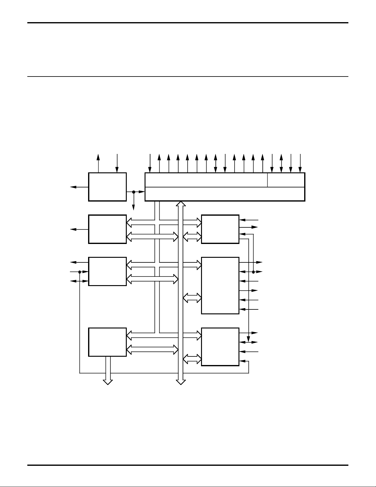
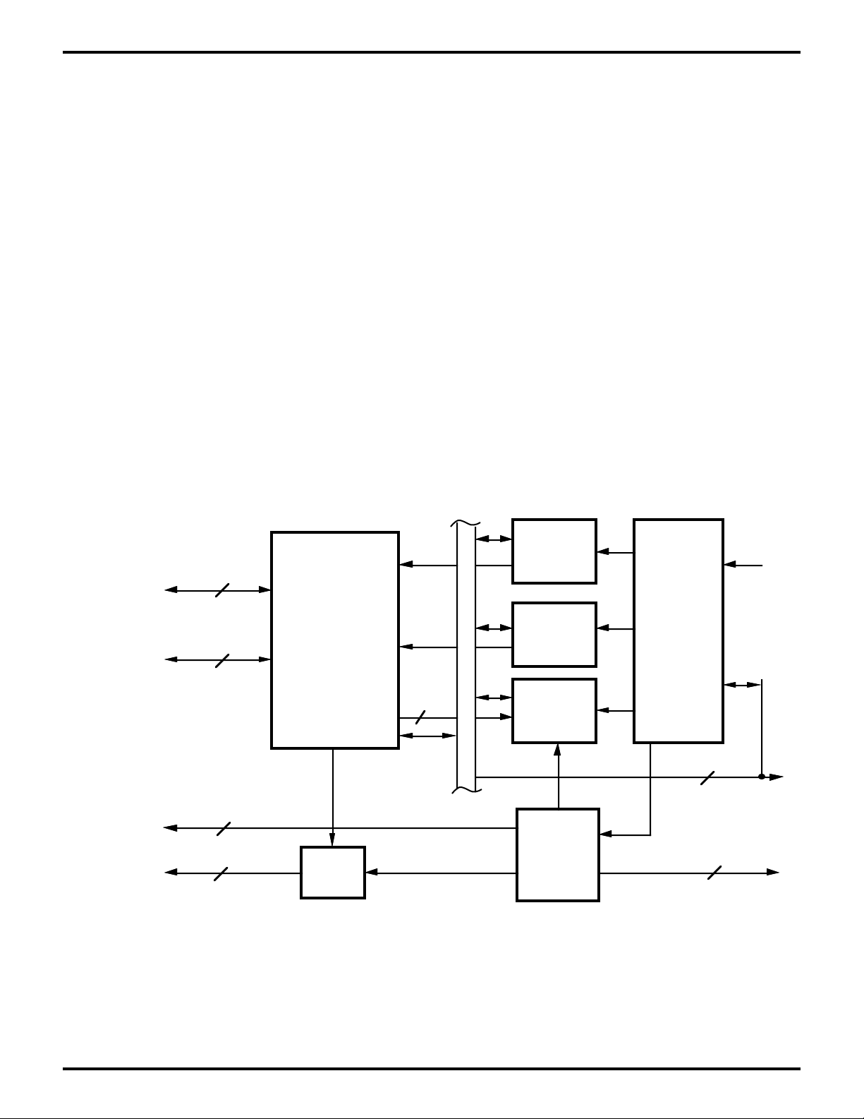
Z80182/Z8L182 FUNCTIONAL DESCRIPTION
ZILOG INTELLIGENT PERIPHERAL
Z80182/Z8L182
Functionally, the on-chip Z182 MPU and ESCC™ are the
same as the discrete devices (Figure 1). Therefore, for a
detailed description of each individual unit, refer to the
Z182 MPU FUNCTIONAL DESCRIPTION
This unit provides all the capabilities and pins of the Zilog
Z8S180 MPU (Static Z80180 MPU). Figure 4 shows the
S180 MPU Block Diagram of the Z182. This allows 100%
/WR
/RD
/RESET
A18
/TOUT
XTAL
Timing &
Ø
Generator
Programmable
Reload Timers
EXTAL
Clock
16-Bit
(2)
Product Specification/Technical Manuals of each discrete
product. The following subsections describe each of the
individual units of the Z182.
software compatibility with existing Z180™ (and Z80®)
software. The following is an overview of the major functional
units of the Z182.
/RFSH
/BUSACK
/BUSREQ
/WAIT
/HALT
/IORQ
/MREQ
/M1
Bus State Control Interrupt
CPU
DMACs
(2)
ST
/DREQ1
/TEND
/NMI
E
/INT0
/INT1
/INT2
TxS
RxS//CTS
CKS
Clocked
Serial I/O
Port
Data Bus (8-Bit)
Address Bus (16-Bit)
MMU
A19-A0 D7-D0
Figure 4. S180 MPU Block Diagram of Z182
Asynchronous
SCI
(Channel 0)
Asynchronous
SCI
(Channel 1)
TxA0
CKA0 /DREQ0
RxA0
/RTS0
/CTS0
/DCD0
TxA1
CKA1 /TEND0
RxA1
3-16
DS971820600
Page 17

Zilog
PRELIMINARY
ZILOG INTELLIGENT PERIPHERAL
Z80182/Z8L182
Z182 CPU
The Z182 CPU is 100% software compatible with the Z80
CPU and has the following additional features:
Faster Execution Speed. The Z182 CPU is “fine tuned,”
making execution speed, on average, 10% to 20% faster
than the Z80 CPU.
Enhanced DRAM Refresh Circuit. Z182 CPU’s DRAM
refresh circuit does periodic refresh and generates an
8-bit refresh address. It can be disabled or the refresh
period adjusted, through software control.
Enhanced Instruction Set. The Z182 CPU has seven
additional instructions to those of the Z80 CPU, which
include the MLT (Multiply) instruction.
HALT and Low Power Modes of Operation. The Z182
CPU has HALT and Low Power modes of operation, which
are ideal for the applications requiring low power
consumption like battery operated portable terminals.
System Stop Mode. When the Z182 is in System Stop
mode, it is only the Z180 MPU that is in STOP mode.
Standby and Idle Mode. Please refer to the Z8S180
Product Specification for additional information on these
two additional Low Power modes.
Instruction Set. The instruction set of the Z182 CPU is
identical to the Z180. For more details about each
transaction, please refer to the Product Specification/
Technical Manual for the Z180/Z80 CPU.
Z182 CPU Basic Operation
Z182 CPU’s basic operation consists of the following
events. These are identical to the Z180 MPU. For more
details about each operation, please refer to the Product
Specification/Technical Manual for the Z180.
■ Operation Code Fetch Cycle
■ Memory Read/Write Operation
■ Input/Output Operation
■ Bus Request/Acknowledge Operation
■ Maskable Interrupt Request Operation
Memory Management Unit (MMU)
®
The Memory Management Unit (MMU) allows the user to
map the memory used by the CPU (64 Kbytes of logical
addressing space) into 1 Mbyte of physical addressing
space. The organization of the MMU allows object code
compatibility with the Z80 CPU while offering access to an
extended memory space. This is accomplished by using
an effective common area-banked area scheme.
DMA Controller
The Z182 MPU has two DMA controllers. Each DMA
controller provides high-speed data transfers between
memory and I/O devices. Transfer operations supported
are memory-to-memory, memory-to/from-I/O, and I/O-toI/O. Transfer modes supported are request, burst, and
cycle steal. The DMA can access the full 1 Mbytes
addressing range with a block length up to 64 Kbytes and
can cross over 64K boundaries.
Asynchronous Serial Communication Interface
(ASCI)
This unit provides two individual full-duplex UARTs. Each
channel includes a programmable baud rate generator
and modem control signals. The ASCI channels also
support a multiprocessor communication format.
Programmable Reload Timer (PRT)
The Z182 MPU has two separate Programmable Reload
Timers, each containing a 16-bit counter (timer) and count
reload register. The time base for the counters is system
clock divided by 20. PRT channel 1 provides an optional
output to allow for waveform generation.
Clocked Serial I/O (CSI/O)
The CSI/O channel provides a half-duplex serial transmitter
and receiver. This channel can be used for simple highspeed data connection to another CPU or MPU.
Programmable Wait State Generator
To ease interfacing with slow memory and I/O devices, the
Z182 MPU unit has a programmable wait state generator.
By programming the DMA/WAIT Control Register (DCNTL),
up to three wait states are automatically inserted in memory
and I/O cycles. This unit also inserts wait states during onchip DMA transactions. When using RAMCS and ROMCS
wait state generators, the wait state controller with the
most programmed wait states will determine the number of
wait states inserted.
■ Trap and Non-Maskable Interrupt Request Operation
■ HALT and Low Power Modes of Operation
■ Reset Operation
DS971820600
3-17
Page 18

PRELIMINARYZilog
Z85230 ESCC™ FUNCTIONAL DESCRIPTION
ZILOG INTELLIGENT PERIPHERAL
Z80182/Z8L182
The Zilog Enhanced Serial Communication Controller
ESCC™ is a dual channel, multiprotocol data communication
peripheral. The ESCC functions as a serial-to-parallel,
parallel-to-serial converter/controller. The ESCC can be
software-configured to satisfy a wide variety of serial
communications applications. The device contains a variety
of new, sophisticated internal functions including on-chip
baud rate generators, digital phase-lock loops, and crystal
oscillators, which dramatically reduce the need for external
logic.
The ESCC handles asynchronous formats, synchronous
byte-oriented protocols such as IBM® Bisync, and
synchronous bit-oriented protocols such as HDLC and
IBM SDLC. This versatile device supports virtually any
serial data transfer application (telecommunication, LAN,
etc.)
The device can generate and check CRC codes in any
synchronous mode and can be programmed to check
data integrity in various modes. The ESCC also has facilities
for modem control in both channels in applications where
these controls are not needed, the modem controls can be
used for general-purpose I/O.
With access to 14 Write registers and 7 Read registers per
channel (number of the registers varies depending on the
version), the user can configure the ESCC to handle all
synchronous formats regardless of data size, number of
stop bits, or parity requirements. The ESCC also
accommodates all synchronous formats including
character, byte, and bit-oriented protocols.
The ESCC (Enhanced SCC) is pin and software compatible
to the CMOS SCC version. The following enhancements
were made to the CMOS SCC:
■ Deeper Transmit FIFO (4 bytes)
■ Deeper Receive FIFO (8 bytes)
■ Programmable FIFO interrupt and DMA request level
■ Seven enhancements to improve SDLC link layer
supports:
- Automatic transmission of the opening flag
- Automatic reset of Tx Underrun/EOM latch
- Deactivation of /RTS pin after closing flag
- Automatic CRC generator preset
- Complete CRC reception
- TxD pin automatically forced High with NRZI
encoding when using mark idle
- Status FIFO handles better frames with an ABORT
- Receive FIFO automatically unlocked for special
receive interrupts when using the SDLC status FIFO
■ Delayed bus latching for easier microprocessor
interface
■ New programmable features added with Write Register
7' (WR seven prime)
■ Write registers, 3, 4, 5 and 10 are now readable
■ Read register 0 latched during access
Within each operating mode, the ESCC also allows for
protocol variations by checking odd or even parity bits,
character insertion or deletion, CRC generation, checking
break and abort generation and detection, and many other
protocol-dependent features.
■ DPLL counter output available as jitter-free transmitter
clock source
■ Enhanced /DTR, /RTS deactivation timing
3-18
DS971820600
Page 19

Zilog
PRELIMINARY
ZILOG INTELLIGENT PERIPHERAL
Z80182/Z8L182
The following features are common to both the ESCC and
the CMOS SCC:
■ Two independent full-duplex channels
■ Synchronous/Isochronous data rates:
- Up to 1/4 of the PCLK using external clock source
- Up to 5 Mbits/sec at 20 MHz PCLK (ESCC).
■ Asynchronous capabilities
- 5, 6, 7 or 8 bits/character (capable of handling
4 bits/character or less)
- 1, 1.5, or 2 stop bits
- Odd or even parity
- Times 1, 16, 32 or 64 clock modes
- Break generation and detection
- Parity, overrun and framing error detection
■ Byte oriented synchronous capabilities:
- Internal or external character synchronization
- One or two sync characters (6 or 8 bits/sync
character) in separate registers
- Automatic Cyclic Redundancy Check (CRC)
generation/detection
■ NRZ, NRZI or FM encoding/decoding. Manchester
Code Decoding (Encoding with External Logic).
■ Baud Rate Generator in each Channel
■ Digital Phase-Locked Loop (DPLL) for Clock Recovery
■ Crystal Oscillator
The following features are implemented in the ESCC™ for
the Z80182/Z8L182 only:
■ New 32-bit CRC-32 (Ethernet Polynomial)
■ ESCC Programmable Clock
- programmed to be equal to system clock
divided by one or two
- programmed by Z80182 Enhancement Register
Note: The ESCC™ programmable clock must be
programmed to divide-by-two mode when operating above
the following conditions:
– PHI > 20 MHz at 5.0V
■ SDLC/HDLC capabilities:
- Abort sequence generation and checking
- Automatic zero insertion and detection
- Automatic flag insertion between messages
- Address field recognition
- I-field residue handling
- CRC generation/detection
- SDLC loop mode with EOP recognition/loop entry
and exit
– PHI > 10 MHz at 3.0V
DS971820600
3-19
Page 20
PRELIMINARYZilog
R
er
T
X
D
C
P
d
B
te
or
l
O
or
er
R
X
,
&
S
er
S
O
E
w
I
al
ol
C
A
r
C
B
r
I
pt
l
A
B
ce
D
us
C
ol
T
K
EIIEO
pt
ol
ZILOG INTELLIGENT PERIPHERAL
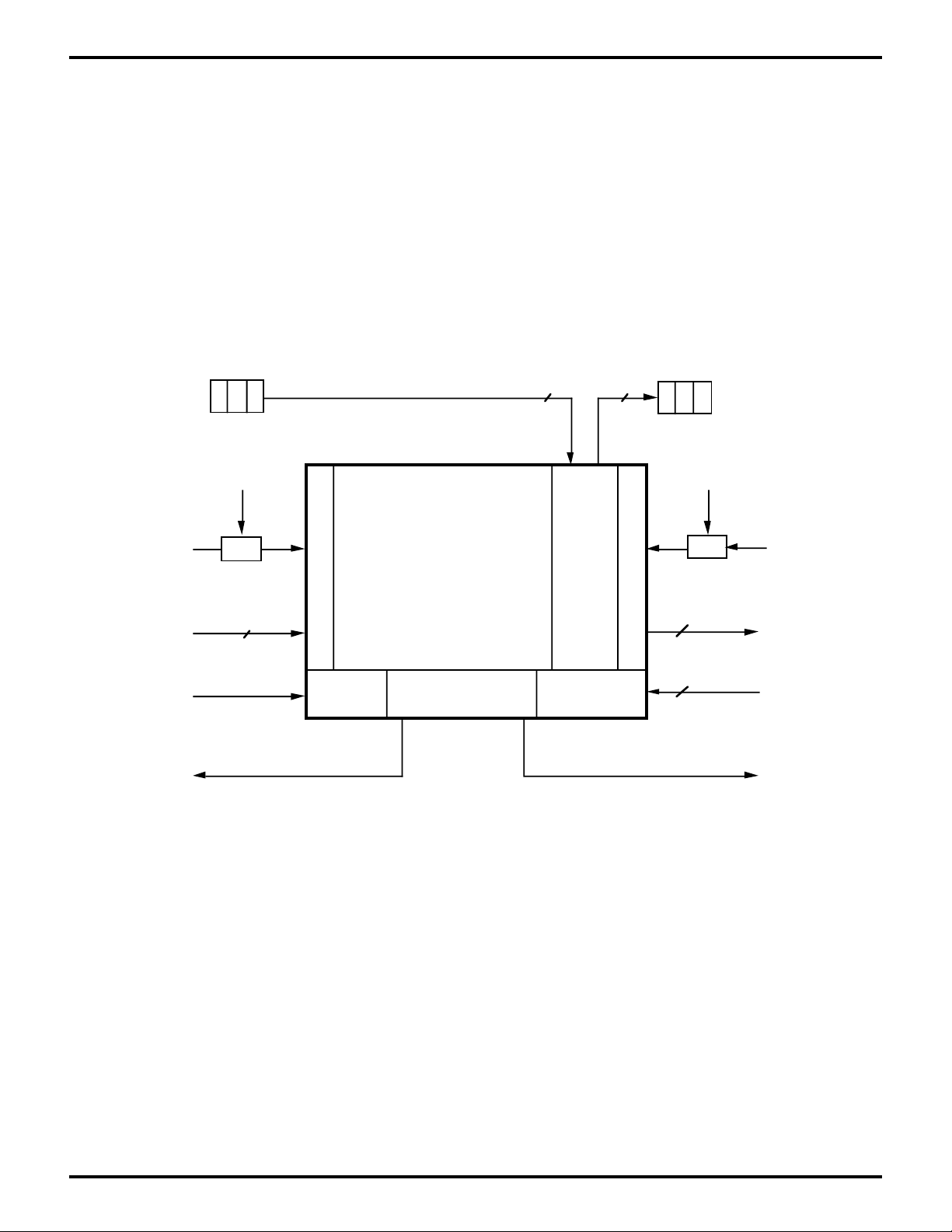
Z85230 ESCC™ BLOCK DIAGRAM
For a detailed description of the Z85230 ESCC, refer to the ESCC Technical Manual. The following figure is the block
diagram of the discrete ESCC, which was integrated into the Z182. The /INT line is internally connected to "INTO of the
Z182.
Transmit Logic
Z80182/Z8L182
Transmit FIFO
4 Bytes
ransmit MU
ata Encoding & CR
Generation
TxDA
Channel A
xploded Vie
eceive and Transmit Clock Multipex
Digital
hase-Locke
Loop
Rec. Status*
FIFO
DLC Frame Status FIF
10 x 19
* 8 bytes each
aud Ra
Generat
Modem/Control Logic
Receive Logic
Rec. Data*
FIFO
Crysta
scillat
Amplifi
eceive MU
CRC Checker
Data Decode
ync Charact
Detection
/TRxCA
/RTxCA
/CTSA
/DCDA
/SYNCA
/RTSA
/DTRA//REQA
RxDA
atab
ontr
Interru
Contr
CPU & DM
us Interfa
/IN
/INTAC
I
ntern
Contr
Logic
nterru
Contro
Logic
hannel
Registe
hannel
Registe
Channel A
Channel B
Figure 5. ESCC Block Diagram
3-20
DS971820600
Page 21
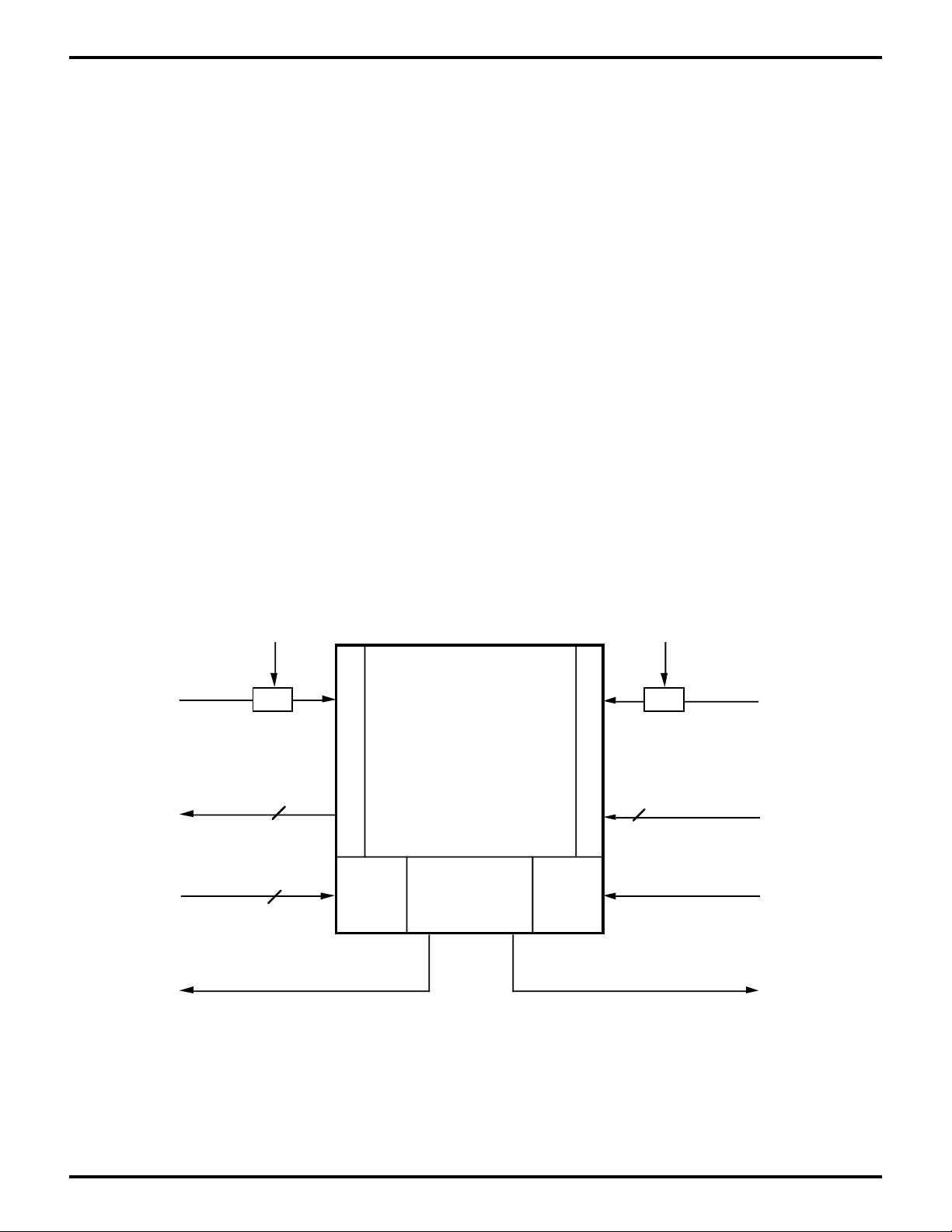
Zilog
PRELIMINARY
16550 MIMIC INTERFACE FUNCTIONAL DESCRIPTION
ZILOG INTELLIGENT PERIPHERAL
Z80182/Z8L182
The Z80182/Z8L182 has a 16550 MIMIC interface that
allows it to mimic the 16550 device. It has all the interface
pins necessary to connect to the PC/XT/AT bus. It contains
the complete register set of the part with the same interrupt
structure. The data path allows parallel transfer of data to
and from the register set by the internal Z80180 of the
Z80182/Z8L182. There is no shift register associated with
the mimic of the 16550 UART. This interface saves the
application from doing a serial transfer before performing
data compression or error correction on the data.
Control of the register set is maintained by six priority
encoded interrupts to the Z80182/Z8L182. When the PC/
XT/AT writes to THR, MCR, LCR, DLL, DLM, FCR or reads
the RBR, an interrupt to the Z80182/Z8L182 is generated.
Each interrupt can be individually masked off or all interrupts
can be disabled by writing a single bit. Both mode 0 and
mode 2 interrupts are supported by the 16550 MIMIC
interface.
16550 MIMIC Side
or PC Side Interface
Two eight-bit timers are also available to control the data
transfer rate of the 16550 MIMIC interface. Their input is
tied to the ESCC channel B divide clock, so a down count
of 24 bits is possible. An additional two eight bit timers are
available for programming the FIFO timeout feature (Four
Character Time Emulation) for both Receive and Transmit
FIFO’s.
The 16550 MIMIC interface supports the PC/XT/AT interrupt
structure as well as an additional mode that allows for a
wired Logic AND interrupt structure.
The 16550 MIMIC interface is also capable of high speed
parallel DMA transfers by using two control lines and the
transmit and receive registers of the 16550 MIMIC interface.
All registers of the 16550 MIMIC interface are accessible
in any page of I/O space since only the lowest eight
address lines are decoded. See Figure 6 for a block
diagram of the 16550 MIMIC interface.
MPU Side
Interface
PC
Addr/Decode
PC
Databus
PC DMA CNTL
PC IRQ
Receive
4
16550 MIMIC
8
2
1
Register Set
6
Databus
PC IRQ
Timer
Transmit
Timer
Z80180
IRQ
Control
DMA
Control
Control/
Config
Register
Z80180
Databus
Z80180
Address
8
2
Z80180
DMA
Control
DS971820600
Figure 6. 16550 MIMIC Block Diagram
3-21
Page 22
16550 MIMIC FIFO DESCRIPTION
PRELIMINARYZilog
ZILOG INTELLIGENT PERIPHERAL
Z80182/Z8L182
The receiver FIFO consists of a 16-word FIFO capable of
storing eight data bits and three error bits for each character
stored (Figure 7). Parity error, Framing error and Break
detect bits are stored along with the data bits by copying
their value from three shadow bits that are Write Only bits
for the Z80180 MPU LSR address. The three shadow bits
are cleared after they are copied to the FIFO memory. In
FIFO mode, to write error bits into the receiver FIFO, the
MPU must first write the Parity, Framing and Break detect
status to the Line Status Register (shadow bits) and then
write the character associated into the receiver buffer. The
data and error bits will then move into the same address in
MPU Write
LSR Shadow
B2-B4
MPU
CNTL
Line
MPU
Databus
(MPU Side Write)
Internal Clock
Internal Clock
Sync
8
W
R
I
T
E
B
U
F
F
E
R
Pointer
Write
16x8
Data Bits
ALU
the FIFO. The error bits become available to the PC side of
the interface when that particular location becomes the
next address to read (top of FIFO). At that time, they may
either be read by the PC by accessing them in the LSR, or
they may cause an interrupt to the PC interface if so
enabled. The error bits are set by the error status of the byte
at the top of the FIFO, but may only be cleared by reading
the LSR. If successive reads of the receiver FIFO are
performed without reading the LSR, the status bits will be
set if any of the bytes read have the respective error bit set.
See Table 6 for the setting and clearing of the Line Status
Register bits.
16x3
Error
Bits
Read
Pointer
error
3
R
E
A
D
B
U
F
F
E
R
Internal Clock
3
8
5
PC Read
LSR
B2-B4
PC
Cntrl
Line
Sync
PC Side
Databus
(PC Side Read)
FIFO Control
Register
3-22
MPU
IRQ
MPU Side
Interface
PC
IRQ
16550
MIMIC or
PC Side
Interface
Figure 7. 16550 MIMIC Receiver FIFO Block Diagram
DS971820600
Page 23

Zilog
PRELIMINARY
ZILOG INTELLIGENT PERIPHERAL
Table 6. 16550 Line Status Register
Error Description How to Set How to Clear
Error in At least one data byte available At least one error in receiver When there are no more
RCVR in FIFO with one error FIFO errors
FIFO
*TEMT Transmitter empty MPU writes a 1 MPU writes a 0
† *THRE Transmitter holding When MPU has When holding register
register is empty read or emptied is not empty
the holding register
Break Break occurs when MPU writes 1 There is a
Detect received data input PC-side read
is held in logic-0 of the LSR
for longer than a
full word transmission
Framing Received character MPU writes 1 There is a
Error did not have a valid PC-side read
stop bit of the LSR
Z80182/Z8L182
Parity Received character MPU writes 1 There is a
Error did not have correct PC-side read
even or odd parity of the LSR
Overrun Overlapping received MPU makes There is a
Error characters, thereby two writes PC-side read
destroying the to receiver of the LSR
previous character buffer register
†Data Indicates complete MPU writes to Empty Receiver
Ready incoming data has RCVR FIFO or or Receiver FIFO
been received receiver buffer
register
Notes:
* The TEMT and THRE bits take on different functions when
TEMT/Double Buffer mode is enabled.
† These signals are delayed to HOST when using character
emulation delay.
DS971820600
3-23
Page 24
PRELIMINARYZilog
16550 MIMIC FIFO DESCRIPTION (Continued)
ZILOG INTELLIGENT PERIPHERAL
Z80182/Z8L182
The PC interface may be interrupted when 1, 4, 8 or 14
bytes are available in the receiver FIFO by setting bits 6
and 7 in the FCR (FIFO Control Register, PC address 02H)
to the appropriate value. If the FIFO is not empty, but below
the above trigger value, a timeout interrupt is available if
the receiver FIFO is not written by the MPU or read by the
PC from an interval determined by the Character Timeout
Timer. This is an additional Timer with MPU access only
that is used to emulate the 16550 4 character timeout
delay.
The Receive FIFO timeout timers are designed to reload
and begin countdown after every read or write of the Rx
FIFO, regardless of the Rx trigger level or number of bytes
in the FIFO. Therefore, it is possible to get Timeout interrupts
more often than Receive data interrupts. In order to closely
emulate a 16550, a receive timeout timer enhancement is
provided. When enabling this feature, the timeout timer will
not begin counting down until the character emulation
timer for each byte of data in the Rx FIFO has expired.
Note: Enabling this feature will facilitate increased
16550 compatibility but may impede throughput.
If the
Receive Timeout interrupt occurs, the PC HOST will only
be allowed to read up to 4-5 consecutive characters
before the Data Ready bit is forced to zero (even if there
is still more data in FIFO). This is required to maintain
character pacing.
The timer receives the ESCC /TRxCB as its input clock.
Software must determine the correct values to program
into the Receiver Timeout register and the ESCC TRxCB to
achieve the correct delay interval for timeout. These
interrupts are cleared by the FIFO reaching the trigger
point or by resetting the Timeout Interval Timer by FIFO
MPU write or PC read access.
With FIFO mode enabled, the MPU is interrupted when the
receiver FIFO is empty, corresponding to bit 5 being set
in the IUS/IP register (MPU access only). This bit
corresponds to a PC read of the receive buffer in non-FIFO
(16450) mode. The interrupt source is cleared when the
FIFO becomes non-empty or the MPU reads the IUS/IP
register.
The transmitter FIFO is 16-byte FIFO with PC write and
MPU read access (Figure 8). In FIFO mode, the PC
receives an interrupt when the transmitter becomes empty
corresponding to bit 5 being set in the LSR. This bit and the
interrupt source are cleared when the transmit FIFO
becomes non-empty or the Interrupt Identification Register
(IIR) register is read by the PC.
MPU
CNTL
Line
MPU
Databus
(MPU Side Read)
FIFO
Control
Register
MPU
IRQ
MPU Side
Interface
Internal Clock
Sync
R
E
A
D
B
U
F
8
5
F
E
R
Read
Pointer
16x8
Data Bits
ALU
W
R
I
T
E
B
U
F
F
E
R
Write
Pointer
Figure 8. 16550 MIMIC Transmitter FIFO Block Diagram
Internal Clock
Sync
8
PC
Cntrl
Line
PC Side
Databus
(PC Side Write)
Internal
Clock
PC
IRQ
16550
MIMIC or
PC Side
Interface
3-24
DS971820600
Page 25

Zilog
PRELIMINARY
ZILOG INTELLIGENT PERIPHERAL
Z80182/Z8L182
On the MPU interface, the transmitted data available can
be programmed to interrupt the MPU on 1, 4, 8 or 14 bytes
of available data by seeing the appropriate value in the
MPU FSCR control register (MPU write only xxECH) bits 6
and 7. A timeout feature exists, Transmit Timeout Timer,
which is an additional 8-bit timer with SCC TxRCB as the
input source. If the transmitter FIFO is non-empty and no
PC write or MPU read of the FIFO has taken place within the
timer interval, a timeout occurs causing a corresponding
interrupt to the MPU.
Z80182/Z8L182 MIMIC SYNCHRONIZATION CONSIDERATIONS
Because of the asynchronous nature of the FIFO’s on the
MIMIC, some synchronization plan must be provided to
prevent conflict from the dual port accesses of the MPU
and the PC.
To solve this problem, I/O to the FIFO is buffered and the
buffers allow both PC and MPU to access the FIFO
asynchronously. Read and Write requests are then
synchronized by means of the MPU clock. Incoming signals
are buffered in such a way that metastable input levels are
stabilized to valid 1 or 0 levels. Actual transfers to and from
the buffers, from and to the FIFO memory, are timed by the
MPU clock. ALU evaluation is performed on a different
phase than the transfer to ensure stable pointer values.
Another potential problem is that of simultaneous access
of the MPU and PC to any of the various ‘mailbox’ type
registers. This is solved by dual buffering of the various
read/write registers. During a read access by either the
MPU or PC to a mailbox register, the data in the output or
slave portion of the buffered register is not permitted to
change. Any write that might take place during this time
will be stored in the input of master part of the register. The
corresponding status/interrupt is reset appropriately based
on the write having followed the read to the register. For
example, the IUS/IP bit for the LCR write will not be cleared
by the MPU read of the LCR if a simultaneous write to the
LCR by the PC takes place. Instead the LSR data will
change after the read access and IUS/IP bit 3 remains at
logic 1.
DS971820600
3-25
Page 26
PRELIMINARYZilog
Z80182 MIMIC DOUBLE BUFFERING FOR THE TRANSMITTER
ZILOG INTELLIGENT PERIPHERAL
Z80182/Z8L182
The Z80182 Rev DA implements double buffering for the
transmitter in 16450 mode and sets the TEMT bit in the LSR
Register automatically.
When this feature is enabled and character delay emulation
is being used (see Figure 9):
1. The PC THRE bit in the LSR Register is set when the
THR Register is empty;
2. PC Host writes to the 16450 THR Register;
3. Whenever the Z80182 TSR buffer is empty and one
character delay timer is in a timed-out state, the byte
from the THR Register is transferred to the TSR buffer;
the timer is in timed-out state after FIFO Reset or after
Host TEMT is set. This allows a dual write to THR when
Host TEMT is set.
4. Restart character delay timer (timer reloads and counts
down) with byte transfer from THR Register to the TSR
buffer;
5. Whenever the TSR buffer is full, the TEMT bit in MPU
LSR Register is reset with no delay;
6. MPU reads TSR buffer;
7. TEMT bit in LSR Register for MPU is set with no delay
whenever the TSR buffer is empty;
8. When the TSR buffer is read by MPU and THR Register
is empty and one character delay timer reaches zero,
the TEMT bit in the LSR Register for Host is set from 0
to 1.
The PC THRE bit in the LSR Register is reset whenever the
THR Register is full and set whenever THR Register is
empty.
MPU IREQ and DMA Request for the transmit data is
trigger whenever TSR buffer is full and cleared whenever
TSR buffer is empty.
If character delay emulation is not used the TEMT bit in the
LSR Register is set whenever both the THR Register and
the TSR buffer are both empty. The Host TEMT bit is clear
if there is data in either the TSR buffer of THR Register.
Host Write
Host & MPU THRE =
(MPU TEMT) TSRE =
Host TEMT = 1 if - THRE = 1
- TSRE = 1
- Emulation delay timer is timed out
Empty/Full
1 0
Empty/Full
1 0
16450
THR
Register
THR to TSR
delay
transfer
TSR
Transmit
Shift Reg.
Emulation
Byte Transfer if:
- THRE=0;
- TSR = 1;
- Character delay timer is timed out.
Note: Timer reloads and counts down
whenever data is transferred from THR to TSR.
Added TSR Buffer for the
transmit data
3-26
Note: MPU sees TSR bit in the LSR Register as TEMT bit
Figure 9. TEMT Emulation Logic Implementation
DS971820600
Page 27

Zilog
PRELIMINARY
PARALLEL PORTS FUNCTIONAL DESCRIPTION
ZILOG INTELLIGENT PERIPHERAL
Z80182/Z8L182
The Z80182/Z8L182 has three 8-bit bi-directional Ports.
Each bit is individually programmable for input or output
(with the exception of PC6 and PC7 which are inputs only).
The Ports are controlled through two registers: the Port
Direction Control Register and the Port Data Register.
(Please see register description for Ports A, B and C).
PROGRAMMING
The following subsections explain and define the
parameters for I/O Address assignments. The three tables
in this section describe the mapping of the common
registers shared by the MPU and the 16550 MIMIC. The
MPU address refers to the I/O address as accessed from
the MPU side (the Z180™ MPU interface side of the 16550
MIMIC). Note that only the lowest eight address lines are
decoded for Z182 peripheral access. The full sixteen
Table 7. Z80182/Z8L182 MPU Registers
Register Name MPU Addr PC Addr
Z80182/Z8L182 MPU Control Registers 0000H to 00x3FH None
Note:
“x” indicates don’t care condition
address lines are decoded for on-chip Z180 MPU access.
The PC address (coined because the UART is common in
PCs) is the address needed to access the MIMIC registers
through the MIMIC interface signals. The MIMIC interface
signals are multiplexed with the ESCC channel B and the
Port A signals, and must be activated through the System
Configuration Register and the Interrupt Edge/Pin MUX
Register.
(Relocatable to 0040H to 007FH
or 0080H to 00BFH)
Table 8. Z80182/Z8L182 MIMIC Register MAP
Register Name MPU Addr/Access PC Addr/Access
MMC MIMIC Master Control Register xxFFH R/W None
IUS/IP Interrupt Pending xxFEH R/Wb7 None
IE Interrupt Enable xxFDH R/W None
IVEC Interrupt Vector xxFCH R/W None
TTCR Transmit Time Constant xxFAH R/W None
RTCR Receive Time Constant xxFBH R/W None
FSCR FIFO Status and Control xxECH R/W7-4 None
RTTC Receive Timeout Time Constant xxEAH R/W None
TTTC Transmit Timeout Time Constant xxEBH R/W None
RBR Receive Buffer Register xxF0H W only 00H DLAB=0 R only
THR Transmit Holding Register xxF0H R only 00H DLAB=0 W only
IER Interrupt Enable Register xxF1H R only 01H DLAB=0 R/W
IIR Interrupt Identification None 02H R only
FCR FIFO Control Register xxE9H R only 02H W only
MM REGISTER XXE9H W only None
LCR Line Control Register xxF3H R only 03H R/W
MCR Modem Control Register xxF4H R only 04H R/W
LSR Line Status Register xxF5H R/Wb6432 05H R only
MSR Modem Status Register xxF6H R/Wb7-4 06H R only
SCR Scratch Register xxF7H R only 07H R/W
DLL Divisor Latch (LSByte) xxF8H R only 00H DLAB=1 R/W
DLM Divisor Latch (MSByte) xxF9H R only 01H DLAB=1 R/W
DS971820600
3-27
Page 28

PRELIMINARYZilog
ZILOG INTELLIGENT PERIPHERAL
PROGRAMMING (Continued)
Table 9. Z80182/Z8L182 ESCC, PIA and MISC Registers
Register Name MPU Addr/Access PC Addr/Access
WSG Chip Select Register xxD8H R/W None
Z80182 Enhancements Register xxD9H R/W None
PC Data Direction Register xxDDH R/W None
PC Data Register xxDEH R/W None
Interrupt Edge/Pin MUX Control xxDFH R/W None
ESCC Chan A Control Register xxE0H R/W None
ESCC Chan A Data Register xxE1H R/W None
ESCC Chan B Control Register xxE2H R/W None
ESCC Chan B Data Register xxE3H R/W None
PB Data Direction Register xxE4H R/W None
PB Data Register xxE5H R/W None
RAMUBR RAM Upper Boundary Register xxE6H R/W None
RAMLBR RAM Lower Boundary Register xxE7H R/W None
ROM Address Boundary Register xxE8H R/W None
PA Data Direction Register xxEDH R/W None
PA Data Register xxEEH R/W None
System Configuration Register xxEFH R/W None
Z80182/Z8L182
3-28
DS971820600
Page 29
Zilog
PRELIMINARY
Z182 MPU CONTROL REGISTERS
Figures 10 through 50 refer to the Z80182/Z8L182 MPU
Control registers. For additional information, refer to the
Z8S180 Product Specification and Technical Manual.
ASCI CHANNELS CONTROL REGISTERS
ZILOG INTELLIGENT PERIPHERAL
Z80182/Z8L182
Bit
Upon RESET
R/W
CNTLA0
MPE
R/W0R/W0R/W1R/WxR/W0R/W0R/W0R/W
RE TE /RTS0
0
MPBR/
MOD2 MOD1 MOD0
EFR
0 0 0 Start + 7-Bit Data + 1 Stop
0 0 1 Start + 7-Bit Data + 2 Stop
0 1 0 Start + 7-Bit Data + Parity + 1 Stop
0 1 1 Start + 7-Bit Data + Parity + 2 Stop
1 0 0 Start + 8-Bit Data + 1 Stop
1 0 1 Start + 8-Bit Data + 2 Stop
1 1 0 Start + 8-Bit Data + Parity + 1 Stop
1 1 1 Start + 8-Bit Data + Parity + 2 Stop
Addr 00H
Figure 10a. ASCI Control Register A (Ch. 0)
MODE Selection
Read - Multiprocessor Bit Receive
Write - Error Flag Reset
Request To Send
Transmit Enable
Receive Enable
Multiprocessor Enable
DS971820600
3-29
Page 30
PRELIMINARYZilog
ASCI CHANNELS CONTROL REGISTERS (Continued)
ZILOG INTELLIGENT PERIPHERAL
Z80182/Z8L182
Bit
Upon RESET
R/W
CNTLA1
MPBR/
MPE RE TE
0
R/W0R/W0R/W1R/WxR/W0R/W0R/W0R/W
CKA1D
MOD2 MOD1 MOD0
EFR
0 0 0 Start + 7-Bit Data + 1 Stop
0 0 1 Start + 7-Bit Data + 2 Stop
0 1 0 Start + 7-Bit Data + Parity + 1 Stop
0 1 1 Start + 7-Bit Data + Parity + 2 Stop
1 0 0 Start + 8-Bit Data + 1 Stop
1 0 1 Start + 8-Bit Data + 2 Stop
1 1 0 Start + 8-Bit Data + Parity + 1 Stop
1 1 1 Start + 8-Bit Data + Parity + 2 Stop
Addr 01H
Figure 10b. ASCI Control Register A (Ch. 1)
MODE Selection
Read - Multiprocessor Bit Receive
Write - Error Flag Reset
CKA1 Disable
Transmit Enable
Receive Enable
Multiprocessor Enable
3-30
DS971820600
Page 31

Zilog
PRELIMINARY
ZILOG INTELLIGENT PERIPHERAL
Z80182/Z8L182
Addr 02H
Clock Source and Speed Select
Divide Ratio
Parity Even or Odd
Clear To Send/Prescale
Multiprocessor
Multiprocessor Bit Transmit
Bit
Upon Reset
R/W
CNTLB0
MPBT MP
Invalid
R/W0R/W†R/W0R/W0R/W1R/W1R/W1R/W
† /CTS - Depending on the condition of /CTS pin.
PS - Cleared to 0.
/CTS/
PS
SS2 SS1 SS0
DRPE0
General PS = 0 PS = 1
Divide Ratio (Divide Ratio = 10) (Divide Ratio = 30)
SS, 2, 1, 0 DR = 0 (x16) DR = 1 (x64) DR = 0 (x16) DR = 1 (x64)
000 Ø ÷ 160 Ø ÷ 640 Ø ÷ 480 Ø ÷ 1920
001 Ø ÷ 320 Ø ÷ 1280 Ø ÷ 960 Ø ÷ 3840
010 Ø ÷ 640 Ø ÷ 2580 Ø ÷ 1920 Ø ÷ 7680
011 Ø ÷ 1280 Ø ÷ 5120 Ø ÷ 3840 Ø ÷ 15360
100 Ø ÷ 2560 Ø ÷ 10240 Ø ÷ 7680 Ø ÷ 30720
101 Ø ÷ 5120 Ø ÷ 20480 Ø ÷ 15360 Ø ÷ 61440
110 Ø ÷ 10240 Ø ÷ 40960 Ø ÷ 30720 Ø ÷ 122880
111 External Clock (Frequency < Ø ÷ 40)
Figure 11. ASCI Control Register B (Ch. 0)
DS971820600
3-31
Page 32

PRELIMINARYZilog
ASCI CHANNELS CONTROL REGISTERS (Continued)
ZILOG INTELLIGENT PERIPHERAL
Z80182/Z8L182
Addr 03H
Clock Source and Speed Select
Divide Ratio
Parity Even or Odd
Read - Status of /CTS pin
Write - Select PS
Multiprocessor
Multiprocessor Bit Transmit
Bit
Upon Reset
R/W
CNTLB1
MPBT MP
Invalid
R/W0R/W0R/W0R/W0R/W1R/W1R/W1R/W
/CTS/
PS
DRPE0
SS2 SS1 SS0
General PS = 0 PS = 1
Divide Ratio (Divide Ratio = 10) (Divide Ratio = 30)
SS, 2, 1, 0 DR = 0 (x16) DR = 1 (x64) DR = 0 (x16) DR = 1 (x64)
000 Ø ÷ 160 Ø ÷ 640 Ø ÷ 480 Ø ÷ 1920
001 Ø ÷ 320 Ø ÷ 1280 Ø ÷ 960 Ø ÷ 3840
010 Ø ÷ 640 Ø ÷ 2580 Ø ÷ 1920 Ø ÷ 7680
011 Ø ÷ 1280 Ø ÷ 5120 Ø ÷ 3840 Ø ÷ 15360
100 Ø ÷ 2560 Ø ÷ 10240 Ø ÷ 7680 Ø ÷ 30720
101 Ø ÷ 5120 Ø ÷ 20480 Ø ÷ 15360 Ø ÷ 61440
110 Ø ÷ 10240 Ø ÷ 40960 Ø ÷ 30720 Ø ÷ 122880
*111 External Clock (Frequency < Ø ÷ 40)
Note:
* Baud rate is external clock rate ÷16; therefore, Ø ÷(40 x 16)
is maximum baud rate using external clocking.
3-32
Figure 12. ASCI Control Register B (Ch. 1)
DS971820600
Page 33

Zilog
PRELIMINARY
ZILOG INTELLIGENT PERIPHERAL
Z80182/Z8L182
Bit
Upon Reset
R/W
STAT0
RDRF OVRN /DCD0 TDRE TIE
0R0R0
†† /CTS0 Pin TDRE
L 1
H 0
PE
R0R0R/W R††R0R/W
† /DCD0 - Depending on the condition of /DCD0 Pin.
RIEFE
†
Addr 04H
Figure 13. ASCI Status Register
Transmit Interrupt Enable
Transmit Data Register
Empty
Data Carrier Detect
Receive Interrupt Enable
Framing Error
Parity Error
Over Run Error
Receive Data Register Full
Upon Reset
R/W
STAT1
Bit
RDRF OVRN CTS1E TDRE TIE
0
R0R0R0R0R/W R/W1R0R/W
PE
RIEFE
0
Figure 14. ASCI Status Register (Ch. 1)
Addr 05H
Transmit Interrupt Enable
Transmit Data Register
Empty
/CTS1 Enable
Receive Interrupt Enable
Framing Error
Parity Error
Over Run Error
Receive Data Register Full
DS971820600
3-33
Page 34

PRELIMINARYZilog
ASCI CHANNELS CONTROL REGISTERS (Continued)
ZILOG INTELLIGENT PERIPHERAL
Z80182/Z8L182
TDR0
Write Only Addr 06H
76543210
Transmit Data
Figure 15. ASCI Transmit Data Register (Ch. 0)
TDR1
Write Only
Addr 07H
76543210
Transmit Data
Figure 16. ASCI Transmit Data Register (Ch. 1)
TSR0
Read Only
Addr 08H
xxxxxxxx
Received Data
Figure 17. ASCI Receive Data Register (Ch. 0)
TSR1
Read Only Addr 09H
xxxxxxxx
Received Data
Figure 18. ASCI Receive Data Register (Ch. 1)
BRK0
Read/Write
76543210
Addr 12H
Break generate bit
0 = no break
1 = break
Break detect bit
0 = no break
1 = break
Break feature bit
0 = dissolve
1 = enable
Figure 19. ASCI Break Control Register (Ch. 0)
BRK1
Read/Write
76543210
Addr 13H
Break generate bit
0 = no break
1 = break
Break detect bit
0 = no break
1 = break
Break feature enable bit
0 = disable
1 = enable
Figure 20. ASCI Break Control Register (Ch. 1)
3-34
DS971820600
Page 35

Zilog
CSI/O REGISTERS
PRELIMINARY
ZILOG INTELLIGENT PERIPHERAL
Z80182/Z8L182
CNTR
Bit
EF EIE SS2 SS1 SS0
Upon Reset
R/W
0
R0R/W0R/W0R/W
SS2, 1, 0 Baud Rate
000 Ø ÷ 20
001 Ø ÷ 40
010 Ø ÷ 80
011 Ø ÷ 100
Figure 21. CSI/O Control Register
RE
Addr 0AH
-TE
11
R/W1R/W1R/W
Speed Select
Transmit Enable
Receive Enable
End Interrupt Enable
End Flag
SS2, 1, 0 Baud Rate
100 Ø ÷ 320
101 Ø ÷ 640
110 Ø ÷ 1280
111 External Clock
(Frequency < Ø ÷ 20)
TRDR
Read/Write Addr 0BH
76543210
Read - Received Data
Write - Transmit Data
Figure 22. CSI/O Transmit/Receive Data Register
DS971820600
3-35
Page 36

TIMER DATA REGISTERS
PRELIMINARYZilog
ZILOG INTELLIGENT PERIPHERAL
Z80182/Z8L182
TMDR0L
Read/Write Addr 0CH
76543210
Figure 23. Timer 0 Data Register L
TMDR1L
Read/Write
76543210
Addr 14H
Figure 24. Timer 1 Data Register L
TIMER RELOAD REGISTERS
RLDR0L
Read/Write
76543210
Addr 0EH
TMDR0H
Read/Write Addr 0DH
15 14 13 12 11 10 9 8
When Read, read Data Register L
before reading Data Register H.
Figure 25. Timer 0 Data Register H
TMDR1H
Read/Write Addr 15H
15 14 13 12 11 10 9 8
When Read, read Data Register L
before reading Data Register H.
Figure 26. Timer 1 Data Register H
RLDR0H
Read/Write
15 14 13 12 11 10 9 8
Addr 0FH
Figure 27. Timer 0 Reload Register L
RLDR1L
Read/Write
76543210
Addr 16H
Figure 28. Timer 1 Reload Register L
Figure 29. Timer 0 Reload Register H
RLDR1H
Read/Write
15 14 13 12 11 10 9 8
Addr 17H
Figure 30. Timer 1 Reload Register H
3-36
DS971820600
Page 37

Zilog
TIMER CONTROL REGISTER
PRELIMINARY
ZILOG INTELLIGENT PERIPHERAL
Z80182/Z8L182
Bit
Upon Reset
R/W
TCR
TIF1 TIF0 TOC0 TDE1 TDE0
0
R
TOC1,0 A15/TOUT
00 Inhibited
01 Toggle
10 0
11 1
TIE1
0
R0R/W0R/W0R/W R/W0R/W0R/W
TOC1TIE0
Addr 10H
0
Figure 31. Timer Control Register
Timer Down Count Enable 1,0
Timer Output Control 1,0
Timer Interrupt Enable 1,0
Timer Interrupt Flag 1,0
DS971820600
3-37
Page 38

FREE RUNNING COUNTER
CPU CONTROL REGISTER
PRELIMINARYZilog
FRC
Read Only Addr 18H
76543210
Figure 32. Free Running Counter
ZILOG INTELLIGENT PERIPHERAL
Z80182/Z8L182
DMA REGISTERS
CPU Control Register (CCR)
D7 D6 D5 D4D3 D2 D1 D0
00000000
Addr 1FH
Figure 33. CPU
Note: See Figure 49 for full description.
SAR0L
Read/Write Addr 20H
SA7 SA0
SAR0H
Read/Write Addr 21H
SA15 SA8
SAR0B
Read/Write Addr 22H
SA16SA19
----
3-38
Bits 0-2 (3) are used for SAR0B
A19,
A18,
A17,
A16
DMA Transfer Request
x
x
0
0
x
x
x
x
0
x
1
x
1
/DREQ0 (external)
1
RDR0 (ASCI0)
0
RDR1 (ASCI1)
1
Not Used
Figure 34. DMA 0 Source Address Registers
DS971820600
Page 39

Zilog
DMA REGISTERS
DAR0L
Read/Write Addr 23H
DA7 DA0
PRELIMINARY
MAR1L
Read/Write
MA7 MA0
ZILOG INTELLIGENT PERIPHERAL
Z80182/Z8L182
Addr 28H
DAR0H
Read/Write Addr 24H
DA15 DA8
DAR0B
Read/Write Addr 25H
DA16DA19
----
Bits 0-2 (3) are used for DAR0B
A19,
A18,
A17,
A16
x
x
x
x
x
0
x
0
x
1
x
1
DMA Transfer Request
0
/DREQ0 (external)
1
TDR0 (ASCI0)
0
TDR1 (ASCI1)
1
Not Used
Figure 35. DMA 0 Destination Address Registers
BCR0L
Read/Write
BC7 BC0
Addr 26H
MAR1H
Read/Write
MA15 MA8
MAR1B
Read/Write
----
Addr 29H
Addr 2AH
MA16MA19
Figure 37. DMA 1 Memory Address Registers
IAR1L
Read/Write
IA7 IA0
IAR1H
Read/Write
IA15 IA8
Addr 2BH
Addr 2CH
BCR0H
Read/Write
BC15 BC8
Addr 27H
Figure 36. DMA 0 Byte Counter Registers
Figure 38. DMA I/O Address Registers
BCR1L
Read/Write
BC7 BC0
BCR1H
Read/Write
BC15 BC8
Addr 2EH
Addr 2FH
Figure 39. DMA 1 Byte Count Registers
DS971820600
3-39
Page 40

DMA REGISTERS (Continued)
PRELIMINARYZilog
ZILOG INTELLIGENT PERIPHERAL
Z80182/Z8L182
Bit
Upon Reset
Bit
Upon Reset
R/W
DSTAT
DE1 DE0 DIE0
0
R/W0R/W1W1W
/DWE1
DIE1/DWE0
00
R/W
Figure 40. DMA Status Register
DMODE
- -
110
DM1
R/W0R/W
SM1DM0
00
R/W R/W
10
R/W
SM0 MMOD
01
R/W
Addr 30H
DIME
RR/W
DMA Master Enable
DMA Interrupt Enable 1, 0
DMA Enable Bit Write Enable 1, 0
DMA Enable Ch 1, 0
Addr 31H
-
Memory MODE Select
Ch 0 Source Mode 1, 0
Ch 0 Destination Mode 1, 0
DM1, 0
00
01
10
11
MMOD
0
1
Destination
M
M
M
I/O
Mode
Cycle Steal Mode
Burst Mode
Address
DAR0+1
DAR0-1
DAR0 Fixed
DAR0 Fixed
SM1, 0
00
01
10
11
Source
M
M
M
I/O
SAR0 Fixed
SAR0 Fixed
Figure 41. DMA Mode Registers
Address
SAR0+1
SAR0-1
3-40
DS971820600
Page 41

Zilog
PRELIMINARY
ZILOG INTELLIGENT PERIPHERAL
Z80182/Z8L182
Bit
Upon Reset
R/W
DCNTL
MWI1 MWI0 DMS0 DIM1 DIM0
111
*
MWI1, 0
00
01
10
11
DMSi
1
0
IWI1
R/W1R/W
No. of Wait States
0
1
2
3
Sense
Edge Sense
Level Sense
DMS1IWI0
00
R/W R/WR/WR/W R/W
R/W
IWI1, 0
00
01
10
11
00
No. of Wait States
Addr 32H
DMA Ch 1 I/O Memory
Mode Select
/DREQi Select, i = 1, 0
I/0 Wait Insertion
Memory Wait Insertion
1
2
3
4
DM1, 0
00
01
10
11
Note:
* If using ROM/RAM Chip Select wait state generators,
the Z180 wait state generator should be set to 0.
Transfer Mode
M - I/O
M - I/O
I/O - M
I/O - M
Address Increment/Decrement
MAR1+1
MAR1-1
IAR1 Fixed
IAR1 Fixed
Figure 42. DMA/WAIT Control Register
IAR1 Fixed
IAR1 Fixed
MAR1+1
MAR1-1
DS971820600
3-41
Page 42

MMU REGISTERS
PRELIMINARYZilog
ZILOG INTELLIGENT PERIPHERAL
Z80182/Z8L182
Upon Reset
R/W
Bit
Upon Reset
R/W
CBR
CB7 CB6 CB2 CB1 CB0
Bit
000
R/W0R/W
CB3CB4CB5
00
R/W
R/W R/WR/WR/W R/W
Figure 43. MMU Common Base Register
BBR
BB7
BB6 BB2 BB1 BB0
000
R/W0R/W
BB3BB4BB5
00
R/W R/WR/WR/W R/W
R/W
Figure 44. MMU Bank Base Register
Addr 38H
00
MMU Common Base
Register
Addr 39H
00
MMU Bank Base Register
Bit
Upon Reset
R/W
CBAR
CA3 CA2 BA2 BA1 BA0
111
R/W1R/W
BA3CA0CA1
00
R/W R/WR/WR/W R/W
R/W
Addr 3AH
00
Figure 45. MMU Common/Bank Area Register
MMU Bank Area Register
MMU Common Area Register
3-42
DS971820600
Page 43

Zilog
SYSTEM CONTROL REGISTERS
PRELIMINARY
ZILOG INTELLIGENT PERIPHERAL
Z80182/Z8L182
Bit
Upon Reset
R/W
Upon Reset
R/W
Bit
IL
IL7 IL6 - - -
000
R/W
R/WR/W
Figure 46. Interrupt Vector Low Register
ITC
TRAP UFO ITE2 ITE1 ITE0
001
00000
--IL5
---
110
R/W
Addr 33H
Addr 34H
01
R/WRR/W R/W
Interrupt Vector Low
/INT Enable 2, 1, 0
Undefined Fetch Object
TRAP
Bit
Upon Reset
R/W
Figure 47. INT/TRAP Control Register
RCR
REFE REFW
111
CYC1, 0
00
01
10
11
Interval of Refresh Cycle
11100
10 states
20 states
40 states
80 states
--
-
CYC1 CYC0
R/WR/WR/W R/W
Addr 36H
Cycle Select
Refresh Wait State
Refresh Enable
DS971820600
Figure 48. Refresh Control Register
3-43
Page 44

PRELIMINARYZilog
SYSTEM CONTROL REGISTERS (Continued)
ZILOG INTELLIGENT PERIPHERAL
Z80182/Z8L182
Bit
Upon Reset
R/W
Bit
Upon Reset
R/W
OMCR
M1E /M1TE
111
Note:
This register should be programmed to 0x0xxxxxb
(x = don't care) as a part of Initialization.
/IOC
WR/W R/W
--
11111
Addr 3EH
---
Figure 49. Operation Mode Control Register
ICR
IOA7 IOA6
000
IOSTP
R/WR/W R/W
--
11111
Addr 3FH
---
I/O Compatibility
/M1 Temporary Enable
/M1 Enable
I/O Stop
I/O Address
Combination of 11
is reserved
Figure 50. I/O Control Register
3-44
DS971820600
Page 45

Zilog
PRELIMINARY
ADDITIONAL FEATURES ON THE Z182 MPU
ZILOG INTELLIGENT PERIPHERAL
Z80182/Z8L182
The following is a detailed description of the enhancements
to the Z8S180 from the standard Z80180 in the areas of
STANDBY, IDLE, and STANDBY-QUICK RECOVERY
modes.
I/Os are still operating. In I/O STOP mode, the on-chip I/Os
are in a stopped state while leaving the CPU running. In
SYSTEM STOP mode, both the CPU and the on-chip I/Os
are in the stopped state to reduce the current consumption.
The Z8S180 has added two additional power-down modes,
Add-On Features
There are five different power-down modes. SLEEP and
SYSTEM STOP are inherited from the Z80180. In SLEEP
STANDBY and IDLE, to reduce the current consumption
even further. The differences among these power-down
modes are summarized in Table 10.
mode, the CPU is in a stopped state while the on-chip
Table 10. Power Down Modes
Power-Down CPU On-Chip Recovery Recovery Time
Modes Core I/O OSC. CLKOUT Source (Minimum)
SLEEP Stop Running Running Running RESET, Interrupts 1.5 Clock
I/O STOP Running Stop Running Running By Programming SYSTEM STOP Stop Stop Running Running RESET, Interrupts 1.5 Clock
†
IDLE
STANDBY
†
Stop Stop Running Stop RESET, Interrupts, BUSREQ 8 +1.5 Clock
Stop Stop Stop Stop RESET, Interrupts, BUSREQ 217 +1.5 Clock (Normal Recovery)
26 +1.5 Clock (Quick Recovery)
Notes:
†
IDLE and STANDBY modes are only offered in Z8S180. Note that the
minimum recovery time can be achieved if INTERRUPT is used as the
Recovery Source.
STANDBY Mode
The Z8S180 has been designed to save power. Two lowpower programmable power-down modes have been
added; STANDBY mode and IDLE mode. The
STANDBY/IDLE mode is selected by multiplexing D6 and
D3 of the CPU Control Register (CCR, I/O Address = 1FH).
To enter STANDBY mode:
1. Set D6 and D3 to 1 and 0, respectively.
2. Set the I/O STOP bit (D5 of ICR,
I/O Address = 3FH) to 1.
3. Execute the SLEEP instruction.
When the part is in STANDBY mode, it behaves similar to
the SYSTEM STOP mode which currently exists on the
Z80180, except that the STANDBY mode stops the external
oscillator, internal clocks and reduces power consumption
to typically 50 µA..
Since the clock oscillator has been stopped, a restart of
the oscillator requires a period of time for stabilization. An
18-bit counter has been added in the Z8S180 to allow for
oscillator stabilization. When the part receives an external
IRQ or BUSREQ during STANDBY mode, the oscillator is
restarted and the timer counts down 217 counts before
acknowledgment is sent to the interrupt source.
The recovery source needs to remain asserted for duration
of the 217 count, otherwise standby will be resumed.
The following is a description of how the part exits STANDBY
for different interrupts and modes of operation.
STANDBY Mode Exit with /RESET
The /RESET input needs to be asserted for a duration long
enough for the crystal oscillator to stabilize and then exit
from the STANDBY mode. When /RESET is de-asserted, it
goes through the normal reset timing to start instruction
execution at address (logical and physical) 0000H.
The clocking is resumed within the Z8S180 and at the
system clock output after /RESET is asserted when the
crystal oscillator is restarted, but not yet stabilized.
DS971820600
3-45
Page 46

PRELIMINARYZilog
ZILOG INTELLIGENT PERIPHERAL
Z80182/Z8L182
STANDBY Mode Exit with BUS REQUEST
Optionally, if the BREXT bit (D5 of CPU Control Register)
is set to 1, the Z8S180 exits STANDBY mode when the
/BUSREQ input is asserted; the crystal oscillator is then
restarted. An internal counter automatically provides time
for the oscillator to stabilize, before the internal clocking
and the system clock output of the Z8S180 are resumed.
The Z8S180 relinquishes the system bus after the clocking
is resumed by:
- Tri-State the address outputs A19 through A0.
- Tri-State the bus control outputs /MREQ, /IORQ,
/RD and /WR.
- Asserting /BUSACK
The Z8S180 regains the system bus when /BUSREQ is
deactivated. The address outputs and the bus control
outputs are then driven High; the STANDBY mode is
exited.
If the BREXT bit of the CPU Control Register (CCR) is
cleared, asserting the /BUSREQ would not cause the
Z8S180 to exit STANDBY mode.
If STANDBY mode is exited due to a reset or an external
interrupt, the Z8S180 remains relinquished from the system
bus as long as /BUSREQ is active.
If an External Maskable Interrupt input is asserted, the CPU
responds according to the status of the Global Interrupt
Enable Flag IEF1 (determined by the ITE1 bit) and the
settings of the corresponding interrupt enable bit in the
Interrupt/Trap Control Register (ITC: I/O Address = 34H):
a. If an interrupt source is disabled in the ITC, asserting
the corresponding interrupt input would not cause the
Z8S180 to exit STANDBY mode. This is true regardless
of the state of the Global Interrupt Enable Flag IEF1.
b. If the Global Interrupt Flag IEF1 is set to 1, and if an
interrupt source is enabled in the ITC, asserting the
corresponding interrupt input causes the Z8S180 to
exit STANDBY mode. The CPU performs an interrupt
acknowledge sequence appropriate to the input being
asserted when clocking is resumed if:
- The interrupt input follows the normal interrupt
daisy chain protocol.
- The interrupt source is active until the acknowledge
cycle is completed.
c. If the Global Interrupt Flag IEF1 is disabled, i.e., reset
to 0, and if an interrupt source is enabled in the ITC,
asserting the corresponding interrupt input will still
cause the Z8S180 to exit STANDBY mode. The CPU
will proceed to fetch and execute instructions that
follow the SLEEP instruction when clocking is resumed.
STANDBY Mode Exit with External
Interrupts
STANDBY mode can be exited by asserting input /NMI.
The STANDBY mode may also exit by asserting /INT0,
/INT1 or /INT2, depending on the conditions specified in
the following paragraphs.
/INT0 wake-up requires assertion throughout duration of
clock stabilization time (2
If exit conditions are met, the internal counter provides
time for the crystal oscillator to stabilize, before the internal
clocking and the system clock output within the Z8S180
are resumed.
1. Exit with Non-Maskable Interrupts
If /NMI is asserted, the CPU begins a normal NMI interrupt
acknowledge sequence after clocking resumes.
2. Exit with External Maskable Interrupts
17
clocks).
If the External Maskable Interrupt input is not active until
clocking resumes, the Z8S180 will not exit STANDBY
mode. If the Non-Maskable Interrupt (/NMI) is not active
until clocking resumes, the Z8S180 still exits the STANDBY
mode even if the interrupt sources go away before the
timer times out, because /NMI is edge-triggered. The
condition is latched internally once /NMI is asserted Low.
IDLE Mode
IDLE mode is another power-down mode offered by the
Z8S180. To enter IDLE mode:
1. Set D6 and D3 to 0 and 1, respectively.
2. Set the I/O STOP bit (D5 of ICR,
I/O Address = 3FH) to 1.
3. Execute the SLEEP instruction.
3-46
DS971820600
Page 47

Zilog
PRELIMINARY
ZILOG INTELLIGENT PERIPHERAL
Z80182/Z8L182
When the part is in IDLE mode, the clock oscillator is kept
oscillating, but the clock to the rest of the internal circuit,
including the CLKOUT, is stopped completely. IDLE mode
is exited in a similar way as STANDBY mode, i.e., RESET,
BUS REQUEST or EXTERNAL INTERRUPTS, except that
17
the 2
bit wake-up timer is bypassed; all control signals are
asserted eight clock cycles after the exit conditions are
gathered.
STANDBY-QUICK RECOVERY Mode
STANDBY-QUICK RECOVERY mode is an option offered
in STANDBY mode to reduce the clock recovery time in
STANDBY mode from 217 clock cycles (6.5 ms at 20 MHz)
to 26 clock cycles (3.2 µs at 20 MHz). This feature can only
be used when providing an oscillator as clock source.
To enter STANDBY-QUICK RECOVERY mode:
1. Set D6 and D3 to 1 and 1, respectively.
2. Set the I/O STOP bit (D5 of ICR,
I/O Address = 3FH) to 1.
3. Execute the SLEEP instruction.
When the part is in STANDBY-QUICK RECOVERY mode,
the operation is identical to STANDBY mode except when
exit conditions are gathered, i.e., RESET, BUS REQUEST
or EXTERNAL INTERRUPTS; the clock and other control
signals are recovered sooner than the STANDBY mode.
Note: If STANDBY-QUICK RECOVERY is enabled, the
user must make sure stable oscillation is obtained within
64 clock cycles.
CPU Control Register
The Z8S180 has an additional register which allows the
programmer to select options that directly affect the CPU
performance as well as controlling the STANDBY operating
mode of the chip. The CPU Control Register (CCR) allows
the programmer to change the divide-by-two internal clock
to divide-by-one. In addition, applications where EMI noise
is a problem, the Z8S180 can reduce the output drivers on
selected groups of pins to 25% of normal pad driver
capability which minimizes the EMI noise generated by the
part.
Clock Divide
0 = XTAL/2
1 = XTAL/1
Standby/Idle Enable
00 = No Standby
01 = Idle After Sleep
10 = Standby After Sleep
11 = Standby After Sleep
64 Cycle Exit
(Quick Recovery)
BREXT
0 = Ignore BUSREQ
In Standby/Idle
1 = Standby/Idle Exit
on BUSREQ
CPU Control Register (CCR) Addr 1FH
D7 D6 D5 D4 D3 D2 D1 D0
00000000
LNAD/DATA
0 = Standard Drive
1 = 25% Drive On
A19-A0, D7-D0
LNCPUCTL
0 = Standard Drive
1 = 25% Drive On CPU
Control Signals
Reserved
LNPHI
0 = Standard Drive
1 = 25% Drive On
EXT.PHI Clock
Figure 51. CPU Control Register
DS971820600
3-47
Page 48

CPU Control Register
PRELIMINARYZilog
ZILOG INTELLIGENT PERIPHERAL
Z80182/Z8L182
Bit 7.
Clock Divide Select.
programmer to set the internal clock to divide the external
clock by 2 if the bit is 0 and divide-by-one if the bit is 1.
Upon reset, this bit is set to 0 and the part is in
divide-by-two mode. Since the on-board oscillator is not
guaranteed to operate above 20 MHz, an external source
must be used to achieve the maximum 33 MHz operation
of the part, i.e., an external clock at 66 MHz with 50% duty
cycle.
If an external oscillator is used in divide-by-one mode, the
minimum pulse width requirement must be satisfied.
Bits 6 and 3.
used for enabling/disabling the IDLE and STANDBY mode.
Setting D6, D3 to 0 and 1, respectively, enables the IDLE
mode. In the IDLE mode, the clock oscillator is kept
oscillating but the clock to the rest of the internal circuit,
including the CLKOUT, is stopped. The Z8S180 enters
IDLE mode after fetching the second opcode of a SLEEP
instruction, if the I/O STOP bit is set.
Setting D6, D3 to 1 and 0, respectively, enables the
STANDBY mode. In the STANDBY mode, the clock
oscillator is stopped completely. The Z8S180 enters
STANDBY after fetching the second opcode of a SLEEP
instruction, if the I/O STOP bit is set.
Setting D6, D3 to 1 and 1, respectively, enables the
STANDBY-QUICK RECOVERY mode. In this mode, its
operations are identical to STANDBY except that the clock
STANDBY/IDLE Enable.
Bit 7 of the CCR allows the
These two bits are
recovery is reduced to 64 clock cycles after the exit
conditions are gathered. Similarly, in STANDBY mode, the
Z8S180 enters STANDBY after fetching the second opcode
of a SLEEP instruction, if the I/O STOP bit is set.
Bit 5.
BREXT.
honor a bus request during STANDBY mode. If this bit is
set to 1 and the part is in STANDBY mode, a BUSREQ is
honored after the clock stabilization timer is timed out.
Bit 4.
LNPHI.
PHI Clock output. If this bit is set to 1, the PHI Clock output
is reduced to 25% of its drive capability.
Bit 2. Reserved
Bit 1.
LNCPUCTL.
the CPU Control pins. When this bit is set to 1, the output
drive capability of the following pins is reduced to 25% of
the original drive capability:
Bit 0.
LNAD/DATA.
the Address/Data bus output drivers. If this bit is set to 1,
the output drive capability of the Address and Data bus
output is reduced to 25% of its original drive capability.
This bit controls the ability of the Z8S180 to
This bit controls the drive capability on the
This bit controls the drive capability of
- /BUSACK - /MREQ
- /RD - /IORQ
- /WR - /RFSH
- /M1 - /HALT
- E - /TEND1
This bit controls the drive capability of
3-48
DS971820600
Page 49

Zilog
PRELIMINARY
Z85230 ESCC™ CONTROL REGISTERS
ZILOG INTELLIGENT PERIPHERAL
Z80182/Z8L182
See Figures 52 and 53 for the ESCC Control registers. For
additional information, refer to the ESCC Product
Specification /Technical Manual.
The Z80182/Z8L182 has two ESCC channels. They can be
accessed in any page of I/O space since only the lowest
eight address lines are decoded for access. Their Z180
MPU Address locations are shown in Table 11.
Table 11. ESCC Control and Data Map
ESCC Channel A Control Z180 MPU Address xxE0H
Data Z180 MPU Address xxE1H
ESCC Channel B Control Z180 MPU Address xxE2H
Data Z180 MPU Address xxE3H
When the 16550 MIMIC interface is enabled, ESCC channel
B is disconnected from the output pins. The channel B
/TRxCB clock is connected to the Transmit and Receive
timers of the 16550 MIMIC interface.
It is recommended
that /TRxCB be programmed as an output with proper
baud rate values to timeout the transmitter and receiver
™
of the 16550 MIMIC interface.
DS971820600
3-49
Page 50

PRELIMINARYZilog
ZILOG INTELLIGENT PERIPHERAL
Z80182/Z8L182
PROGRAMMING THE ESCC
™
The ESCC contains write registers in each channel that are
programmed by the system separately to configure the
functional uniqueness of the channels.
In the ESCC, the data registers are directly addressed by
selecting a High on the D//C pin. With all other registers
(with the exception of WR0 and RR0), programming the
write registers requires two write operations and reading
the read registers, both a write and a read operation. The
first write is to WR0 and contains three bits that point to the
selected register. The second write is the actual control
word for the selected read register accessed. All of the
ESCC registers, including the data registers, may be
accessed in this fashion. The pointer bits are automatically
cleared after the read or write operation so that WR0 (or
RR0) is addressed again.
With the Z80182/Z8L182, a new feature is implemented in
the ESCC. The Transmitter and Receiver is now capable of
sending and comparing a 32-bit CRC-32 (Ethernet
Polynomial):
x32 + x26 +x23 +x22 + x16 + x12 + x11 +x10 + x8 + x7 + x5 + x4 +
x2 + x + 1
This feature is enabled by access to WR7' Bit 7, which
selects the 32-bit CRC polynomial for the transmitter and
receiver and overrides any selection of SDLC/CRC-16
CRCs. When the 32-bit CRC override feature is enabled,
the transmitter will only send 32-bit CRC when CRC is to be
sent. On the receive side, the CRC comparison/calculation
will be done only on 32-bit CRC values. The result of the
32-bit CRC comparison will be maintained in RR1 bit D6 in
place of the 16-bit CRC comparison result. The 32-bit CRC
compare result will also be maintained in the 10x19 FIFO
for frames in which 32-bit CRC is enabled. The CRC still
can be preset to all 0s or all 1s. 32-bit CRC is disabled upon
power-up or reset.
Note: The ESCC cannot do simultaneous calculation/
comparison using both 16-bit and 32-bit CRC.
Also, for the Z80182/Z8L182 only, the clock provided to the
ESCC core is equal to the system clock divided by 1 or 2.
The divider is programmed in the Z80182 Enhancement
Register bit 3.
Divide-by-two should be programmed when running the
Z182 beyond:
- 20 MHz, 5V
- 10 MHz, 3V
Note: Upon power-up or reset the system clock is equal to
the ESCC clock.
Initialization. The system program first issues a series of
commands to initialize the basic mode of operation. This
is followed by other commands to qualify conditions within
the selected mode. For example, in the Asynchronous
mode, character length, clock rate, number of stop bits,
and even or odd parity should be set first. Then the
interrupt mode is set, and finally, the receiver and transmitter
are enabled.
Write Registers. The ESCC contains 16 write registers (17
counting the transmit buffer) in each channel. These write
registers are programmed separately to configure the
functional "personality" of the channels. There are two
registers (WR2 and WR9) shared by the two channels that
are accessed through either of them. WR2 contains the
interrupt vector for both channels, while WR9 contains the
interrupt control bits and reset commands. A new register,
WR7', was added to the ESCC and may be written to if
WR15, D0 is set. Figure 50 shows the format of each write
register.
Read Registers. The ESCC contains ten read registers
(eleven, counting the receive buffer (RR8) in each channel).
Four of these may be read to obtain status information
(RR0, RR1, RR10, and RR15). Two registers (RR12 and
RR13) are read to learn the baud rate generator time
constant. RR2 contains either the unmodified interrupt
vector (channel A) or the vector modified by status
information (channel B). RR3 contains the Interrupt Pending
(IP) bits (channel A only). RR6 and RR7 contain the
information in the SDLC Frame Status FIFO, but is only
read when WR15, D2 is set. If WR7' D6 is set, Write
Registers WR3, WR4, WR5, WR7, and WR10 can be read
as RR9, RR4, RR5, and RR14, respectively. Figure 51
shows the format of each Read register.
3-50
DS971820600
Page 51

Zilog
CONTROL REGISTERS
PRELIMINARY
ZILOG INTELLIGENT PERIPHERAL
Z80182/Z8L182
Write Register 0 (non-multiplexed bus mode)
D7 D6 D5 D4 D3 D2 D1 D0
0 0 0 Register 0
0 0 1 Register 1
0 1 0 Register 2
0 1 1 Register 3
1 0 0 Register 4
1 0 1 Register 5
1 1 0 Register 6
1 1 1 Register 7
0 0 0 Register 8
0 0 1 Register 9
0 1 0 Register 10
0 1 1 Register 11
1 0 0 Register 12
1 0 1 Register 13
1 1 0 Register 14
1 1 1 Register 15
0 0 0 Null Code
0 0 1 Point High
0 1 0 Reset Ext/Status Interrupts
0 1 1 Send Abort (SDLC)
1 0 0 Enable Int on Next Rx Character
1 0 1 Reset Tx Int Pending
1 1 0 Error Reset
1 1 1 Reset Highest IUS
0 0 Null Code
0 1 Reset Rx CRC Checker
1 0 Reset Tx CRC Generator
1 1 Reset Tx Underrun/EOM Latch
With Point High Command
*
Write Register 2
D7 D6 D5 D4 D3 D2 D1 D0
V0
V1
V2
V3
V4
V5
V6
V7
Interrupt
Vector
*
Write Register 3
D7 D6 D5 D4 D3 D2 D1 D0
Rx Enable
Sync Character Load Inhibit
Address Search Mode (SDLC)
Rx CRC Enable
Enter Hunt Mode
Auto Enables
0 0 Rx 5 Bits/Character
0 1 Rx 7 Bits/Character
1 0 Rx 6 Bits/Character
1 1 Rx 8 Bits/Character
Write Register 1
D7 D6 D5 D4 D3 D2 D1 D0
0 0 Rx Int Disable
0 1 Rx Int On First Character or Special Condition
1 0 Int On All Rx Characters or Special Condition
1 1 Rx Int On Special Condition Only
Write Register 4
D7 D6 D5 D4 D3 D2 D1 D0
Ext Int Enable
Tx Int Enable
Parity is Special Condition
WAIT/DMA Request On
Receive//Transmit
/WAIT/DMA Request Function
WAIT/DMA Request Enable
0 0 X1 Clock Mode
0 1 X16 Clock Mode
1 0 X32 Clock Mode
1 1 X64 Clock Mode
0 0 8-Bit Sync Character
0 1 16-Bit Sync Character
1 0 SDLC Mode (01111110 Flag)
1 1 External Sync Mode
Figure 52. Write Register Bit Functions
Parity Enable
Parity EVEN//ODD
0 0 Sync Modes Enable
0 1 1 Stop Bit/Character
1 0 1 1/2 Stop Bits/Character
1 1 2 Stop Bits/Character
DS971820600
3-51
Page 52

CONTROL REGISTERS (Continued)
Write Register 5
D7 D6 D5 D4 D3 D2 D1 D0
0 0 Tx 5 Bits(Or Less)/Character
0 1 Tx 7 Bits/Character
1 0 Tx 6 Bits/Character
1 1 Tx 8 Bits/Character
Write Register 6
D7 D6 D5 D4 D3 D2 D1 D0
PRELIMINARYZilog
Tx CRC Enable
RTS
/SDLC/CRC-16
Tx Enable
Send Break
DTR
ZILOG INTELLIGENT PERIPHERAL
Z80182/Z8L182
Sync7
Sync1
Sync7
Sync3
ADR7
ADR7
Sync7
Sync5
Sync15
Sync11
0
Sync4
Sync2
Sync12
Sync8
1
Sync3
Sync3
Sync3
1
ADR3
x
Sync3
Sync1
Sync11
Sync7
1
Sync2
Sync2
Sync2
1
ADR2
x
Sync2
Sync0
Sync10
Sync6
1
Sync1
Sync1
Sync1
1
ADR1
x
Sync1
x
Sync9
Sync5
1
Sync0
Sync0
Sync0
1
ADR0
x
Sync0
x
Sync8
Sync4
0
Monosync, 8 Bits
Monosync, 6 Bits
Bisync, 16 Bits
Bisync, 12 Bits
SDLC
SDLC (Address Range)
Monosync, 8 Bits
Monosync, 6 Bits
Bisync, 16 Bits
Bisync, 12 Bits
SDLC
Sync6
Sync0
Sync6
Sync2
ADR6
ADR6
Write Register 7
D7 D6 D5 D4 D3 D2 D1 D0
Sync6
Sync4
Sync14
Sync10
1
Sync5
Sync5
Sync1
ADR5
ADR5
Sync5
Sync3
Sync13
Sync9
1
Sync4
Sync4
Sync0
ADR4
ADR4
Sync4
Sync5
Figure 52. Write Register Bit Functions (Continued)
3-52
DS971820600
Page 53

Zilog
PRELIMINARY
ZILOG INTELLIGENT PERIPHERAL
Z80182/Z8L182
WR 7' Prime
D7 D6 D5 D4 D3 D2 D1 D0
Write Register 9
D7 D6 D5 D4 D3 D2 D1 D0
Auto Tx Flag
Auto EOM Reset
Auto RTS Deactivation
Rx FIFO Int Level
DTR/REQ Timing Mode
Tx FIFO Int Level
Extended Read Enable
32-bit CRC Enable
VIS
NV
DLC
MIE
Status High//Status Low
Software INTACK Enable
Write Register 10
D7 D6 D5 D4 D3 D2 D1 D0
0 0 NRZ
0 1 NRZI
1 0 FM1 (Transition = 1)
1 1 FM0 (Transition = 0)
Write Register 11
D7 D6 D5 D4 D3 D2 D1 D0
0 0 /TRxC Out = Xtal Output
0 1 /TRxC Out = Transmit Clock
1 0 /TRxC Out = BR Generator Output
1 1 /TRxC Out = DPLL Output
6-Bit//8-Bit Sync
Loop Mode
Abort//Flag On Underrun
Mark//Flag Idle
Go Active On Poll
CRC Preset I//O
/TRxC O/I
0 0 No Reset
0 1 Not used
1 0 Channel Reset
1 1 Force Hardware Reset
0 0 Transmit Clock = /RTxC Pin
0 1 Transmit Clock = /TRxC Pin
1 0 Transmit Clock = BR Generator Output
1 1 Transmit Clock = DPLL Output
0 0 Receive Clock = /RTxC Pin
0 1 Receive Clock = /TRxC Pin
1 0 Receive Clock = BR Generator Output
1 1 Receive Clock = DPLL Output
Figure 52. Write Register Bit Functions (Continued)
/RTxC Xtal//No Xtal
DS971820600
3-53
Page 54

CONTROL REGISTERS (Continued)
PRELIMINARYZilog
ZILOG INTELLIGENT PERIPHERAL
Z80182/Z8L182
Write Register 12
D7 D6 D5 D4 D3 D2 D1 D0
Write Register 13
D7 D6 D5 D4 D3 D2 D1 D0
TC0
TC1
TC2
TC3
TC4
TC5
TC6
TC7
TC8
TC9
TC10
TC11
TC12
TC13
TC14
TC15
Lower Byte of
Time Constant
Upper Byte of
Time Constant
Write Register 14
D7 D6 D5 D4 D3 D2 D1 D0
0 0 0 Null Command
0 0 1 Enter Search Mode
0 1 0 Reset Missing Clock
0 1 1 Disable DPLL
1 0 0 Set Source = BR Generator
1 0 1 Set Source = /RTxC
1 1 0 Set FM Mode
1 1 1 Set NRZI Mode
Write Register 15
D7 D6 D5 D4 D3 D2 D1 D0
BR Generator Enable
BR Generator Source
/DTR/Request Function
Auto Echo
Local Loopback
WR7' SDLC Feature Enable
Zero Count IE
SDLC FIFO Enable
DCD IE
Sync/Hunt IE
CTS IE
Tx Underrun/EOM IE
Break/Abort IE
Figure 52. Write Register Bit Functions (Continued)
3-54
DS971820600
Page 55

Zilog
PRELIMINARY
ZILOG INTELLIGENT PERIPHERAL
Z80182/Z8L182
Read Register 0
D7 D6 D5 D4 D3 D2 D1 D0
Read Register 1
D7 D6 D5 D4 D3 D2 D1 D0
Rx Character Available
Zero Count
Tx Buffer Empty
DCD
Sync/Hunt
CTS
Tx Underrun/EOM
Break/Abort
All Sent
Residue Code 2
Residue Code 1
Residue Code 0
Parity Error
Rx Overrun Error
CRC/Framing Error
End of Frame (SDLC)
Read Register 3
D7 D6 D5 D4 D3 D2 D1 D0
0
0
0
Ext/Status IP
Tx IP
Rx IP
0
0
Read Register 6*
D7 D6 D5 D4 D3 D2 D1 D0
BC0
BC1
BC2
BC3
BC4
BC5
BC6
BC7
*Can only be accessed if the SDLC FIFO enhancement
is enabled (WR15 bit D2 set to 1)
Read Register 2
D7 D6 D5 D4 D3 D2 D1 D0
SDLC FIFO Status and Byte Count (LSB)
Read Register 7*
V0
V1
V2
V3
V4
V5
V6
V7
Interrupt
Vector
D7 D6 D5 D4 D3 D2 D1 D0
*Can only be accessed if the SDLC FIFO enhancement
is enabled (WR15 bit D2 set to 1)
SDLC FIFO Status and Byte Count (LSB)
Figure 52. Write Register Bit Functions (Continued)
BC8
BC9
BC10
BC11
BC12
BC13
FDA: FIFO Data Available
1 = Status Reads from FIFO
0 = Status Reads from EMSCC
FOS: FIFO Overflow Status
1 = FIFO Overflowed
0 = Normal
DS971820600
3-55
Page 56

CONTROL REGISTERS (Continued)
PRELIMINARYZilog
ZILOG INTELLIGENT PERIPHERAL
Z80182/Z8L182
Read Register 10
D7 D6 D5 D4 D3 D2 D1 D0
Read Register 12
D7 D6 D5 D4 D3 D2 D1 D0
0
On Loop
0
0
Loop Sending
0
Two Clocks Missing
One Clock Missing
TC0
TC1
TC2
TC3
TC4
TC5
TC6
TC7
Lower Byte
of Time Constant
Read Register 13
D7 D6 D5 D4 D3 D2 D1 D0
Read Register 15
D7 D6 D5 D4 D3 D2 D1 D0
TC8
TC9
TC10
TC11
TC12
TC13
TC14
TC15
0
Zero Count IE
SDLC Status FIFO Enable
DCD IE
Sync/Hunt IE
CTS IE
Tx Underrun/EOM IE
Break/Abort IE
Upper Byte
of Time Constant
Figure 53. Read Register Bit Functions
3-56
DS971820600
Page 57

Zilog
PRELIMINARY
Z182 MISCELLANEOUS CONTROL AND INTERFACE REGISTERS
ZILOG INTELLIGENT PERIPHERAL
Z80182/Z8L182
Figures 54 through 65 describe miscellaneous registers
that control the Z182 configuration, RAM/ROM chip select,
interrupt and various status and timers.
D7 D6 D5 D4 D3 D2 D1 D0
00000000
Daisy Chain
0=ESCC > 16550 MIMIC
1=16550 MIMIC> ESCC
ESCC/MIMIC
0=ESCC Channel B
1=16550 MIMIC Interface
Tri-Muxed Pins
0=Z80180
1=ESCC Channel/16550 MIMIC
Disable ROMs
0=ROM Sel Enabled
1=ROM Sel Disabled
DOUT
0=No Data Out
1=Data Out
Port PB4-PB0 Select
0=ASCI Channel 0 Func
1=PB4-PB0 Selected
Port PB7-PB5 Select
0=RXA1, TXA1, (RXS,/CTS1)
1=PB7-PB5 Selected
Port C Select
0=ESCC Channel A Func
1=Port C Selected
Figure 54. System Configuration Register
(Z180 MPU Read/Write, Address xxEFH)
System Configuration Register
Bit 7 Port C Select
When this bit is set to 1, bit 8 parallel Port C is selected on
the multiplexed pins. When this bit is reset to 0 then these
multiplexed pins take ESCC™ Channel A functions.
Bit 6 PB7-PB5 Select
When this bit is set to 1, parallel Port B bits 7 through 5 are
selected on the multiplexed pins. When this bit is reset to
0, these multiplexed pins become RxA1, TxA1 and RxS/
CTS1.
Bit 5 PB4-PB0 Select
When this bit is set to 1, parallel Port B bits 4 through 0 are
selected on the multiplexed pins. When this bit is reset to
0, these multiplexed pins take ASCI channel 0 functions.
Bit 4 DD
When this bit is set to 1, the Z182 is in “ROM emulator
mode”. In this mode, bus direction for certain transaction
periods are set to the opposite direction to export internal
bus transactions outside the Z80182/Z8L182. This allows
the use of ROM emulators/logic analyzers for application
development (see Tables 12a and 12b).
Note: The word “Out” means that the Z182 data bus
direction is in output mode, “In” means input mode, and “Z”
means high impedance. DD
Out and is the status of the D4 bit in the System Configuration
Register (SCR).
ROM Emulator Mode Enable
OUT
stands for Data Direction
OUT
Table 12a. Data Bus Direction (Z182 Bus Master)
I/O And Memory Transactions
I/O Write I/O Read I/O Write I/O Read Write Read Z80182
to On-Chip From On-Chip to Off-Chip From Off-Chip To From /Z8L182
Peripherals Peripherals Peripherals Peripherals Memory Mode Refresh Idle Mode
Z80182 Out Z Out In Out In Z Z
/Z8L182
Data Bus
(DD
=0)
OUT
Z80182 Out Out Out In Out In Z Z
/Z8L182
Data Bus
(DD
OUT
=1)
DS971820600
3-57
Page 58

PRELIMINARYZilog
Z182 MISCELLANEOUS CONTROL AND INTERFACE REGISTERS
Table 12b. Data Bus Direction (Z182 Bus Master)
Interrupt Acknowledge Transaction
Intack For Intack For
On-Chip Off-Chip
Peripheral (IEI=1) Peripheral (IEI=0)
Z80182/Z8L182
Data Bus Z In
(DD
=0)
OUT
Z80182/Z8L182
Data Bus Out In
(DD
=1)
OUT
ZILOG INTELLIGENT PERIPHERAL
Z80182/Z8L182
Table 13a. Data Bus Direction (Z80182/Z8L182
is not
Bus Master)
I/O And Memory Transactions
I/O Write I/O Read I/O Write I/O Read Write Read
to On-Chip From On-Chip to Off-Chip From Off-Chip To From Z80182
Peripherals Peripherals Peripherals Peripherals Memory Mode Refresh Idle Mode
Z80182 In Out Z Z Z In Z Z
/Z8L182
Data Bus
DD
=0)
OUT
Z80182 In Out Z Z Z In Z Z
/Z8L182
Data Bus
(DD
=1)
OUT
Table 13b. Data Bus Direction (Z80182/Z8L182
is not
Bus Master)
Interrupt Acknowledge Transaction
Intack For Intack For
On-Chip Off-Chip
Peripheral Peripheral
Z80182/Z8L182
Data Bus Out In
(DD
=0)
OUT
Z80182/Z8L182
Data Bus Out In
(DD
=1)
OUT
3-58
DS971820600
Page 59

Zilog
PRELIMINARY
Z182 MISCELLANEOUS CONTROL AND INTERFACE REGISTERS
ZILOG INTELLIGENT PERIPHERAL
Z80182/Z8L182
Bit 3 Disable ROMs
If this bit is 1, it disables the ROMCS pin. If it is 0, addresses
below the ROM boundary set by the ROMBR register will
cause the ROMCS pin to go Low.
Bit 2 Tri-Muxed Pins Select
The Z80182/Z8L182 has three pins that are triple
multiplexed and controlled by bit 2 and bit 1. Table 14
shows the different modes.
Table 14. SCR Control for Triple Multiplexed Pins
Bit 2 Bit 1 System Configuration Register
0 0 /TEND1,TxS,CKS
0 1 /TEND1,TxS,CKS
1 0 /RTSB,(/DTR//REQB),(/W//REQB)
1 1 /HRxRDY,//HTxRDY,HINTR
Bit 1 ESCC™ Channel B/MIMIC
If this bit is 0, Mode 0 is selected.
If this bit is 1, Mode 1 is selected.
Mode 0:
Channel A ESCC Enabled
Channel B ESCC Enabled
PIA Port Enabled
16550 MIMIC Interface Disabled
Mode 1:
Channel A ESCC enabled
Channel B outputs disabled
PIA disabled
16550 MIMIC Interface Enabled
Bit 0 Daisy Chain
This bit is used to set interrupt priority of the ESCC and
16550 MIMIC interface. If it is 0, the ESCC is higher up in
the daisy chain than the 16550 MIMIC interface. If it is 1, the
16550 interface is higher up than the ESCC. Note that
/INT0 is used for both MIMIC and ESCC Interrupts.
/RAMCS AND /ROMCS REGISTERS
To assist decoding of ROM and RAM blocks of memory,
three more registers and two pins have been added to the
D7 D6 D5 D4 D3 D2 D1 D0
Upon reset
11111111
A19-A12
Figure 55. RAMUBR
(Z180 MPU Read/Write, Address xxE6H)
Z80182/Z8L182. The two pins are /ROMCS and /RAMCS.
The three registers are RAMUBR, RAMLBR and ROMBR.
D7 D6 D5 D4 D3 D2 D1 D0
Upon reset
11111111
A19-A12
Figure 56. RAMLBR
(Z180 MPU Read/Write, Address xxE7H)
DS971820600
3-59
Page 60

PRELIMINARYZilog
/RAMCS AND /ROMCS REGISTERS (Continued)
ZILOG INTELLIGENT PERIPHERAL
Z80182/Z8L182
RAMUBR, RAMLBR RAM Upper Boundary Range,
RAM Lower Boundary Range
These two registers specify the address range for the
/RAMCS signal. When accessed memory addresses are
less than or equal to the value programmed in the RAMUBR
and greater than or equal to the value programmed in the
RAMLBR, /RAMCS is asserted. The A18 signal from the
CPU is taken before it is multiplexed with T
. In the case
OUT
that these registers are programmed to overlap,
/ROMCS takes priority over /RAMCS (/ROMCS is asserted
and /RAMCS is inactive).
Chip Select signals are going active for the address range:
/ROMCS: (ROMBR) >= A19-A12 >= 0
/RAMCS: (RAMUBR) >= A19-A12 >= (RAMLBR)
These registers are set to FFH at POR, and the boundary
addresses of ROM and RAM are as follows:
ROM lower boundary address
(fixed) = 00000H
ROM upper boundary address
(ROMBR register) = 0FFFFFH
RAM lower boundary address
(RAMLBR register) = 0FFFFFH
Because /ROMCS takes priority over /RAMCS, the latter
will never be asserted until the value in the ROMBR and
RAMLBR registers are re-initialized to lower values.
D7 D6 D5 D4 D3 D2 D1 D0
Upon reset
11 11111 1
A19-A12
Figure 57. ROMBR
(Z180 MPU Read/Write, Address xxE8H)
ROMBR ROM Address Boundary Register
This register specifies the address range for the /ROMCS
signal. When accessed, memory addresses are less than
or equal to the value programmed in this register, the
/ROMCS signal is asserted.
The A18 signal from the CPU is obtained before it is
multiplexed with T
. This signal can be forced to a “1”
OUT
(inactive state) by setting bit 3 in the System Configuration
Register, to allow the user to overlay the RAM area over the
ROM area.
RAM upper boundary address
(RAMUBR register) = 0FFFFFH
Z80182 Improvement to the Wait State Generator
A separate Wait State Generator is provided for access
memory using /ROMCS and /RAMCS. A single 8-bit register
is added to enable/disable this feature as well as provide
two 3-bit fields that provide 1 to 8 waits for each chip select.
WSG Chip Select Register (Z80182 address D8H)
Bit 7 /RAMCS Wait State Generator Enable.
Disable on power-up or reset.
Bits 6-4 /RAMCS Wait States 1 to 8.
Eight wait states on power-up or reset.
Bit 3 /ROMCS Wait State Generator Enable.
Disable on power-up or reset.
Bits 2-0 /ROMCS Wait States 1 to 8.
Eight wait states on power-up or reset.
There are two wait state generators in the Z182. The actual
number of wait states inserted is the greatest number of
both the Z180 WSG and the chip select WSG. In order to
use the Chip Select WSG, the Z180 WSG should be
programmed to 0 wait states.
D7
D6 D5 D4
00
D3 D2 D1 D0
/ROMCS
Wait States
1-8
/ROMCS Wait
State Generator
Enable
/RAMCS Wait
States 1-8
/RAMCS Wait State
Generator Enable
Figure 58. WSG Chip Select Register
(Z180 MPU Read/Write, Address xxD8H)
3-60
DS971820600
Page 61

Zilog
PRELIMINARY
INTERRUPT EDGE/PIN MUX REGISTER
D7 D6 D5 D4 D3 D2 D1 D0
01011100
Halt Recovery Select
1 16 Cycle delay on Halt recovery
0 No wait delay on Halt recovery
Low Noise Select
1 Select low noise for Z182(not Z180)
0 Select normal drive for Z182 pins
IEO,/IOCS Select
1 Select/IOCS Function
0 Select IEO Function
/MREQ, /MRD, PC2, /RTSA, /MWR Select
1 Select /MRD, /MWR
0 Select /MREQ, PC2, /RTSA
/INT1 Mode Select
0X Normal Level Detect
10 Falling (Neg) Edge Det
11 Rising (Pos) Edge Det
/INT2 Mode Select
0X Normal Level Detect
10 Falling (Neg) Edge Det
11 Rising (Pos) Edge Det
ZILOG INTELLIGENT PERIPHERAL
Z80182/Z8L182
Figure 59. Interrupt Edge/Pin MUX Register
(Z180 MPU Read/Write, Address xxDFH)
Bits 7-6. These bits control the interrupt capture logic for
the external /INT2 PIN. When programmed as ‘0X’, the
/INT2 pin performs as the normal level detecting interrupt
pin. When programmed as 10 the negative edge detection
is enabled. Any falling edge latches an active Low on the
internal /INT2 of the Z180. This interrupt must be cleared by
writing a 1 to bit 7 of the Port C Data Register. Programming
these control bits to 11 enables rising edge interrupts to be
latched. The latch is cleared in the same fashion as the
falling edge.
Bits 5-4. These bits control the interrupt capture logic for
the external /INT1 PIN. When programmed as ‘0X’, the
/INT1 pin performs as the normal level detecting interrupt
pin. When programmed as 10, the negative edge detection
is enabled. Any falling edge latches an active Low on the
internal /INT1 of the Z180. This interrupt must be cleared by
writing a 1 to bit 6 of the Port C Data Register. Programming
these control bits to 11 enables rising edge interrupts to be
latched. The latch is cleared in the same fashion as the
falling edge. Edge detect logic cannot be used in Emulation
Adaptor EV mode 1.
Bit 3. Programming this bit to 1 selects the /MRD and the
/MWR functions. The default for power up and /RESET
conditions is 1, i.e., the /MRD and /MWR. By programming
this bit to 0 the /MREQ Z180 function is enabled, as well as
the PC2//RTSA function on the PC2//RTSA//MWR pin. If the
/MREQ Z180 function is enabled, any external bus master
must be prevented from asserting Z182's IRD signal unless
accessing Z182's IO.
Bit 2. This bit selects the /IOCS function which is the default
for power up and /RESET conditions. By programming this
bit to 0 the IEO function is enabled for this multiplexed pin.
Bit 1. This bit selects the low noise or normal drive feature
for the Z182 pins . The default at power up is normal drive
for Z182 pins. By programming this bit to 1, low noise for
the Z182 pins is chosen and the output drive capability of
the following pins is reduced to 25% of the original drive
capability:
- CKS - CKA1/TEND0 - CKA0/DREQ0
- RxS/CTS1 - TxA1 - TxA0
- TxS
Programming this bit to 0 selects normal drive for the Z182
pins. Refer to the Z8S180 Product Specification for Low
noise control of Z180 pins.
DS971820600
3-61
Page 62

PRELIMINARYZilog
INTERRUPT EDGE/PIN MUX REGISTER (Continued)
ZILOG INTELLIGENT PERIPHERAL
Z80182/Z8L182
Bit 0. Programming this bit to 1 selects a 16 cycle wait
delay on recovery from HALT. Halt Recovery is disabled if
bit 5 of the enhancement register is set to 1. A 0 selects no
wait delay on Halt recovery.
If Halt Recovery is selected, the following pins assume the
following states during halt and during the recovery, whether
it is in HALT, SLP, IDLE or STBY Modes:
Address = Z
Data Bus = Z
RD = Z
WR = Z
MREQ/MRD = Z
M1 = 1
ST = 1
IORQ = 1
BUSACK = 1
RFSH = 1
E = Note 3
IOCS = Z
MWR = 1
(Note 4)
Notes:
1. This assumes that BUSREQ is not activated during the
halt.
2. This assumes that the refresh is not enabled. This would
not be a logical case since the address bus is tri-stated
during the Halt mode.
3. There is no control on the E line during the halt recovery
so transitions on the pin are possible.
4. This is only true if MWR function is enabled.
The Halt recovery mode is implemented by applying wait
states to the next CPU operation following the exit from
halt. All signals listed above are forced to their specified
state (unless otherwise noted) during halt and also during
the recovery state. Sixteen cycles after the halt pin goes
High the signals are released to their normal state, then
eight wait states are inserted to allow proper access to
accommodate slow memories.
After the first memory access, the wait states will be
inserted as programmed in the wait state generators.
In addition, if bit 4 of the Z80182 Enhancement Register is
set, the TxDA pin will be tri-stated during Halt and Recovery
modes.
3-62
DS971820600
Page 63

Zilog
PRELIMINARY
16550 MIMIC INTERFACE REGISTERS
ZILOG INTELLIGENT PERIPHERAL
Z80182/Z8L182
MIMIC Master Control Register (MMC)
The 16550 MIMIC interface is controlled by the MMC
register. Setting it allows for different modes of operation
such as using the 8-bit counters, DMA accesses, and
which IRQ structure is used with the PC/XT/AT.
D7 D6 D5 D4 D3 D2 D1 D0
0000000 0
VIS Vector Include Status
0 Mode 0 Interrupts
1 Mode 2 Interrupts
HINTR
00 Normal
01 Wire And
10 Out 2 Control
11 Reserved
Rx DMA 0=Chan 0 Z180
1=Chan 1 Z180
Tx DMA 0=Chan 1 Z180
1=Chan 0 Z180
Rx DMA Enable
Tx DMA Enable
Rx Timer Enable
Tx Timer Enable
Both counters are single pass and stop on a count of Zero.
Their purpose is to delay data transfer just as if the 16550
UART had to shift the data in and out. This is provided to
alleviate any software problems a high speed continuous
data transfer might cause to existing software. If this is not
a concern, then data can be read and written as fast as the
two machines can access the devices. In FIFO mode of
operation , the timers are used to delay the status to the PC
interface by the time required to actually shift the characters
out, or in, if an actual UART were present.
Bit 5 Transmit DMA Enable (Read/Write)
If this bit is set to 1, it enables the Transmit DMA function.
Bit 4 Receive DMA Enable (Read/Write)
If this bit is set to 1, it enables the Receive DMA function.
Bit 3 Receive DMA Channel Select (Read/Write)
If bit 3 is set to 0, then Receive DMA transfer is done
through Z180 DMA channel 0 and the Transmit DMA is
done through DMA channel 1. If bit 3 is set to 1, then
Receive DMA transfer is done through Z180 DMA channel
1 and the Transmit DMA is done through DMA channel 0.
Bits 2,1 Interrupt Select (Read/Write).
See Table 15.
Figure 60. MIMIC Master Control Register
(Z180 MPU Read/Write, Address xxFFH)
Bit 7 Transmit Emulation Delay Counter Enable
(Read/Write)
If bit 7 is set to 1, it enables the transmit delay timer. When
the Z180 reads the Transmit Register, it loads the transmit
delay timer from the Transmit Time Constant Register and
enables the timer to count down to zero. This timer delays
setting the Transmit Holding Register Empty (THRE) bit
until the timer times out. If this bit is 0, then THRE is set
immediately on a Z180 read of the Transmit Register. This
bit also enables the emulation timer used in Transmitter
Double Buffering.
Bit 6 Receive Emulation Delay Counter Enable
(Read/Write)
If bit 6 is set to 1, it enables the receive delay timer. When
the Z180 writes to the Receive Buffer, it loads the receive
delay timer from the Receive Time Constant Register and
enables the timer to count down to zero. This timer delays
setting the Data Ready (DR) bit in the LSR until the timer
times out. If this bit is 0 then DR is set immediately on a Z180
write to the Receive Buffer.
Bit 0 Vector Include Status (Read/Write)
This bit is used to select the interrupt response mode of the
Z180. A 0 in this bit enables Mode 0 interrupts; a 1 enables
Mode 2 response.
Table 15. MIMIC Master Control Register
Interrupt Select
Bit 2 Bit 1 HINTR Function
0 0 HINTR is set to normal 16550 MIMIC mode.
A fully driven output is required when
external priority arbiters are used.
0 1 A wired AND condition on the HINTR pin is
possible to the PC/XT/AT. The interrupt
is active High with only the pull-up
of the HINTR pin driving; otherwise this
pin is tri-state. Wired AND is needed when
an external arbiter is not available.
1 0 HINTR is driven when out 2 of the Modem
Control Register is 1. HINTR is tri-state
when MCR out 2 is 0.
1 1 RESERVED
DS971820600
3-63
Page 64

IUS/IP Register
PRELIMINARYZilog
ZILOG INTELLIGENT PERIPHERAL
Z80182/Z8L182
The IUS/IP Register is used by the Z180™ MPU to determine
the source of the interrupt. This register will have the
appropriate bit set when an interrupt occurs.
D7 D6 D5 D4 D3 D2 D1 D0
00 000000
Interrupt Pending
6 THR Write
5 TTO Transmitter Timeout
4 RBR Read
3 MCR Write
2 LCR Write
1 DLL Write
1 DLM Write
0 FCR Write or Tx Overrun
Interrupt Under Service (RD)
Reset Highest IUS (WR)
Figure 61. IUS/IP Register
(Z180 MPU, Address xxFEH)
Bit 7 Interrupt Under Service (Read/Write)
This bit represents a logical OR of each individual IUS bit
for the internal MIMIC interrupt daisy chain. An IUS bit is set
when an interrupt is registered (IP set) and enabled (IE
set), the incoming IEI daisy chain is active (chain enabled)
and an interrupt acknowledge cycle is entered. By writing
a 1 to this bit the highest priority IUS bit that is set will be
reset. Writing a 0 to this bit has no effect.
This should be done at the end of every MIMIC Interrupt
Service routine.
Bit 6 Transmit Holding Register Written (Read Only)
This bit is set when the PC/XT/AT writes to the Transmit
Holding Register. It is reset when the Z180 MPU reads the
Transmit Holding Register. In FIFO mode, this bit is set
when the trigger level is reached (4,8,14 bytes available).
Note: The THR bit is set (interrupts) when the transmitter
FIFO reaches the data available trigger level set in the MPU
FCR control register. The bit and interrupt source is cleared
when the number of data bytes falls below the set trigger
level.
Bit 5 Transmitter Timeout with Data in FIFO (Read
Only)
This bit is set when the transmitter FIFO has been idle (no
read or write and timer decrements to zero) with data bytes
below the trigger level. It is cleared when the FIFO is read
or written.
Bit 4 Receive Buffer Read (Read Only)
This bit is set when the PC/XT/AT reads the Receive Buffer
Register. It is reset when the Z180 MPU writes to the
Receive Buffer Register. In FIFO mode, this bit is set upon
the PC reading all the data in the receive FIFO. Note: RBR
is set and interrupts when the receive FIFO has been
emptied by the PC. This bit and interrupt are cleared when
one or more bytes are written into the receive FIFO by the
MPU.
Bit 3 Modem Control Register Write (Read Only)
This bit is set when the PC/XT/AT writes to the Modem
Control Register. It is reset when the Z180™ MPU reads the
Modem Control Register.
Bit 2 Line Control Register Write (Read Only)
This bit is set when the PC/XT/AT writes to the Line Control
Register. It is reset when the Z180 MPU reads the Line
Control Register.
Bit 1 Divisor Latch LS/MS Write (Read Only)
This bit is set when the PC/XT/AT writes to the Divisor Latch
Least Significant or Most Significant bytes. It is reset when
the PC reads the LS/MS register(s). To determine which
byte(s) have been written, the Z180 must read either LS or
MS locations and then repoll this bit. If only one location is
interrupting, the interrupt is cleared when that location is
read by the Z180.
Bit 0 FIFO Control Register Write (Read Only)
This bit is set when the PC/XT/AT writes to the FCR. This bit
is also set when Transmit occurs. It is reset when the Z180
MPU reads this register.
3-64
DS971820600
Page 65

Zilog
Interrupt Enable Register
PRELIMINARY
ZILOG INTELLIGENT PERIPHERAL
Z80182/Z8L182
The IE Register allows each of the 16550/8250 interrupts
to the Z180™ MPU to be masked off individually or globally.
D7 D6 D5 D4 D3 D2 D1 D0
00000000
Interrupt Enable
6 Enable THR IRQ
5 Enable TTO IRQ
4 RBR IRQ
3 Enable LCR IRQ
2 Enable MCR IRQ
1 Enable DLL/DLM IRQ
0 Enable FCR IRQ
MIE
Figure 62. IE Register
(Z180 MPU, Address xxFDH)
Bit 7 Master Interrupt Enable (Read/Write)
If bit 7 is 0, all interrupts from the 16550 MIMIC are masked
off. If this bit is 1, then interrupts are enabled individually by
setting the appropriate bit.
Bit 6 Enable THR Interrupt (Read/Write)
If this bit is 1, it enables the Transmit Holding Register
Interrupt.
Bit 5 Enable TTO Interrupt (Read/Write)
If this bit is 1, it enables the Transmitter Timeout Interrupt.
This interrupts the CPU when characters remain in the
FIFO below the trigger level and the FIFO is not read or
written for the length of time in the transmitter timeout
register.
Priority of interrupts are in this order:
(Highest) 6 THR IRQ
5 TTO IRQ
4 RBR IRQ
3 MCR IRQ
2 LCR IRQ
1 DLL IRQ
1 DLM IRQ
(Lowest) 0 FCR or Tx OVERRUN IRQ
Interrupt Vector Register
The Interrupt Vector Register contains either the opcode
(Z180 Interrupt Mode 0) or the modified vector used as the
lower address for a Z180 interrupt service routine (Z180
Interrupt Mode 2), depending upon the VIS bit in the MMC
Register (MIMIC Master Control Register). If the VIS bit is
0, then Z180 Mode 0 interrupt is selected; if VIS is 1, then
Z180 Mode 2 is selected. Note that in Z180 Interrupt Mode
0, the data input to the MPU during the interrupt
acknowledge cycle is an instruction opcode; in Z180
Interrupt Mode 2, this data (modified depending on the
source of the interrupt) becomes part of an address from
which to get the starting address of the interrupt service
routine.
D7 D6 D5 D4 D3 D2 D1 D0
00000000
0/Opcode
Status/Opcode
Upper Nibble IVEC
Bit 4 Enable RBR Interrupt (Read/Write)
If this bit is 1, it enables the Receive Buffer Register
Interrupt.
Bit 3 Enable LCR Interrupt (Read/Write)
If this bit is 1, it enables the Line Control Register interrupt.
Bit 2 Enable MCR Interrupt (Read/Write)
If this bit is 1, it enables the Modem Control Register
Interrupt.
Bit 1 Enable DLL/DLM Interrupt (Read/Write)
If this bit is 1, it enables the Divisor Latch Least and Most
Significant Byte interrupts.
Bit 0 Enable FCR Interrupt (Read/Write)
If this bit is 1 , then interrupts are enabled for a PC write to
the FIFO control register (FCR) or for occurrence of Tx
Overrun.
DS971820600
Figure 63. IVEC Register
(Z180 MPU, Address xxFCH)
Bits 7-4 Upper Nibble IVEC (Read/Write)
These four bits generate either an opcode for Z180 Interrupt
Mode 0, or the upper four bits of the interrupt modified
vector used as an 8-bit address to support the Z180
Interrupt Mode 2. These bits are read/write and always
read back what was last written to them.
Bits 3-1 Interrupt Modified Vector/Opcode
(Read/Write Table 16)
These three bits are the Interrupt Status bits when VIS in
the MMC register is 1 (Z180 Interrupt Mode 2). If VIS bit is
0, then this field contains bit 3-bit 1 of the opcode. If the VIS
bit is 0, then these bits contain what was last written to
them.
3-65
Page 66

PRELIMINARYZilog
Interrupt Vector Register (Continued)
ZILOG INTELLIGENT PERIPHERAL
Z80182/Z8L182
Table 16. Interrupt Status Bits
Bits 3, 2, 1 Interrupt Request
000 NO IRQ
001 FCR or Tx OVRN IRQ
010 DLL/DLM IRQ
011 LCR IRQ*
100 MCR IRQ*
101 RBR IRQ
110 TTO IRQ
111 THR IRQ
Note: * The order of LCR and MCR does not follow that of the IE Register.
Bit 0 0/Opcode (Read/Write)
This bit is always 0 when the VIS bit is 1. If the VIS bit is 0,
this bit reads back what was last written to it.
The Interrupt Vector Register serves both interrupt modes.
When the VIS bit is 0, the last value written to the register
can be read back. If the VIS bit is 1, and an interrupt is
pending, the value read is the last value written to the
upper nibble plus the status for the interrupt that is pending.
If no interrupt is pending, then the last value written to the
upper nibble plus the lower nibble is read from the register.
If the vector includes the status, then the lower four bits of
the vector change asynchronously depending on the
interrupting source. Since this vector changes
asynchronously, then the interrupt service routine to read
the IVEC register might read the source of the most recent
IRQ/INTACK cycle if that IRQ does not have its IUS set.
Bit 7 and Bit 6 XMIT Trigger MSB,LSB
This field determines the number of bytes available to read
in the transmitter FIFO before an interrupt occurs to the
MPU (Table 17).
Table 17. Transmitter Trigger Level
b7 b6 Level (# bytes)
00 1
01 4
10 8
11 14
Bit 5 Receive Timeout Enable
This bit enables the Z80182/Z8L182 Receive Timeout
Timer that is used to emulate the four character timeout
delay that is specified by the 16550. If no read or write to
the RCVR FIFO has taken place and data bytes are
available, but are below the PC trigger level. If this timer
reaches zero, an interrupt is sent to the PC.
Bit 4 Transmitter Timeout Enable
This bit enables the Z80182/Z8L182 timer that is used to
interrupt the Z180 MPU if characters are available, but are
below the trigger level. The timer is enabled to count down
if this bit is 1 and the number of bytes is below the set
transmitter trigger level. The timer will timeout and interrupt
the MPU if no read or write to the XMIT FIFO takes place
within the timer interval.
Bit 3 Reserved. Program to zero.
D7 D6 D5 D4 D3 D2 D1 D0
00000000
16450 MIMIC mode Enable
RTO Timeout Enhancement
TEMT Enable
Reserved for
Future Use
Always write and
read as 0
XMIT Timeout Enable
RCVR Timeout Enable
XMIT Trigger LSB
XMIT Trigger MSB
Figure 64. FIFO Status and Control Register
(Z180 MPU Read/Write, Address xxECH)
Bit 2 (Reset value = 0) TEMT/Double Buffer
When enabled the Tx buffer can hold one extra byte (2
bytes total in 16450 mode). (Do not enable in 16550
mode.)
TEMT Emulation
If character delay emulation is not used the TEMT bit is
automated. (Refer to page 26 for TEMT/Double Buffer
information.)
Bit 1 RTO Timeout Enhancement
(Reset value = 0) Setting this bit will enable the RTO
timeout to emulate the 16550 device. When enabling this
feature, the receive timeout timer will not begin counting
down until the character emulation timer for each byte of
data in the Rx FIFO has expired.
3-66
DS971820600
Page 67

Zilog
PRELIMINARY
ZILOG INTELLIGENT PERIPHERAL
Z80182/Z8L182
Bit 0 16450 MIMIC Mode Enable
(Reset value=0) This bit = 1 will force the mimic into 16450
mode. Bit 0 in the FCR reg is forced to zero as well as the
mimic internal FIFO enable. When used, this bit should be
programmed at MIMIC initialization and not modified
afterwards.
D7
D6 D5 D4 D3 D2 D1 D0
1111111 1
Rec Timeout Constant
Figure 65. Receive Timeout Timer Constant
(Z180 MPU Read/Write, Address xxEAH)
This register contains an 8-bit constant for emulation of the
16550 four character timeout feature. Software must
determine the value to load into this register based on the
bit rate and word length specified by the MIMIC interface
with the PC. This timer receives its input from the /TRxCB
Clock of the ESCC. This timer is enabled to down count
when the enable bit in the FSR register is set and the trigger
level interrupt has not been activated on the RCVR FIFO.
The counter reloads and counts down each time there is
a read or write to the RCVR FIFO.
The receive timeout timer is enhanced to emulate the
actual 16550 when bit 1 of the FIFO status and control
register is enabled. Under most circumstances, this register
should be programmed for four character timers (40d,
8-N-1).
This register contains an 8-bit constant for determining the
interval for the Transmit Timeout Timer. If allowed to
decrement to zero, this timer interrupts the MPU by setting
the THR bit in the IUS/IP register. This timer receives its
input from the /TRxCB Clock of the SCC. The timer is
enabled to down count when the enable bit in the FSR
register is set and the trigger level has not been reached
on the XMIT FIFO. The counter reloads each time there is
a read or write to the XMIT FIFO.
Transmit And Receive Timers
Because of the speed at which data transfers can take
place between the Z180™ MPU and the PC/XT/AT, two
timers have been added to alleviate any software problems
that a high speed parallel data transfer might cause. These
timers allow the programmer to slow down the data transfer
just as if the 16550 MIMIC interface had to shift the data in
and out serially. The Timers receive their input from the
/TRxCB Clock since, in 16550 MIMIC mode, the ESCC
channel B is disabled. For example, the clock source for
the 8-bit registers: RTTC (Receive Timeout Time Constant,
xxEAH), TTTC (Transmit Timeout Time Constant, xxEBH),
TTCR (Transmit Time Constant Register, xxFAH) and
RTCR (Receive Time Constant Register, xxFBH) uses the
/TRxCB Clock output. The /TRxCB Clock output needs to
be generated by the ESCC’s channel B's 16-bit BRG as its
clock source, thus allowing the programmer to access a
total of 24 bits as a timer to slow down the data transfer.
In most cases, ESCC Ch. B BRG should be programmed
to output at a frequency equivalent to the desired serial
transfer rate. The output of the BRG should be routed to the
/TRxCB pin.
D7
D6 D5 D4 D3 D2 D1 D0
11111111
Transmitter Time Constant
Figure 66. Transmit Timeout Timer Constant
(Z180 MPU Read/Write, Address xxEBH)
D7
D6 D5 D4 D3 D2 D1 D0
11111111
XMIT Timeout Constant
Figure 67. Transmitter Time Constant Register
(Z180 MPU Read/Write, Address xxFAH)
DS971820600
3-67
Page 68

PRELIMINARYZilog
Transmit And Receive Timers (Continued)
When a write from the PC/XT/AT is made to the Transmit
Holding Register, an interrupt to the Z180 MPU is generated.
The Z180 MPU then reads the data in the Transmit Holding
Register. Upon this read, if the Transmitter timer is enabled,
the time constant from the Transmitter Time Constant
Register is loaded into the Transmitter timer and enables
the count. After the timer reaches a count of zero the
Transmit Holding Register Empty bit is set. However, the
above is only true when the PC/XT/AT is reading the
Transmit Holding Register Empty bit. To allow the Z180
MPU to know that it has already read the byte of data,
immediately following a read from the Transmit Holding
Register, a mirrored Transmit Holding Register, Empty bit
is set. This mirrored bit is always read back to the Z180
MPU when it reads the Line Status Register.
If the transmitter timer is not enabled when the Z180 MPU
reads the Transmit Holding Register, both Transmit Holding
Register Empty bits are set immediately. In FIFO mode of
operation, the effect is similar as the status to PC is always
delayed such that a PC interrupt for empty FIFO will not
occur before the time required for each character read
from the FIFO by the Z180 has elapsed. The effect is that
the PC will not see data requests from an empty FIFO any
faster than would occur with a true UART when the delay
feature is enabled. This timer is also used to delay data
transfer for TSR buffer to Z80182 THR in double buffer
mode.
ZILOG INTELLIGENT PERIPHERAL
Z80182/Z8L182
D7
D6 D5 D4 D3 D2 D1 D0
11111111
Receiver Time Constant
Figure 68. Receive Time Constant Register
(Z180 MPU Read/Write, Address xxFBH)
When the Z180™ MPU writes to the Receive Buffer register
and the Receive Timer is enabled, the Receive Timer is
loaded with the Receive Time Constant, the timer is enabled
and counts down to zero. When the timer reaches zero, the
Data Ready bit in the Line Status Register is set. As with the
Transmit Timer, the Data Ready bit is also mirrored.
Immediately upon a write to the Receive Buffer, the mirrored
bit is set to let the Z180 MPU know that the byte has already
been written. If the timer is not enabled, then both Data
Ready bits are set immediately upon a write to the Receive
Buffer. The FIFO mode of operation is similar in that the
status to the PC is always delayed by the time required for
each character written to the FIFO by the Z180. The effect
is that the PC will not see a FIFO trigger level or DMA
request faster than would occur with a true UART when the
delay feature is enabled.
3-68
DS971820600
Page 69

Zilog
PRELIMINARY
16550 MIMIC REGISTERS
The Z80182/Z8L182 contains the following set of registers
for interfacing with the PC/XT/AT.
– Receive Buffer Register
– Transmit Holding Register
– Interrupt Enable Register
– Interrupt Identification Register
– FIFO Control Register
– Line Control Register
– Modem Control Register
– Line Status Register
– Modem Status Register
– Scratch Register
– Divisor Latch Least/Most Significant Bytes
– FIFO Control Register
These registers emulate the 16550 UART and enable the
PC/XT/AT to interface with them as with an actual 16550
UART. This allows the Z80182/Z8L182 to be software
compatible with existing modem software.
D7
D6 D5 D4 D3 D2 D1 D0
00000000
Receive Buffer Register
Figure 69. Receive Buffer Register
(PC Read Only, Address 00H, DLAB=0, R/W=Read)
(Z180™ MPU Write Only, Address XXF0H)
Receive Buffer Register
ZILOG INTELLIGENT PERIPHERAL
Z80182/Z8L182
D7
D6 D5 D4 D3 D2 D1 D0
00000000
Transmitter Holding Register
Figure 70. Transmit Holding Register
(PC Write Only, Address 00H, DLAB=0, R/W=Write)
(Z180 MPU Read Only, Address xxF0H)
Transmit Holding Register
When the PC/XT/AT writes to the Transmit Holding Register,
the Z80182/Z8L182 responds by setting the appropriate
bit in the IP register and by generating an interrupt to the
Z180 MPU if it is enabled. When the Z180 MPU reads this
register the Transmit Holding Register empty flag is set (if
the transmitter timer is enabled , this bit is set after the timer
times out). In FIFO mode of operation, this address is used
to read (Z180) and write (PC) the Transmitter FIFO.
D7 D6 D5 D4 D3 D2 D1 D0
00000000
FIFO Enable
RCVR FIFO Reset
XMIT FIFO Reset
DMA Mode Select
Reserved (Tx Overrun, MPU only)
Reserved (FCR Write, MPU only)
RCVR Trigger (LSB)
RCVR Trigger (MSB)
When the Z180 has assembled a byte of data to pass to the
PC/XT/AT, it places it in the Receive Buffer Register. If the
Received Data Available interrupt is enabled then an
interrupt is generated for the PC/XT/AT and the Data Ready
bit is set (if the Receive Timer is enabled, the interrupt and
setting of the Data Ready bit is delayed until after the timer
times out). Also the shadowed bits of the Line Status
Register are transferred to their respective bits when the
Z180 MPU writes to the Receive Buffer Register (See Line
Status Register Bits 1, 2, 3 and 4). This allows a simultaneous
setting of error bits when the data is written to the Receive
Buffer Register. In FIFO, mode this address is used to read
(PC) and write (Z180) the Receive FIFO.
DS971820600
Figure 71. FIFO Control Register
(PC Write Only, Address 02H)
(Z180 MPU Read Only, Address xxE9H)
3-69
Page 70

PRELIMINARYZilog
16550 MIMIC REGISTERS (Continued)
ZILOG INTELLIGENT PERIPHERAL
Z80182/Z8L182
FIFO Control Register
Bit 6 and Bit 7 RCVR trigger LSB and MSB bits
This 2-bit field determines the number of available bytes in
the receiver FIFO before an interrupt to the PC occurs (see
Table 18).
Bit 4 and Bit 5
Reserved for future use (PC side). Note: From the MPU
side, bit 4 and bit 5 flags two sources of interrupts. Bit 5 is
a FIFO interrupt indicating that the FCR had changed; bit
4 is a Tx overrun interrupt, indicating transmit overrun. A
read of the FCR from the MCU side will clear a previously
set bit 4 or bit 5.
Bit 3 DMA mode select
Setting this bit to 1 will cause the MIMIC DMA mode to
change from mode 0 to mode 1 (if bit 0 is 1, FIFO mode is
enabled). This affects the DMA mode of the FIFO. A 1 in this
bit enables multi-byte DMA).
Bit 2 XMIT FIFO Reset
Setting this bit to 1 will cause the transmitter FIFO pointer
logic to be reset; any data in the FIFO will be lost. This bit
is self clearing; however a shadow bit exists that is cleared
only when read by the Z180 MPU, allowing the MPU to
monitor a FIFO reset by the PC.
Bit 1 RCVR FIFO Reset
Setting this bit to 1 will cause the receiver FIFO pointer
logic to be reset; any data in the FIFO will be lost. This bit
is self clearing, however a shadow bit exists that is cleared
only when read by the Z180 MPU, allowing the MPU to
monitor a FIFO reset by the PC.
Bit 0 FIFO Enable
The PC writes this bit to logic 1 to put the 16550 MIMIC into
FIFO mode. This bit must be 1 when writing to the other bits
in this register or they will not be programmed. When this
bit changes state, any data in the FIFO’s or transmitter
holding and Receive Buffer Registers is lost and any
pending interrupts are cleared. This feature can be forced
in a disabled state by the MPU.
Table 18. Receive Trigger Level
b7 b6 Trigger Level, Number of Bytes
00 1
01 4
10 8
11 14
D7 D6 D5 D4 D3 D2 D1 D0
00000000
Fast Interrupt Resolution
16550/450 RCVR Overrun
Figure 72. MIMIC Modification Register
(Z180 MPU Write only, Address xxE9h)
Bit 7-2 Reserved. Program to zero.
Bit 1 RCVR Overrun Modification
The actual 16450/16550 device allows the last position in
FIFO to be overwritten by DCE during receiver overrun
condition. When this bit is enabled (programmed to 1) the
last position in FIFO can be overwritten by Z180 during
receiver overrun. This feature is disabled by default. When
this modification is not enabled, the MIMIC will ignore any
write to RBR during an overrun condition.
Bit 0 Fast MIMIC-ESCC Interrupt Resolution
When enabling this modification, the internal MIMIC IEO
signal into the ESCC IEI input is forced Low when the
MIMIC Interrupt line becomes active. This is required to
prevent the ESCC from putting it's vector on the databus
during an INTACK cycle (given that the MIMIC is
programmed to have higher interrupt priority).
When disabled, the internal MIMIC IEO becomes
deasserted only after an interrupt acknowledge cycle. In
this case, it is possible for the ESCC to force it's interrupt
vector onto the data bus even when the MIMIC has a
pending interrupt and is higher in priority.
3-70
DS971820600
Page 71

Zilog
PRELIMINARY
ZILOG INTELLIGENT PERIPHERAL
Z80182/Z8L182
Although this bit is disabled by default, it is advised that
this bit is enabled to prevent interrupt conflict between
MIMIC and ESCC interrupts.
D7 D6 D5 D4 D3 D2 D1 D0
00000000
0 if Interrupt Pending
Interrupt ID bit (0)
Interrupt ID bit (1)
Interrupt ID bit (2)
Always '0'
Always '0'
FIFO Enabled Flag
FIFO Enabled Flag
Figure 73. Interrupt Identification Register
(PC Read Only, Address 02H)
(Z180 MPU no access)
Interrupt Identification Register
Bits 3-1 Interrupt ID Bits
This 3-bit field is used to determine the highest priority
interrupt pending (see Table 19).
Bit 0 Interrupt Pending
This bit is logic 0 and interrupt is pending.
When the PC accesses the IIR, the contents of the register
and all pending interrupts are frozen. Any new interrupts
will be recorded, but not acknowledged, during the IIR
access.
D7 D6 D5 D4 D3 D2 D1 D0
00000000
Data Ready
Overrun Error
Parity Error
Framing Error
Break Interrupt
THRE
TEMT
Error in RCVR FIFO
Bit 7 and Bit 6 FIFO’s Enabled
These bits will read 1 if the FIFO mode is enabled on the
MIMIC.
(Z180 MPU Read/Write bits 6, 4, 3, 2, Address xxF5H)
Figure 74. Line Status Register
(PC Read Only, Address 05H)
Bit 5 and Bit 4 Always Read 0
Reserved bits.
Table 19. Interrupt Identification Field
b3 b2 b1 Priority Interrupt Source INT Reset Control
0 1 1 Highest Overrun, Parity, Framing error Read Line Status Register
or Break detect bits set by MPU
0 1 0 2nd Received Data trigger level RCVR FIFO drops below trigger level
1 1 0 2nd Receiver Timeout with data Read RCVR FIFO
in RCVR FIFO.
0 0 1 3rd Transmitter Holding Writing to the Transmitter Holding
Register Empty. Register or reading the Interrupt
Identification Register when the
THRE is the source of the interrupt.
0 0 0 4th MODEM status: CTS, Reading the MODEM
DSR, RI or DCD status register.
DS971820600
3-71
Page 72

PRELIMINARYZilog
16550 MIMIC REGISTERS (Continued)
ZILOG INTELLIGENT PERIPHERAL
Z80182/Z8L182
Line Status Register
Bit 7 Error in RCVR FIFO
In 16450 mode, this bit will read logic 0. In 16550 mode this
bit is set if at least one data byte is available in the FIFO with
one of its associated error bits set. This bit will clear when
there are no more errors (or break detects) in the FIFO.
Bit 6 Transmitter Empty
This bit must be set or reset by the MPU by a write to this
register bit. If Double Buffer Mode is enabled, the TEMT bit
is set/reset automatically. The function of this bit is modified
when TEMT/Double Buffer enhancement is selected. Refer
to page 3-26 for TEMT/Double Buffer information.
Bit 5 Transmit Holding Register Empty, THRE
This bit is set to 1 when either the THR has been read
(emptied) by the MPU (16450 mode) or the XMIT FIFO is
empty (16550 mode). This bit is set to 0 when either the
THR or XMIT FIFO become non-empty. A shadow bit exists
so that the register bit setting to 1 is delayed by the
Transmitter Timer if enabled. The MPU when reading this
bit will not see the delay. Both shadow and register bits are
cleared when the PC writes to the THR of XMIT FIFO. The
function of this bit is modified when TEMT/Double Buffer
enhancement is selected. Refer to page 3-26 for
TEMT/Double Buffer information.
Bit 2, 3, 4 Parity Error, Framing Error, Break Detect
These bits are written, indirectly, by the MPU as follows:
The bits are first written to shadow bit locations when the
MPU write accesses the LSR. When the next character is
written to the Receive Buffer or RCVR FIFO, the data in the
shadow bits is then copied to the LSR (16450 mode) or
FIFO RAM (16550 mode). In FIFO mode bits become
available to the PC when the data byte associated with the
bits is next to be read (top of FIFO). In FIFO mode, with
successive reads of the receiver, the status bits will be set
if an error occurs on any byte. Once the MPU writes to the
Receive Buffer or RCVR FIFO, the shadow bits are auto
cleared. The register bits are cleared upon the PC reading
the LSR. In FIFO mode these bits will be set if any byte has
the respective error bit set while the PC reads multiple
characters from the FIFO.
Bit 0 Data Ready
This bit is set to 1 when received data is available, either in
the RCVR FIFO (16550 mode) or Receive Buffer Register
(16450 mode). This bit is set immediately upon the MPU
writing data to the Receive Buffer or FIFO if the Receive
Timer is not enabled but is delayed by the timer interval if
the Receive Timer is enabled. For MPU read access a
shadow bit exists so that the MPU does not see the delay
the PC does. Both bits are cleared to logic zero immediately
upon reading all the data in either the Receive Buffer or
FIFO.
D7 D6 D5 D4 D3 D2 D1 D0
00000000
Bit 0 Received Data Available Int.
Bit 1 THRE Interrupt
Bit 2 Receiver Line Status Int.
Bit 3 MODEM Status Interrupt
Bit 7, 6, 5, 4 Always 0
Figure 75. Interrupt Enable Register
(PC Read/Write, Address 01H)
(Z180 MPU Read Only, Address xxF1H)
Interrupt Enable Register
Bits 7, 6, 5, 4 Reserved
These bits will always read 0 (PC and MPU).
Bit 3 Modem Status IRQ
If bits 0, 1, 2 or 3 of the Modem Status Register are set and
this enable bit is a logic 1, then an interrupt to the PC is
generated.
Bit 2 Receive Line Status IRQ
If bits 1, 2, 3 or 4 of the LSR are set and this enable bit is
a logic 1, then an interrupt to the PC is generated.
Bit 1 Transmit Holding Register Empty IRQ
If bit 5 of the LSR is set and this enable bit is a logic 1, then
an interrupt to the PC is generated.
Bit 1 Overrun Error
This bit is set if the Z180 MPU makes a second write to the
Receive Buffer before the PC reads the data in the Buffer
(16450 mode) or with a full RCVR FIFO (16550 mode.) No
data will be transferred to the RCVR FIFO under these
circumstances. This bit is reset when the PC reads the Line
Status Register.
3-72
Bit 0 Received Data Available IRQ
If bit 0 of the LSR is set or a Receive Timeout occurs and
this enable bit is a logic 1, then an interrupt to the PC is
generated.
DS971820600
Page 73

Zilog
PRELIMINARY
ZILOG INTELLIGENT PERIPHERAL
Z80182/Z8L182
D7 D6 D5 D4 D3 D2 D1 D0
00000000
Word Length Sel.
# of Stop Bits
Parity Enable
Even Parity Sel.
Stick Parity
Set Break
DALB
Figure 76. Line Control Register
(PC Read/Write, Address 03H)
(Z180 MPU Read Only, Address xxF3H)
Line Control Register
Bit 7 Divisor Latch Access Bit (DALB)
This bit allow access to the divisor latch by the PC/XT/AT.
If this bit is set to 1, access to the Transmitter, Receiver and
Interrupt Enable Registers is disabled. When an access is
made to address 0 the Divisor Latch Least Significant byte
is accessed. If an access is made to address 1, the Divisor
Latch Most Significant byte is accessed.
Modem Control Register
Bit 7-5 Reserved
Reserved for future use, always 0.
Bit 4 Loop
When this bit is set to 1, D3-D0 field reflects the status of
Modem Status Register, as follows:
RI = Out 1
DCD = Out 2
DSR = DTR
CTS = RTS
Emulation of the 16550 UART loop back feature must be
done by the Z180 MPU, except in the above conditions.
Bit 3 Out 2
This bit controls the tri-state on the HINTR pin if bits 2 and
1 are 10. Otherwise it can be read by the Z180 MPU.
Bits 2, 1, 0
These bits have no direct control of the 16550 MIMIC
interface and the Z180 MPU must emulate the function if
it is to be implemented.
Bit 6 - Bit 0
These bits do not affect the Z80182/Z8L182 directly,
however they can be read by the Z180 MPU and the 16550
MIMIC modes can be emulated by the Z180 MPU.
D7 D6 D5 D4 D3 D2 D1 D0
00000000
DTR
RTS
Out 1
Out 2
Loop
Reserved
Figure 77. Modem Control Register
(PC Read/Write, Address 04H)
(Z180 MPU Read Only, Address xxF4H)
D7 D6 D5 D4 D3 D2 D1 D0
00000000
DCTS
DDSR
TERI
DDCD
CTS
DSR
RI
DCD
Figure 78. Modem Status Register
(PC Read Only, Address 06H)
(Z180 MPU Read/Write bits 7-4, Address xxF6H)
DS971820600
3-73
Page 74

PRELIMINARYZilog
16550 MIMIC REGISTERS (Continued)
ZILOG INTELLIGENT PERIPHERAL
Z80182/Z8L182
Modem Status Register
Bit 7 Data Carrier Detect
This bit must be written by the Z180 MPU.
Bit 6 Ring Indicator
This bit must be written by the Z180 MPU.
Bit 5 Data Set Ready
This bit must be written by the Z180 MPU.
Bit 4 Clear to Send
This bit must be written by the Z180™ MPU.
Bit 3 Delta Data Carrier Detect
This bit is set to 1 whenever the Data Carrier Detect bit
changes state. This bit is reset when the PC/XT/AT reads
the Modem Status Register.
Bit 2 Trailing Edge Ring Indicator
This bit is set to 1 on the falling edge of the Ring Indicator
bit. This bit is reset when the PC/XT/AT reads the Modem
Status Register.
Bit 1 Delta Data Set Ready
This bit is set to 1 whenever the Data Set Ready bit
changes state. This bit is reset when the PC/XT/AT reads
the Modem Status Register.
Bit 0 Delta Clear To Send
This bit is set to 1 whenever the Clear To Send bit changes
state. This bit is reset when the PC/XT/AT reads the Modem
Status Register.
D7 D6 D5 D4 D3 D2 D1 D0
00000000
Scratch Register
Bits 7-0 Scratch Register
This register is used by the PC/XT/AT programmer for
temporary data storage. The Z180 MPU is able to read this
register. If the PC/XT/AT writes to this register, no interrupt
to the Z180 MPU is generated.
D7 D6 D5 D4 D3 D2 D1 D0
00000000
Divisor Latch (MS)
Figure 80. Divisor Latch (LS)
(PC Read/Write, Address 00H and DLAB=1)
(Z180 MPU Read Only, Address xxF8H)
Divisor Latch (LS)
Bit 7-0 Divisor Latch Most Significant Byte (MS)
This register contains the Low order byte of the Baud rate
divisor. Writing to this register with the PC/XT/AT will
generate an interrupt to the Z180 MPU. It can then read the
Baud rate divisor and set up the application.
D7 D6 D5 D4 D3 D2 D1 D0
00000000
Scratch Register
Figure 81. Divisor Latch (MS)
(PC Read/Write, Address 01H and DLAB=1)
(Z180 MPU Read Only, Address xxF9H)
3-74
Divisor Latch (LS)
Figure 79. Scratch Register
(PC Read/Write, Address 07H)
(Z180 MPU Read Only, Address xxF7H)
Divisor Latch (MS)
Bit 7-0 Divisor Latch Most Significant Byte (MS)
This register contains the High order byte of the Baud rate
divisor. Writing to this register with the PC/XT/AT will
generate an interrupt to the Z180 MPU. It can then read the
Baud rate divisor and set up the application.
DS971820600
Page 75

Zilog
PRELIMINARY
Z80182 ENHANCEMENTS REGISTER
ZILOG INTELLIGENT PERIPHERAL
Z80182/Z8L182
Bit <7-6> Reserved
Bit 5 Force Z180 Halt Mode
If this bit is set to 1, it disables the 16 cycle halt recovery
and halt control over the busses and pins. This bit is used
to allow DMA and Refresh Access to take place during halt
(like Z180). This bit is set to 0 on reset.
Bit 4 TxDA Tri-state
The TxDA pin can be tri-stated on assertion of the /HALT
pin. This prevents the TxDA from driving and external
device when /HALT output is used to force other devices
into power-down modes. This feature is disabled on powerup or reset. It is also controlled by bit 5 in the enhancement
register, this feature is disabled if bit 5 is set.
Bit 3 ESCC Clock Divider
The ESCC clock can be provided with the Z180 core's PHI
clock or by a PHI clock divide by 2 circuit. When this bit is
set, the ESCC's clock will be Z180's PHI clock divided by
two. Upon power-up or reset, the ESCC clock frequency is
equal to the Z180 core's PHI clock output.
Note: If operating above 20 MHz/5V or 10 MHz/3V, this bit
should be set for ESCC divide-by-two mode.
D7 D6 D5 D4 D3 D2 D1 D0
00000000
Reserved
ESCC Clock Divider
TxDA Tri-state
Force Z180 Halt mode
Reserved
Figure 82. Z80182 Enhancements Register
(Z180 MPU Read/Write, Address xxD9H)
DS971820600
3-75
Page 76

PARALLEL PORTS REGISTERS
PRELIMINARYZilog
ZILOG INTELLIGENT PERIPHERAL
Z80182/Z8L182
The Z80182/Z8L182 has three 8-bit bi-directional Ports.
Each bit is individually programmable for input or output.
The Ports consist of two registers the Port Direction Control
Register and the Port Data Register. The Port and direction
register can be accessed in any page of I/O space since
only the lowest eight address lines are decoded. Bits PC7
and PC6 are input only bits and have the special function
of reading the external value of the /INT2 and /INT1 pins.
Writing ‘1’ to these bits will clear the edge detect interrupt
logic when operating /INT2 and/or /INT1 in edge detect
mode.
When Port B and Port C bits 5-0 are deselected in the
System Configuration Register, the Data and Data Direction
Registers are still available as read/write scratch registers.
If a Port is deselected and if the DDR bit is a ‘0’, then the
written value to that bit will be latched and this value can be
read back. If a Port is deselected and if the DDR bit is a ‘1’,
then you could read only the external pin value; any write
to that bit is latched but can be read back only with DDR=0.
D7 D6 D5 D4 D3 D2 D1 D0
11111111
PA Data Direction Register
0=Output
1=Input
Figure 83. PA, Port A, Data Direction Register
(Z180 MPU Read/Write, Address xxEDH)
data is stored in the internal buffer. The values of the PA
Data Register are undefined after reset. Any bits that are
output are then sent on to the output buffers.
When the Z180 MPU reads the PA Data Register the data
on the external pins is returned.
D7 D6 D5 D4 D3 D2 D1 D0
11111111
PB Data Direction Register
0=Output
1=Input
Figure 85. PB, Port B, Data Direction Register
(Z180 MPU Read/Write, Address xxE4H)
The data direction register determines which are inputs
and outputs in the PB Data Register. When a bit is set to 1
the corresponding bit in the PB Data Register is an input.
If the bit is 0 then the corresponding bit is an output.
D7 D6 D5 D4 D3 D2 D1 D0
XXX XXXXX
PB Data Register
Figure 86. PB, Port B, Data Register
(Z180 MPU, Address xxE5H)
The data direction register determines which are inputs
and outputs in the PA Data Register. When a bit is set to 1
the corresponding bit in the PA Data Register is an input.
If the bit is 0, then the corresponding bit is an output.
D7 D6 D5 D4 D3 D2 D1 D0
XXXXXXXX
PA Data Register
Figure 84. PA, Port A, Data Register
(Z180 MPU Read/Write, Address xxEEH)
When the Z180 MPU writes to the PA Data Register the
When the Z180 MPU writes to the PB Data Register the
data is stored in the internal buffer. The values of Port B
data register are undefined after reset. Any bits that are
output are then sent on to the output buffers.
When the Z180 MPU reads the PB Data Register, the data
on the external pins is returned.
D7 D6 D5 D4 D3 D2 D1 D0
XX111111
PC Direction Register
Figure 87. PC, Port C, Data Direction Register
(Z180 MPU Read/Write, Address xxDDH)
3-76
DS971820600
Page 77

Zilog
PRELIMINARY
ZILOG INTELLIGENT PERIPHERAL
Z80182/Z8L182
The data direction register determines which are inputs
and outputs in the PC Data Register. When a bit is set to 1
the corresponding bit in the PC Data Register is an input.
If the bit is 0, then the corresponding bit is an output.
D7 D6 D5 D4 D3 D2 D1 D0
XXXXXXXX
PC Data Register
/INT2, /INT1 Read Ext Data
Write b7=1 Clears /INT2 Edge
Write b6=1 Clears /INT1 Edge
Figure 88. PC, Port C, Data Register
(Z180 MPU Read/Write, Address xxDEH)
16550 MIMIC INTERFACE DMA
The 16550 MIMIC is also able to do direct DMA with the
PC/XT/AT. DMA is enabled by setting bits 3, 4 and 5 of the
Master Control Register. DMA is accomplished by using
the two DMA pins and the Transmitter Holding and Receive
Data Registers.
If bit 5 is 1, the /HTxRDY pin is equal to the complement of
the Transmit Holding Register Empty bit. If bit 5 is 1 and bit
3 is 0 the external /DREQ1 pin of the Z180 MPU is disabled
and the internal /DREQ1 is equal to the complement of the
Transmit Holding Register Empty Shadow bit. If bit 5 is 1
and bit 3 is 1 the external /DREQ0 pin of the Z180 MPU is
When the Z180 MPU writes to the PC Data Register, the
data is stored in the internal buffer. The values of Port C
data register are undefined after reset. Any bits that are
output are then sent on to the output buffers.
When the Z180 MPU reads the PC Data Register, the data
on the external pins is returned.
Bits 6 and 7 serve the special function of reading the value
of the external /INT2 and /INT1 lines. When operating
either /INT2 or /INT1 in edge detection mode, the edge
detect latch is reset by writing a 1 to bit 6 or 7 respectively.
Writing a 0 has no effect.
These latches should be reset
at the end of an /INT1 or /INT2 interrupt service routine
when using edge-triggered interrupt modes.
disabled and the internal /DREQ0 is equal to the
complement of the Transmit Holding Register Empty
Shadow bit.
If bit 4 is 1, then the /HRxRDY pin is equal to the complement
of the Data Ready bit. If bit 4 is 1 and bit 3 is 0 the external
/DREQ0 pin of the Z180 MPU is disabled and the internal
/DREQ0 is equal to the complement of the Data Ready
Shadow bit. If bit 4 is 1 and bit 3 is 1 the external /DREQ1
pin of the Z180 MPU is disabled and the internal /DREQ1
is equal to the complement or the Data Ready Shadow bit.
DS971820600
3-77
Page 78

PRELIMINARYZilog
Z80182/Z8L182 MIMIC DMA CONSIDERATIONS
ZILOG INTELLIGENT PERIPHERAL
Z80182/Z8L182
For the PC Interface, the 16550 device has two modes of
operation that need to be supported by the MIMIC. In
single transfer mode, the DMA request line for the receiver
goes active whenever there is at least one character in the
RCVR FIFO. For the transmitter, the DMA request line is
active on an empty XMIT FIFO and inactive on non-empty.
In multi-transfer mode, the RCVR DMA goes active at the
trigger level and inactive on RCVR FIFO empty. The XMIT
DMA is active on non-full XMIT FIFO and inactive on a full
XMIT FIFO.
Bit 3 in the FCR controls the DMA mode for the PC
interface. If a 1 is programmed into this bit, multi-byte DMA
is enabled. A 0 in this bit (default) enables single byte
DMA.
EMULATION MODES
The Z80182/Z8L182 provides four modes of operation.
The modes are selected by the EV1 and EV2 pins. These
four modes allow the system development and commercial
As specified, the 16550 does not have any means of
handling the error status bits in the FIFO in this multitransfer mode. Such DMA transfers would require blocks
with some checksum or other error checking scheme.
For the MPU interface, the DMA is controlled by a nonempty transmit FIFO and by a non-full receive FIFO
conditions (THRE and the DR bits in the LSR). If the delay
timers are enabled, the respective shadow bits are used
for DMA control. The effect of the DMA logic is to request
DMA service when at least one byte of data is available to
be read or written to the FIFO’s by the Z180. The Z180's
DMA channel can be programmed to trigger on edge or on
level.
production to be done with the same device. The four
emulation modes are shown in Table 20.
Table 20. EV2 and EV1, Emulation Mode Control
EV2 EV1 EV Description
Mode 0 0 0 Normal Mode, on-chip Z180 bus master
Mode 1 0 1 Emulation Adapter Mode
Mode 2 1 0 Emulator Probe Mode
Mode 3 1 1 RESERVED, for Test Use Only
Mode 0 Normal Mode
This is the normal operating mode for the Z80182/Z8L182.
Mode 1 Emulation Adapter Mode
The Emulation Adaptor Mode enables system development
for the Z182 with a readily available Z180 emulator. The
Emulator provides the Z180™ MPU and Z180 peripheral
functions to the target system, with their signals passing
through the emulation adapter. In Emulation Adaptor Mode
the Z182s, Z180 MPU and Z180 peripheral signals are tristate or physically disconnected. The Z182 continues to
provide its ESCC, MIMIC, chip select, and Port functions
and signals to the target system. The Mode 1 effects on the
Z182 are shown in Table 21. Note that INT1-2 Edge Detect
Logic cannot be used in Emulation Adaptor EV Mode 2.
3-78
DS971820600
Page 79

Zilog
EMULATION MODES (Continued)
PRELIMINARY
ZILOG INTELLIGENT PERIPHERAL
Z80182/Z8L182
Table 21. Emulation Mode 1
Normal Emulation Adaptor
Signal Mode 0 Mode 1
PHI Output Input
/M1 Output Input
/MREQ,/MRD Output Input
/IORQ Output Input
/RD Output Input
/WR Output Input
/RFSH Output Input
/HALT Output Input
ST Output Input
E Output Tri-state
/BUSACK Output Input
/WAIT Input Output
A19,A18/T
OUT
Output Input
A17-A0 Output Input
D7-D0 Input/Output Input/Output
TxA0 Output Tri-state
/RTS0 Output Tri-state
TxA1 Output Tri-state
/INT0 Input Output, Open-Drain
Mode 2 Emulation Probe Mode
In the Emulator Probe Mode all of the Z182 output signals
are tri-state. This scheme allows a Z182 emulator probe to
grab on to the Z182 package leads on the target system.
Mode 3 RESERVED (for test purposes only)
This mode is reserved for test purpose only, do not use.
Notes:
Z182 has two branches of reset. /RESET controls the Z182
overall configuration, RAM and ROM boundaries, plus the
ESCC, Port and the 16550 MIMIC interface. In Normal
Mode, a "one shot" circuit samples the input of the /RESET
pin to assert the internal reset to its proper duration. In
Adapter Mode, this "one shot" circuit is bypassed. Note
also that the Z180’s crystal oscillator is disabled in Mode
1 and Mode 2.
In Mode 1 the emulator must provide /MREQ on the
(/MREQ,/MRD) Z80182/Z8L182 pin (not /MRD); and A18
(not T
) on the A18/T
OUT
OUT
pin.
SLEEP, HALT EFFECT ON MIMIC AND 182 SIGNALS
The following Z80182/Z8L182 signals are driven High
when Z180™ MPU enters a SLEEP or HALT state:
■ /MRD when selected in the Interrupt
Edge/Pin MUX Register.
■ /MWR when selected in the Interrupt
Edge/Pin MUX Register.
■ /ROMCS,/RAMCS always High in
SLEEP or HALT.
The following signals are High-Z during SLEEP and HALT:
■ /IOCS when so selected in the Interrupt
■ /RD and /WR.
A0-A19 (A18 if selected) always High-Z in power down.
D0-D7 always High-Z in power down modes.
The MIMIC logic of the 182 is disabled during power down
modes of the Z180.
Edge/Pin MUX Register.
DS971820600
3-79
Page 80

ABSOLUTE MAXIMUM RATINGS
PRELIMINARYZilog
ZILOG INTELLIGENT PERIPHERAL
Z80182/Z8L182
Voltage on VCC with respect to VSS........... –0.3V to +7.0V
Voltages on all inputs
with respect to VSS........................... –0.3V to VCC +0.3V
Operating Ambient Temperature ................... 0 to +70°C
Storage Temperature ............................–55°C to +150°C
STANDARD TEST CONDITIONS
The DC Characteristics and capacitance sections below
apply for the following standard test conditions, unless
otherwise noted. All voltages are referenced to GND (0V).
Positive current flows into the referenced pin (Figure 89).
Available operating temperature range is:
S = 0°C to +70°C
Voltage Supply Range:
+4.50V ≤ VCC ≤ + 5.50V Z80182
+3.0V ≤ VCC ≤ + 3.60V Z8L182
All AC parameters assume a load capacitance of 100 pF.
Add 10 ns delay for each 50 pF increase in load up to a
maximum of 150 pF for the data bus and 100 pF for
address and control lines. AC timing measurements are
referenced to 1.5 volts (except for clock, which is referenced
to the 10% and 90% points). Maximum capacitive load for
CLK is 125 pF.
Stresses greater than those listed under Absolute Maximum
Ratings may cause permanent damage to the device. This
is a stress rating only; operation of the device at any
condition above those indicated in the operational sections
of these specifications is not implied. Exposure to absolute
maximum rating conditions for extended periods may
affect device reliability.
+5V
2.1 kΩ
From Output
Under Test
100 pF 250 µA
Figure 89. Test Load Diagram
Note: The ESCC™ Core is only guaranteed to operate at 20
MHz 5.0 volts or 10 MHz 3.3 volts. Upon reset, the Z182
system clock is "divided by one" before clocking the
ESCC. When Z182 is operated above 20 MHz 5.0 volts or
10 MHz 3.3 volts, the ESCC should be programmed to
"divide-by-two" mode.
3-80
DS971820600
Page 81

Zilog
PRELIMINARY
ZILOG INTELLIGENT PERIPHERAL
DC CHARACTERISTICS
Z80182/Z8L182
(V
= 5V ±10%, V
CC
Symbol Parameter Min Typ Max Unit Condition
= 0V, over specified temperature range unless otherwise notes.)
SS
Z80182/Z8L182
V
IH1
Input H Voltage VCC –0.6 VCC +0.3 V
/RESET, EXTAL, NMI
V
IH2
Input H Voltage 2.0 VCC +0.3 V
Except /RESET, EXTAL, NMI
V
IL1
Input L Voltage –0.3 0.6 V
/RESET, EXTAL, NMI
V
IL2
Input L Voltage –0.3 0.8 V
Except /RESET, EXTAL, NMI
V
OH1
Output H Voltage 2.4 V IOH = –200 µA
All outputs VCC –1.2 IOH = –200 µA
V
OH2
V
OL1
Output H PHI V
–0.6 V IOH= –200 µA
CC
Output L Voltage 0.40 V IOL = 2.2 mA
All outputs
V
OL2
I
IL
Output L PHI 0.40 V IOL= 2.2 mA
Input Leakage 1.0 µAV
= 0.5 - VCC –0.5
IN
Current All Inputs
Except XTAL, EXTAL
I
TL
Tri-state Leakage Current 1.0 µAV
= 0.5 - VCC –0.5
IN
ICC* Power Dissipation* 60 120 mA f = 20 MHz
(Normal Operation) 100 200 mA f = 33 MHz
Power Dissipation* TBD TBD mA f= 20 MHz
(SLEEP) TBD TBD mA f= 33 MHz
Power Dissipation* TBD TBD mA f= 20 MHz
(I/O STOP) TBD TBD mA f= 33 MHz
Power Dissipation* 5 10 mA f = 20 MHz
(SYSTEM STOP mode) 9 17 mA f = 33 MHz
IDLE Mode TBD TBD mA f = 20 MHz
TBD TBD mA f = 33 MHz
STANDBY Mode 50 µA f = 0 MHz †
Cp Pin Capacitance 12 pF VIN = 0V, f = 1 MHz
TA = 25°C
Notes:
These ICC values are preliminary and subject to change without notice.
* VIH Min = VCC -1.0V, V
VCC = 5.0V; (IOH Low EMI) = -50 µA, IOL (Low EMI) = 500 µA
† Device may take up to two seconds before stabilizing to steady state standby current.
Max = 0.8V (all output terminals are at no load)
IL
DS971820600
3-81
Page 82

PRELIMINARYZilog
ZILOG INTELLIGENT PERIPHERAL
DC CHARACTERISTICS
Z80182/Z8L182
(V
= 3.3V ±10%, V
CC
Symbol Parameter Min Typ Max Unit Condition
= 0V, over specified temperature range unless otherwise notes.)
SS
Z80182/Z8L182
V
IH1
Input H Voltage VCC –0.6 VCC +0.3 V
/RESET, EXTAL, NMI
V
IH2
Input H Voltage 2.0 VCC +0.3 V
Except /RESET, EXTAL, NMI
V
IL1
Input L Voltage –0.3 0.6 V
/RESET, EXTAL, NMI
V
IL2
Input L Voltage –0.3 0.8 V
Except /RESET, EXTAL, NMI
V
OH1
Output H Voltage 2.15 V IOH = –200 µA
All outputs
V
OH2
V
OL1
Output H PHI V
–0.6 V IOH= –200 µA
CC
Output L Voltage 0.40 V IOL = 2.2 mA
All outputs
V
OL2
I
IL
Output L PHI 0.40 V IOL= 2.2 mA
Input Leakage 10 µAV
= 0.5 - VCC –0.5
IN
Current All Inputs
Except XTAL, EXTAL
I
TL
Tri-state Leakage Current 10 µAV
= 0.5 - VCC –0.5
IN
ICC* Power Dissipation* 40 80 mA f = 20 MHz
(Normal Operation)
Power Dissipation* TBD TBD mA f= 20 MHz
(SLEEP)
Power Dissipation* TBD TBD mA f= 20 MHz
(I/O STOP)
Power Dissipation* 4 8 mA f = 20 MHz
(SYSTEM STOP mode)
IDLE Mode TBD TBD mA f = 20 MHz
STANDBY Mode 50 µA f = 0 MHz †
Cp Pin Capacitance 12 pF VIN = 0V, f = 1 MHz
TA = 25°C
Notes:
These ICC values are preliminary and subject to change without notice.
* VIH Min = VCC -1.0V, V
VCC = 3.3V
† Device may take up to two seconds before stabilizing to steady state current.
3-82
Max = 0.8V (all output terminals are at no load)
IL
DS971820600
Page 83

Zilog
TIMING DIAGRAMS
Z180 MPU Timing
PRELIMINARY
ZILOG INTELLIGENT PERIPHERAL
Z80182/Z8L182
ø
Address
/WAIT
/MREQ
/IORQ
/RD
/WR
Opcode Fetch Cycle
I/O Write Cycle †
I/O Read Cycle †
T1 T2 TW T3 T1 T2 TW T3 T1
5
4
32
1
6
19
20
19
7
8
9
14
12
20
11
7
11
13 28
9
22
13
25
26 and 26a
1129
11
/M1
ST
Data
IN
Data
OUT
/RESET
68
62
10
17
63
67
15
18
16
23
24
Figure 90. CPU Timing
(Opcode Fetch Cycle, Memory Read/Write Cycle
I/O Read/Write Cycle)
15
16
21
27
63
62
67
68
DS971820600
3-83
Page 84

TIMING DIAGRAMS (Continued)
Ø
32
31
/INTI
33
/NMI
/INTSCC [4]
/M1 [1]
PRELIMINARYZilog
C7
29
ZILOG INTELLIGENT PERIPHERAL
Z80182/Z8L182
/IORQ [1]
/Data IN [1]
/MREQ [2]
/RFSH [2]
/BUSREQ
/BUSACK
Address
Data /MREQ,
/RD, /WR,
/IORQ
16
15
39
4041 43
35 35
34
43
[3]
34
3736
3838
44
3-84
/HALT
Notes:
[1] During /INT0 acknowledge cycle
[2] During refresh cycle
[3] Output buffer is off at this point
[4] Refer to Table C, parameter 7
Figure 91. CPU Timing
(/INT0 Acknowledge Cycle, Refresh Cycle, BUS RELEASE Mode
HALT Mode, SLEEP Mode, SYSTEM STOP Mode)
DS971820600
Page 85

Zilog
PRELIMINARY
ZILOG INTELLIGENT PERIPHERAL
Z80182/Z8L182
Address
/IROQ
/RD
/WR
I/O Read Cycle
T1 T2 TW T3 T1
0
28
9
Figure 92. CPU Timing
CPU or DMA Read/Write Cycle (Only DMA Write Cycle for /TENDi)
T1 T2 Tw T3 T1
I/O Write Cycle
T2 TW T3
29
13
28
22
29
25
/DREQi
(At level
sense)
/DREQi
(At edge
sence)
/TENDi
ST
Ø
45
[1]
46
45
[2]
45
18
47
48
[4]
[3]
17
DS971820600
DMA Control Signals
[1] tDRQS and tDRQH are specified for the rising edge of clock followed by T3.
[2] tDRQS and tDRQH are specified for the rising edge of clock.
[3] DMA cycle starts.
[4] CPU cycle starts.
Figure 93. DMA Control Signals
3-85
Page 86

TIMING DIAGRAMS (Continued)
T1 T2 Tw Tw T3
Ø
PRELIMINARYZilog
49 50
49 50
49 50
ZILOG INTELLIGENT PERIPHERAL
Z80182/Z8L182
1615
D7-D0
Ø
BUS RELEASE Mode
E
SLEEP Mode
SYSTEM STOP Mode
Figure 94. E Clock Timing
(Memory Read/Write Cycle
I/O Read/Write Cycle)
5049
Figure 95. E Clock Timing
3-86
DS971820600
Page 87

Zilog
PRELIMINARY
T2 Tw T3 T1 T2
Ø
ZILOG INTELLIGENT PERIPHERAL
Z80182/Z8L182
(Example:
I/O Read -
Opcode
Fetch)
(I/O Write)
50
52
49
E
50
49
51
54
53
E
53
54
Figure 96. E Clock Timing
(Minimum timing example
of PWEL and PWEH)
Ø
Timer Data
Reg = 0000H
A18/TOUT
55
Figure 97. Timer Output Timing
DS971820600
3-87
Page 88

TIMING DIAGRAMS (Continued)
SLP Instruction Fetch Next Opcode Fetch
T3 T1 T2 TS TS T1 T2
Ø
/INTi
/NMI
A18-A0
PRELIMINARYZilog
32
31
33
ZILOG INTELLIGENT PERIPHERAL
Z80182/Z8L182
/MREQ, /M1
/RD
/HALT
43 44
Figure 98. SLEEP Execution Cycle
3-88
DS971820600
Page 89

Zilog
CSI/O Clock
Transmit Data
(Internal Clock)
Transmit Data
(External Clock)
Receive Data
(Internal Clock)
Receive Data
(External Clock)
PRELIMINARY
56 56
5757
11 tcyc 11 tcyc
5958 5958
11.5 tcyc
16.5 tcyc 16.5 tcyc
11.5 tcyc
ZILOG INTELLIGENT PERIPHERAL
Z80182/Z8L182
/MREQ
/RAMCS
/ROMCS
/IORQ
6160 60 61
Figure 99. CSI/O Receive/Transmit Timing
71
72
72
73
DS971820600
/IOCS
Figure 100 /ROMCS and /RAMCS Timing
3-89
Page 90

TIMING DIAGRAMS (Continued)
T1 T2 TW T3 T1
0
PRELIMINARYZilog
ZILOG INTELLIGENT PERIPHERAL
Z80182/Z8L182
Address
/MREQ
/RD
/WR
/MRD
/MWR
Address Valid
7
8
9
22
7
9
7
13
24
13
24
11
11
11
22
Figure 101. /MWR and /MRD Timing
65 66
EXTAL
VIL1
VIH1
VIH1
VIL1
Figure 102. External Clock Rise Time and Fall Time
70
69
Figure 103. Input Rise and Fall Time
(Except EXTAL, /RESET)
3-90
DS971820600
Page 91

Zilog
PRELIMINARY
ZILOG INTELLIGENT PERIPHERAL
Z80182/Z8L182
Z8S180 AC CHARACTERISTICS
Table A. Z8L180 and Z8S180 Timings
Z8L180 Z8S180
20 MHz 33 MHz
No. Sym Parameter Min Max Min Max Unit Note
1 tcyc Clock Cycle Time 50 2000 30 2000 ns [1]
2 tCHW Clock Pulse Width (High) 15 10 ns [1]
3 tCLW Clock Pulse Width (Low) 15 10 ns [1]
4 tcf Clock Fall Time 10 5 ns [1]
5 tcr Clock Rise Time 10 5 ns [1]
6 tAD Address Valid from Clock Rise 15 15 ns
7 tAS Address Valid to /MREQ, /IORQ, /MRD Fall 5 5 ns
8 tMED1 Clock Fall to /MREQ Fall Delay 15 10 ns
9 tRDD1 Clock Fall to /RD, /MRD (/IOC=1) 25 15 ns
Clock Rise to /RD, /MRD Fall (/IOC=0) 35 15 ns
10 tM1D1 Clock Rise to /M1 Fall delay 35 15 ns
11 tAH Address Hold time (/MREQ, /IORQ, /RD, /WR/MRD) 5 5 ns
12 tMED2 Clock Fall to /MREQ Rise Delay 25 15 ns
13 tRDD2 Clock Fall to /RD, /MRD Rise Delay 25 15 ns
14 tM1D2 Clock Rise to /M1 Rise Delay 40 15 ns
15 tDRS Data Read Setup Time 15 15 ns
16 tDRH Data Read Hold Time 0 0 ns
17 tSTD1 Clock Edge to ST Fall 30 15 ns
18 tSTD2 Clock Edge to ST Rise 30 15 ns
19 tWS /WAIT Setup Time to Clock Fall 15 10 ns [2]
20 tWH /WAIT Hold Time from Clock Fall 10 5 ns
21 tWDZ Clock Rise to Data Float Delay 35 20 ns
22 tWRD1 Clock Rise to /WR,/MWR Fall Delay 25 15 ns
23 tWDD Clock Fall to Write Data Delay 25 15 ns
24 tWDS Write Data Setup Time to /WR,/MWR Fall 10 10 ns
25 tWRD2 Clock Fall to /WR Rise 25 15 ns
26 tWRP /WR Pulse Width (Memory Write Cycles) 75 45 ns
26a /WR Pulse Width (I/O Write Cycles) 130 70 ns
27 tWDH Write Data Hold Time from /WR Rise 10 5 ns
28 tIOD1 Clock Fall to /IORQ Fall Delay (/IOC=1) 25 15 ns
Clock Rise to /IORQ Fall Delay (/IOC=0) 25 15 ns
29 tIOD2 Clock Fall /IOQR Rise Delay 25 15 ns
30 tIOD3 /M1 Fall to /IORQ Fall Delay 100 80 ns
31 tINTS /INT Setup Time to Clock Fall 20 15 ns
32 tINTH /INT Hold Time from Clock Fall 10 10 ns
33 tNMIW /NMI Pulse Width 35 25 ns
34 tBRS /BUSREQ Setup Time to Clock Fall 10 10 ns
35 tBRH /BUSREQ Hold Time from Clock Fall 10 10 ns
36 tBAD1 Clock Rise to /BUSACK Fall Delay 25 15 ns
37 tBAD2 Clock Fall to /BUSACK Rise Delay 25 15 ns
38 tBZD Clock Rise to Bus Floating Delay Time 40 30 ns
39 tMEWH /MREQ Pulse Width (High) 35 25 ns
40 tMEWL /MREQ Pulse Width (Low) 35 25 ns
DS971820600
3-91
Page 92

PRELIMINARYZilog
ZILOG INTELLIGENT PERIPHERAL
Z8S180 AC CHARACTERISTICS (Continued)
Z8L180 Z8S180
20 MHz 33 MHz
No. Sym Parameter Min Max Min Max Unit Note
41 tRFD1 Clock Rise to /RFSH Fall Delay 20 15 ns
42 tRFD2 Clock Rise to /RFSH Rise Delay 20 15 ns
43 tHAD1 Clock Rise to /HALT Fall Delay 15 15 ns
44 tHAD2 Clock Rise to /HALT Rise Delay 15 15 ns
45 tDRQS /DREQi Setup Time to Clock Rise 20 15 ns
46 tDRQH /DREQi Hold Time from Clock Rise 20 15 ns
47 tTED1 Clock Fall to /TENDi Fall Delay 25 15 ns
48 tTED2 Clock Fall to /TENDi Rise Delay 25 15 ns
49 tED1 Clock Rise to E Rise Delay 30 15 ns
50 tED2 Clock Edge to E Fall Delay 30 15 ns
51 PWEH E Pulse Width (High) 25 20 ns
52 PWEL E Pulse Width (Low) 50 40 ns
53 tEr Enable Rise Time 10 10 ns
54 tEf Enable Fall Time 10 10 ns
55 tTOD Clock Fall to Timer Output Delay 75 50 ns
Z80182/Z8L182
56 tSTDI CSI/O Tx Data Delay Time 75 60 ns
(Internal Clock Operation)
57 tSTDE CSI/O Tx Data Delay Time 7.5 tcyc+100 7.5 tcyc+100 ns
(External Clock Operation)
58 tSRSI CSI/O Rx Data Setup Time 1 1 tcyc
(Internal Clock Operation)
59 tSRHI CSI/O Rx Data Hold Time 1 1 tcyc
(Internal Clock Operation)
60 tSRSE CSI/O Rx Data Setup Time 1 1 tcyc
(External Clock Operation)
61 tSRHE CSI/O Rx Data Hold Time 1 1 tcyc
(External Clock Operation)
62 tRES /RESET Setup time to Clock Fall 40 25 ns
63 tREH /RESET Hold time from Clock Fall 25 15 ns
64 tOSC Oscillator Stabilization Time 20 20 ms
65 tEXr External Clock Rise Time (EXTAL) 10 5 ns
66 tEXf External Clock Fall Time (EXTAL) 10 5 ns
67 tRr /RESET Rise Time 50 50 ms [2]
68 tRf /RESET Fall Time 50 50 ms [2]
69 tIr Input Rise Time (Except EXTAL, /RESET) 50 50 ns [2]
70 tIf Input Fall Time (Except EXTAL, /RESET) 50 50 ns [2]
71 TdCS /MREQ Valid to /ROMCS, /RAMCS Valid Delay 15 10 ns
72 TdIOCS /IORQ Valid to /IOCS Valid Delay 15 10 ns
Notes:
These AC parameters values are preliminary and subject to change without notice.
[1] All specifications reflect 100% output drive (disabled slew rate limiting feature).
[2] Specification 1 through 5 refer to PHI clock output.
[3] Exceeds characterization (data propagation delay needs to be analyzed).
3-92
DS971820600
Page 93

Zilog
ESCC Timing
Ø
/WR
/RD
/W//REQ
Wait
/W//REQ
Request
/DTR//REQ
Request
PRELIMINARY
1
2
3
4
ZILOG INTELLIGENT PERIPHERAL
Z80182/Z8L182
5
/INT
6
Figure 104. ESCC AC Parameter
Table B. ESCC Timing Parameters
20 MHz
No. Symbol Parameter Min Max Unit
1 TdWR(W) /WR Fall to Wait Valid Delay 50 ns
2 TdRD(W) /RD Fall to Wait Valid Delay 50
3 TdWRf(REQ) /WR Fall to /W//REQ
Not Valid Delay 65
4 TdRDf(REQ) /RD Fall to /W//REQ
Not Valid Delay 65
5 TdRdr(REQ) /RD Rise to /DTR//REQ
Not Valid Delay TBD
6 TdPC(INT) Clock to /INT Valid Delay 160
DS971820600
3-93
Page 94

AC CHARACTERISTICS (Continued)
Z85230 General Timing Diagram
PCLK
/W//REQ
Request
/W//REQ
Wait
3
/RTxC, /TRxC
Receive
4 5 6 7
RxD
/SYNC
External
PRELIMINARYZilog
1
2
98
ZILOG INTELLIGENT PERIPHERAL
Z80182/Z8L182
/TRxC, /RTxC
Transmit
TxD
/TRxC
Output
/RTxC
/TRxC
/CTS, /DCD
/SYNC
Input
10
11 12
13
14 15
16
17
18 19
20
21 21
22 22
3-94
Figure 105. General Timing Diagram
DS971820600
Page 95

Zilog
PRELIMINARY
ZILOG INTELLIGENT PERIPHERAL
Table C. Z85230 General Timing Table
20 MHz
No. Symbol Parameter Min Max Notes
1 TdPC(REQ) /PCLK to W/REQ Valid 70
2 TdPC(W) /PCLK to Wait Inactive 170
3 TsRxC(PC) /RxC to /PCLK Setup Time N/A [1,4]
4 TsRxD(RxCr) RxD to /RxC Setup Time 0 [1]
5 ThRxD(RxCr) RxD to /RxC Hold Time 45 [1]
6 TsRxD(RxCf) RxD to /RxC Setup Time 0 [1,5]
7 ThRxD(RxCf) RxD to /RxC Hold Time 45 [1,5]
8 TsSY(RxC) /SYNC to /RxC Setup Time –90 [1]
9 ThSY(RXC) /SYNC to/RxC Hold Time 5TcPc [1]
10 TsTxC(PC) /TxC to /PCLK Setup Time N/A [2,4]
11 TdTxCf(TXD) /TxC to TxD Delay 70 [2]
12 TdTxCr(TXD) /TxC to TxD Delay 70 [2,5]
13 TdTxD(TRX) TxD to TRxC Delay 70
14 TwRTxh RTxC High Width 70 [6]
15 TwRTxI TRxC Low Width 70 [6]
16a TcRTx RTxC Cycle Time 200 [6,7]
Z80182/Z8L182
16b TxRx(DPLL) DPLL Cycle Time Min 50 [7,8]
17 TcRTxx Crystal Osc. Period 61 1000 [3]
18 TwTRxh TRxC High Width 70 [6]
19 TwTRxl TRxC Low Width 70 [6]
20 TcTRx TRxC Cycle Time 200 [6,7]
21 TwExT DCD or CTS Pulse Width 60
22 TwSY SYNC Pulse Width 60
Notes:
These AC parameter values are preliminary and subject to change without notice.
[1] RxC is /RTxC or /TRxC, whichever is supplying the receive clock.
[2] TxC is /TRxC or /RTxC, whichever is supplying the transmit clock.
[3] Both /RTxC and /SYNC have 30 pF capacitors to ground connected to them.
[4] Synchronization of RxC to PCLK is eliminated in divide by four operation.
[5] Parameter applies only to FM encoding/decoding.
[6] Parameter applies only for transmitter and receiver; DPLL and baud
rate generator timing requirements are identical to case PCLK requirements.
[7] The maximum receive or transmit data rate is 1/4 PCLK.
[8] Applies to DPLL clock source only. Maximum data rate of 1/4 PCLK
still applies. DPLL clock should have a 50% duty cycle.
DS971820600
3-95
Page 96

AC CHARACTERISTICS (Continued)
Z85230 System Timing Diagram
/RTxC, /TRxC
Receive
/W/REQ
Request
/W/REQ
Wait
/SYNC
Output
/INT
PRELIMINARYZilog
1
2
3
ZILOG INTELLIGENT PERIPHERAL
Z80182/Z8L182
/RTxC, /TRxC
Transmit
/W//REQ
Request
/W//REQ
Wait
/DTR//REQ
Request
/INT
/CTS,
/DCD
4
5
6
7
8
3-96
/SYNC
Input
9
/INT
10
Figure 106. Z85230 System Timing
DS971820600
Page 97

Zilog
PRELIMINARY
ZILOG INTELLIGENT PERIPHERAL
Table D. Z85230 System Timing Table
20 MHz
No. Symbol Parameter Min Max Notes [4]
1 TdRxC(REQ) /RxC to /W//REQ Valid 13 18 [2]
2 TdRxC(W) /RxC to /Wait Inactive 13 18 [1,2]
3 TdRxC(SY) /RxC to /SYNC Valid 9 13 [2]
4 TdRxC(INT) /RxC to /INT Valid 15 22 [1,2]
5 TdTxC(REQ) /TxC to /W//REQ Valid 8 12 [3]
6 TdTxC(W) /TxC to /Wait Inactive 8 15 [1,3]
7 TdTxC(DRQ) /TxC to /DTR//REQ Valid 7 11 [3]
8 TdTxC(INT) /TxC to /INT Valid 9 14 [1,3]
9 TdSY(INT) /SYNC to /INT Valid 2 6 [1]
10 TdExT(INT) /DCD or /CTS to /INT Valid 3 9 [1]
Notes:
These AC parameters values are preliminary and subject to change without notice.
[1] Open-drain output, measured with open-drain test load.
[2] /RxC is /RTxC or /TRxC, whichever is supplying the receive clock.
[3] /TxC is /TRxC or /RTxC, whichever is supplying the transmit clock.
[4] Units equal to TcPc
Z80182/Z8L182
Table E. I/O Port Timing
Z8L182 Z80182
20 MHz 33 MHz
No. Symbol Parameter Min Max Min Max
1 TsPIA(RD) Port Data Input Setup to /RD Fall 20 20
2 ThPIA(RD) Port Data Input Hold From /RD Rise 0 0
3 TdWRF(PIA) Port Data Output Delay From /WR Fall 60 60
4T
(PIA) Port Data Output Float From /WR Fall 0 0
FWRF
Table F. External Bus Master Timing
Z8L182 Z80182
20 MHz 33 MHz
No. Symbol Parameter Min Max Min Max
1 TsA(IORQf) Address to /IORQ Fall Setup 10 5
2 TsIOf(WRf) /IORQ Fall to /WR Fall Setup 0 0
3 TsIOf(RDf) /IORQ Fall to /RD Fall Setup 0 0
4 ThIOR(WRR) /IORQ Rise From /WR Rise Hold 0 0
5 ThIOR(RDR) /IORQ Rise From /RD Rise Hold 0 0
6 TdRDf(DO) /RD Fall to Data Out Valid Delay 50 45
7T
8T
(DO) /RD Rise to Data Out Valid Hold 0 0
HRDR
D(WRR) Data In to /WR Fall Setup 50 50
S
9 THD(WRR) Data In From /WR Rise Hold 10 8 10
DS971820600
3-97
Page 98

PRELIMINARYZilog
General-Purpose I/O Port Timing
This figure shows the timing for the Ports A, B and C.
Parameters referred to in this figure appear in Tables D
and E.
I/O Port Timing (Output)
T1
0
T2
TW T3
T1 T2
ZILOG INTELLIGENT PERIPHERAL
Z80182/Z8L182
TW
T3 T1 T2
TW
T3
A0-A7
/IORQ
D0-D7
/WR
Port
I/O Port Timing (Input)
A0-A7
/IORQ
D0-D7
/WR
/RD
Port
F1
F2
Previous Output
Port Data Dir. Reg. Addr. (Input) Port Data Reg. Addr. (Input) Port Data Reg. Addr. (Input)
F1
Port Output Data 2 (In)Port Output Data 1 (In)
F8
F2
E3
Port Data 2 Out
F3
F6
E1
Port Input Data 2 (In)
(In) 'OO'H (Change Port To Output)
F8
E3
Port Data Dir. Reg. Addr. (Input)
E4
F4
F4
F9
Port (Output)
E1
F1
F4
F8
F2
E3
Port Data Reg. Addr. (Input) Port Data Reg.
Port Data 1 (Out)(In) 'FF'H (Change Port To Input)
F3
F6
E2
Port Input Data 1 (In)
F9
Port Output Data 1 (Out) Port Output Data 2 (Out)
F5
F4
F5
E2
3-98
Figure 107. PORT Timing
DS971820600
Page 99

Zilog
PRELIMINARY
Read Write External Bus Master Timing
ZILOG INTELLIGENT PERIPHERAL
Z80182/Z8L182
Address
/IORQ
/RD
Data
/WR
Data
A7-A0
F1
F3
F6
Data Out
F2
F8
Data In
F5
F7
F4
F9
Figure 108. Read/Write External Bus Master Timing
DS971820600
3-99
Page 100

PRELIMINARYZilog
1
2
ZILOG INTELLIGENT PERIPHERAL
ESCC External Bus Master Timing
Valid ESCC
Addr * IORQ
/RD or
/WR
DTR/REQ
Request
Figure 109. ESCC External Bus Master Timing
Table G. External Bus Master Interface Timing (SCC Related Timing)
Z8L182 Z80182
20 MHz 33 MHz
No. Symbol Parameter Min Max Min Max Units Notes
Z80182/Z8L182
1 TrC Valid Access Recovery Time 4TcC 4TcC ns [1]
2 TdRDr(REQ) /RD Rise to /DTR//REQ Not Valid Delay 4TcC 4TcC ns
Notes:
These AC parameter values are preliminary and are subject to change without notice.
[1] Applies only between transactions involving the ESCC.
TCC = ESCC clock period time
3-100
DS971820600
 Loading...