

Page 1
FEATURES
PRELIMINARY
P
RELIMINARY
C
USTOMER PROCUREMENT SPECIFICATION
Z89462
16-BIT, FIXED-POINT
DIGITAL SIGNAL PROCESSOR
Z89462
CP95DSP0400
Prog. RAM Prog./Data Data RAM Speed
Part (K Words) (K Words) (Words) (MHz)
Z89462 1 64 512 20, 40
■ 100-Pin QFP and 124-Pin PGA Packages
■ 0°C to +70°C Temperature Range
■ 3.3- to 5.0-Volt Operating Range
40 MHz Operation @ 5.0V
20 MHz Operation @ 3.3V
■ Six RAM Pointers for 4K-Word RAM Banks
■ Three Maskable Vectored Interrupts, Edge or Level
Trigger Selectable
GENERAL DESCRIPTION
The Z89462 is a high-performance Digital Signal Processor
(DSP) optimized for processing and transferring data. This
enhanced processor provides an upward migration path
for its Z89C00/Z89321 predecessors.
The DSP provides three 12-bit Register Pointers for each
RAM bank. These pointers may be incremented or
decremented automatically to implement circular buffers
without software overhead.
Three prioritized and individually maskable interrupts are
provided for use by external peripherals requiring service
from the DSP. The interrupt inputs can be individually
conditioned for edge or level trigger. Acknowledgement of
an activated interrupt occurs at the end of an instruction
execution.
■ Enhanced Instruction Set
■ Single-Cycle Instruction Execution
■ Four-Stage Pipeline
On-Board Peripherals
■ Dual 8/16-Bit CODEC Interface
■ Wait-State Generator
■ Two 16-Bit Timer/Counters
■ Dynamic Program Bus Sizing
Two banks of 512 x 16-bit data RAM are available.
Expansion of the on-chip data RAM is provided through
future upgrades.
External interfaces include Address Bus and Data Bus for
external Program Memory, Address Bus and Data Bus for
external Data Memory, three vectored interrupt ports, and
two input/two output user ports.
Notes:
All Signals with a preceding front slash, "/", are active Low, e.g.,
B//W (WORD is active Low); /B/W (BYTE is active Low, only).
Power connections follow conventional descriptions below:
Connection Circuit Device
Power V
Ground GND V
CC
V
DD
SS
CP95DSP0400 (8/95)
1
Page 2
PRELIMINARY
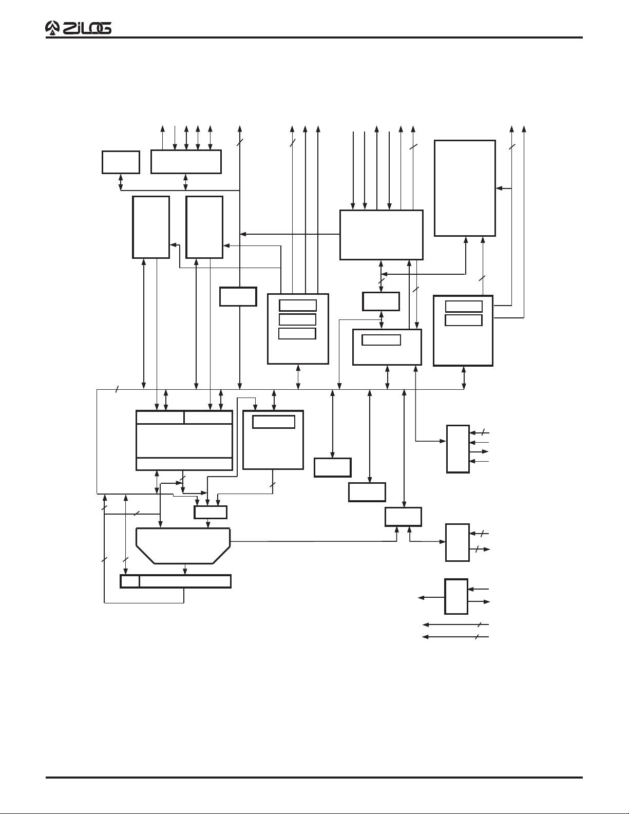
GENERAL DESCRIPTION (Continued)
Z89462
CP95DSP0400
IDB
Timers
RAM0
512W
TxD
SCLK
RxD
CODEC
FS0
RAM1
512W
FS1
MD15-MD0
16
MDR
MA15-MA0
MRD//WR
16
MAR
SP
FPR
MBUS_RAM01
Control
/MDS
AIT
AIT
/PDS
/PW
/MW
WSG_BYWD
16
PDR
IR
DSP Control
/PALSB
/PDSZE
ds
PD15-PD0
16
2
waits
Program
RAM
1KW
rd,wr
PAR
PC
PBUS
Control
A0
PRD//WR
PA15-P
16
2
16
32
16
X
Multiplier
PH
32
BA
8
AE
AH AL
Y
PPL
32
PB BFB
MUX
ALU
A
BFR
Bit
Field
Unit
32
Repeat
Count
Reg
RC
CR
Control
Reg
SR
Status
Reg
INT
CTL
User
Port
CLK
GEN
2
8
2
8
3
INT2-0
/HLTHW
/HLTOUT
/RESET
UI1-0
UO1-0
CLKIN
CLK
VDD
VSS
Functional Block Diagram
2
Page 3
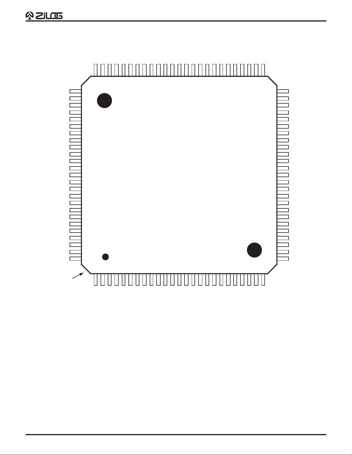
PIN DESCRIPTION
PD15
PD14
PD13
/HLTHW
PRELIMINARY
PD12
PD11
PD10
/HLTOUT
PD9
PD8
/RESET
PD7
CKIN
PD6
VSSI
PD5
CLK
/PWAIT
PD4
INT0
PD3
PDSZE
INT1
VSSP
Z89462
CP95DSP0400
VDDP
MA0
PA0
MA1
PA1
MA2
PA2
MA3
PA3
VDDP
VSSP
MA4
MA5
MA6
MA7
VSSI
MRD//WR
/MDS
/MWAIT
MA8
PA4
MA9
VDDP
VSSP
PA5
MA10
75 51
76
80
85
6070 5565
Z89462
90
95
100
100-Pin VQFP
50
26
45
40
35
30
PD2
PALSB
INT2
PD5
PRD//WR
UI1
PD1
UI0
PD0
UO1
UO0
MD15
VDDI
MD14
MD13
VSSP
VDDP
MD12
MD11
MD10
MD9
PA15
MD8
PA14
MD7
Pin 1
125
PA6
MA11
5
PA7
PA8
MA13
MA12
10 15 20
PA9
MA14
VDDP
VSSP
MA15
MD0
VDDI
MD1
MD2
MD3
PA10
MD4
VSSP
PA12
MD6
PA13
MD5
PA11
VDDP
100-Pin VQFP Pin Assignments
3
Page 4

PIN DESCRIPTION (Continued)
PRELIMINARY
Z89462
CP95DSP0400
/PAZ
PA6
MA11
PA7
MA12
PA8
MA13
PA9
MA14
VDDP
VSSP
MA15
MD0
VDDI
MD1
MD2
MD3
PA10
MD4
PA11
MD5
VDDP
VSSP
PA12
MD6
PA13
IACK
PA4
MA8
/MWAIT
/MDS
VSSI
MA10
PA5
VSSP
VDDP
FETCH
63
MA9
MRD//WR
MA7
MA6
MA5
Z89462
124-Pin PGA
MA4
VSSP
VDDP
PA3
MA3
PA2
MA2
PA1
MA1
MA0
PA0
EXEC
31
/MAZ
PD15
PD14
PD13
/HLTHW
PD12
PD11
PD10
/HLTOUT
PD9
PD8
/RESET
PD7
CKIN
PD6
VSSI
PD5
CLK
IPWAIT
PD4
INT0
PDSZE
PD3
INT1
VSSP
VDDP
93
UI1
UI0
MD7
/MDBEN
PA14
MD8
PA15
MD9
MD10
UO0
MD11
MD12
VDDP
VSSP
MD13
MD14
VDDI
MD15
UO1
PD0
PD1
/PDS
PRD//WR
INT2
PALSB
PD2
1
/BRK
124-Pin PGA Pin Assignments
4
Page 5

ABSOLUTE MAXIMUM RATINGS
PRELIMINARY
Z89462
CP95DSP0400
Description Min. Max. Units
Voltages on VDDwith Respect to V
–0.5 +5.5 V
SS
Voltages on All Pins with Respect to VSS–0.5 (VDD+0.5) V
T
STG
T
A
Storage Temp –85° +150°°C
Oper Ambient Temp 0° +70°°C
STANDARD TEST CONDITIONS
The AC and DC Characteristics listed below apply for
standard test conditions, unless otherwise noted. All
voltages are referenced to V
(= Ground = 0V). Positive
SS
current flows into the referenced pin. Standard conditions
are as follows:
DC ELECTRICAL CHARACTERISTICS
(5.0V Operation)
Stresses greater than those listed under Absolute Maximum
Ratings may cause permanent damage to the device. This
is a stress rating only; operation of the device at any
condition above those indicated in the operational sections
of these specifications is not implied. Exposure to absolute
maximum rating conditions for extended period may affect
device reliability.
3.0V < VDD < 3.6V
VSS = 0V
Ambient Temperature = 0°C to +70°C
Standard Test Load on All Outputs
Sym. Parameter Min. Max. Unit Note
V
IH
V
IL
V
OH1
V
OH2
V
OL
I
IL
I
TL
I
DD
I
DD2
C
IN
C
OUT
C
IO
C
L
Notes:
[1] VIN = 0.4V
[2] 0.4V < V
[3] VDD = 5.0V, VIH = 4.8V, VIL = 0.2V
[4] VDD = 5.0V, VIH = 4.8V, VIL = 0.2V
[5] Unmeasured pins returned to VSS.
Input High Voltage 2.0 VDD +0.5 V
Input Low Voltage –0.5 0.8 V
Output High Voltage (–4 mA IOH) 2.4 V
Output High Voltage (–250 µA I
)V
OH
–0.8 V
DD
Output Low Voltage (4 mA IOL) 0.5 V
Input Leakage Current –10 +10 µA [1]
Tri-State Leakage Current –10 +10 µA [2]
Power Supply Current (@ 40 Mhz) TBD mA [3]
Stopped Clock Power Supply Current 20 µA [4]
Input Capacitance (f = 1 MHz) 15 pF [5]
Output Capacitance (f = 1 Mhz) 15 pF [5]
I/O Capacitance (f = 1 MHz) 15 pF [5]
Output Load Capacitance 30 pF
< 2.4V
OUT
5
Page 6

PRELIMINARY
AC ELECTRICAL CHARACTERISTICS
(5.0V Operation)
Symbol Parameter Min. Max. Unit Note
TcCI CLKIN Cycle Time 25 ns
TwCIh CLKIN Width High 10 ns
TwCIl CLKIN Width Low 10 ns
TrCI CLKIN Rise Time 2 ns
TfCI CLKIN Fall Time 2 ns
TdCIr(Cr) CLKIN Rise to CLK Rise Delay 8 ns
TdCIf(Cf) CLKIN Fall to CLK Fall Delay 8 ns
TrC CLK Rise Time 2 ns
TfC CLK Fall Time 2 ns
TdCr(PA) CLK Rise to PA Valid Delay 5 ns
TdCr(PALSB) CLK Rise to PALSB Valid Delay 5 ns
TdCr(PDSr) CLK Rise to /PDS Rise Delay 4 ns
TdCf(PDSf) CLK Fall to /PDS Fall Delay 4 ns
TsPW(Cr) /PWAIT to CLK Rise Setup Time 5 ns
ThPW(Cr) /PWAIT to CLK Rise Hold Time 0 ns
Z89462
CP95DSP0400
TsPSZ(Cr) PDSZE to CLK Rise Setup Time 5 ns
ThPSZ(Cr) PDSZE to CLK Rise Hold Time 0 ns
TdCr(PRDWR) CLK Rise to PRD//WR Delay 5 ns
TsPD(Cr) PD to CLK Rise Setup Time 5 ns
ThPD(Cr) PD to CLK Rise Hold Time 0 ns
TdCR(PD) CLK Rise to PD Valid Delay 5 ns
TdCr(PDt) CLK Rise to PD Tri-State Delay 5 ns
TdCr(MA) CLK Rise to MA Valid Delay 5 ns
TdCr(MDSr) CLK Rise to /MDS Rise Delay 4 ns
TdCf(MDSf) CLK Rise to /MDS Fall Delay 4 ns
TsMW(Cr) /MWAIT to CLK Rise Setup Time 5 ns
ThMW(Cr) /MWAIT to CLK Rise Hold Time 0 ns
TdCr(MRDWR) CLK Rise to MRD//WR Delay 5 ns
TsMD(Cr) MD to CLK Rise Setup Time 5 ns
ThMD(Cr) MD to CLK Rise Hold Time 0 ns
TdCr(MD) CLK Rise to MD Valid Delay 5 ns
TdCr(MDt) CLK Rise to MD Tri-State Delay 5 ns
TsINT(Cr) INT2-0 to CLK Rise Setup Time 5 ns [1]
TwINTh INT2-0 Width High 10 ns
TwHLTHWl /HLTHW Width Low 10 TcCI [2]
TwHLTHWh /HLTHW Width High 2 TcCI [2]
TdCr(HLTOUT) CLK Rise to HLTOUT Delay 5 ns
TwRESETl /RESET Width Low 3 TcCI [2]
Notes:
[1] INT2-0 can also be asserted/deasserted asynchronously.
[2] These signals are asserted/deasserted asynchronously.
.
6
Page 7

PRELIMINARY
DC ELECTRICAL CHARACTERISTICS
(3.0V Operation)
Sym. Parameter Min. Max. Unit Note
Z89462
CP95DSP0400
V
IH
V
IL
V
OH
V
OL
I
IL
I
TL
I
DD
I
DD2
C
IN
C
OUT
C
IO
C
L
Notes:
[1] VIN = 0.4V
[2] 0.4V < V
[3] VDD = 3.3V, VIH = 3.0V, VIL = 0.2V
[4] VDD = 3.3V, VIH = 3.0V, VIL = 0.2V
[5] Unmeasured pins returned to VSS.
Input High Voltage 2.0 VDD +0.5 V
Input Low Voltage –0.5 0.6 V
Output High Voltage (–200 µA I
Output Low Voltage (4 mA IOL) 0.4 V
Input Leakage Current –10 +10 µA [1]
Tri-State Leakage Current –10 +10 µA [2]
Power Supply Current (@ 40 Mhz) TBD mA [3]
Stopped Clock Power Supply Current 20 µA [4]
Input Capacitance (f = 1 MHz) 15 pF [5]
Output Capacitance (f = 1 Mhz) 15 pF [5]
I/O Capacitance (f = 1 MHz) 15 pF [5]
Output Load Capacitance 30 pF
< 2.15V
OUT
) 2.15 V
OH
7
Page 8

PRELIMINARY
Z89462
CP95DSP0400
Pre-Characterization Product:
The product represented by this CPS is newly introduced
and Zilog has not completed the full characterization of the
product. The CPS states what Zilog knows about this
product at this time, but additional features or non-
Development Projects:
Customer is cautioned that while reasonable efforts will be
employed to meet performance objectives and milestone
dates, development is subject to unanticipated problems
Low Margin:
Customer is advised that this product does not meet
Zilog’s internal guardbanded test policies for the
specification requested and is supplied on an exception
basis. Customer is cautioned that delivery may be uncertain
© 1995 by Zilog, Inc. All rights reserved. No part of this document
may be copied or reproduced in any form or by any means
without the prior written consent of Zilog, Inc. The information in
this document is subject to change without notice. Devices sold
by Zilog, Inc. are covered by warranty and patent indemnification
provisions appearing in Zilog, Inc. Terms and Conditions of Sale
only. Zilog, Inc. makes no warranty, express, statutory, implied or
by description, regarding the information set forth herein or
regarding the freedom of the described devices from intellectual
property infringement. Zilog, Inc. makes no warranty of merchantability or fitness for any purpose. Zilog, Inc. shall not be
responsible for any errors that may appear in this document.
Zilog, Inc. makes no commitment to update or keep current the
information contained in this document.
conformance with some aspects of the CPS may be found,
either by Zilog or its customers in the course of further
application and characterization work. In addition, Zilog
cautions that delivery may be uncertain at times, due to
start-up yield issues.
and delays. No production release is authorized or
committed until the Customer and Zilog have agreed upon
a Customer Procurement Specification for this project.
and that, in addition to all other limitations on Zilog liability
stated on the front and back of the acknowledgement,
Zilog makes no claim as to quality and reliability under the
CPS. The product remains subject to standard warranty for
replacement due to defects in materials and workmanship.
Zilog’s products are not authorized for use as critical components in life support devices or systems unless a specific written
agreement pertaining to such intended use is executed between
the customer and Zilog prior to use. Life support devices or
systems are those which are intended for surgical implantation
into the body, or which sustains life whose failure to perform,
when properly used in accordance with instructions for use
provided in the labeling, can be reasonably expected to result in
significant injury to the user.
Zilog, Inc. 210 East Hacienda Ave.
Campbell, CA 95008-6600
Telephone (408) 370-8000
Telex 910-338-7621
FAX 408 370-8056
Internet: http://www.zilog.com
8
 Loading...