

Page 1
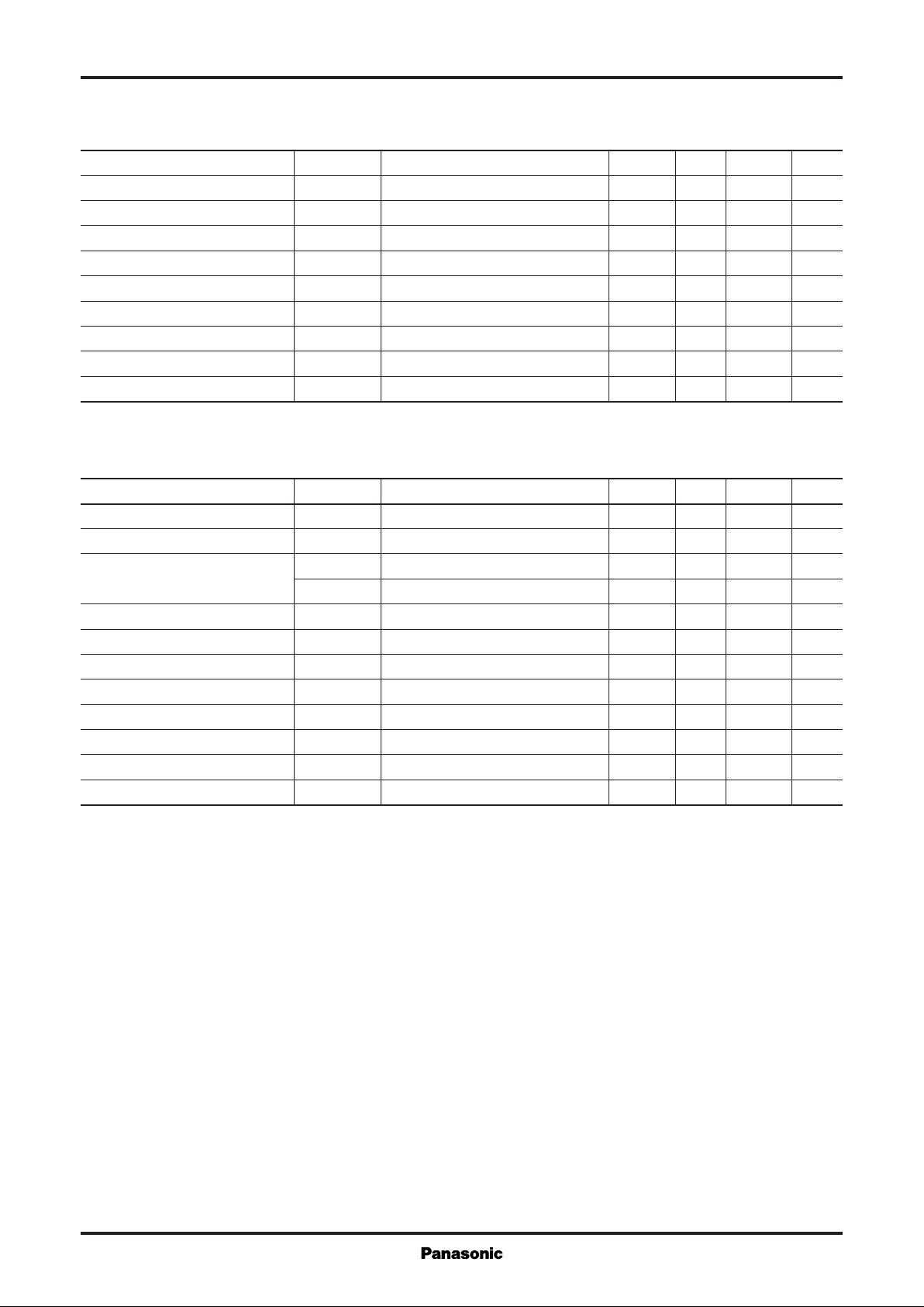
Composite Transistors
XP8081
Silicon N-channel junction FET (Tr1)
Silicon NPN epitaxial planer transistor (Tr2)
For analog switching (Tr1)/switching (Tr2)
Features
■
●
Two elements incorporated into one package.
●
Reduction of the mounting area and assembly cost by one half.
Basic Part Number of Element
■
●
2SK1103+UN1213 (transistors with built-in resistor)
Absolute Maximum Ratings (Ta=25˚C)
■
Parameter Symbol Ratings Unit
Tr1
Tr2
Overall
Gate to drain voltage
Drain current I
Gate current I
Collector to base voltage
Collector to emitter voltage
Collector current I
Total power dissipation
Junction temperature
Storage temperature
V
GDS
D
G
V
CBO
V
CEO
C
P
T
T
j
T
stg
–50 V
20 mA
10 mA
50 V
50 V
100 mA
150 mW
150 ˚C
–55 to +150 ˚C
2.1±0.1
1.25±0.1
0.425 0.425
1
0.650.65
2
2.0±0.10.9±0.1
3
0.2
0.7±0.1
0 to 0.1
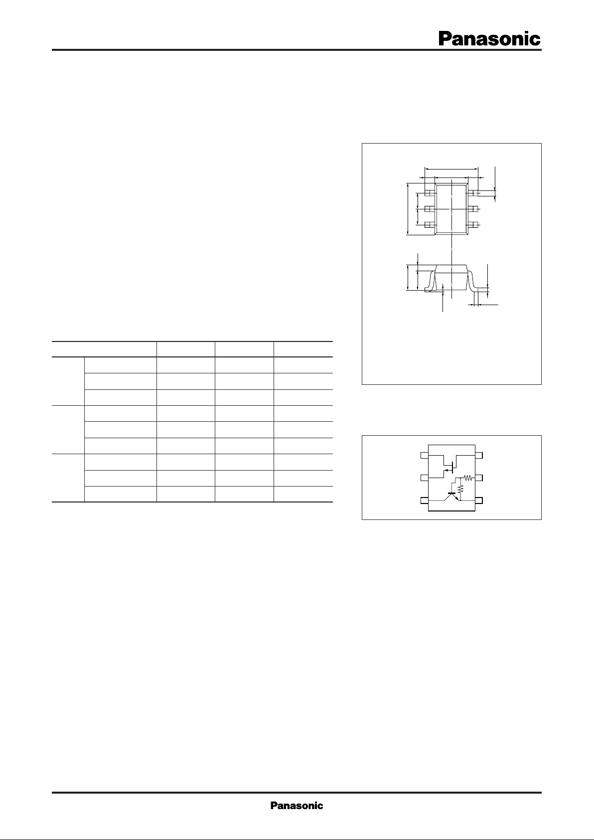
1 : Drain (Tr1) 4 : Emitter (Tr2)
2 : Source (Tr1) 5 : Base (Tr2)
3 : Collector (Tr2) 6 : Gate (Tr1)
EIAJ : SC–88
S–Mini Type Package (6–pin)
Marking Symbol: 9Z
Internal Connection
1
2
34
Tr1
Tr2
6
5
4
+0.05
–0.02
0.12
0.2±0.1
6
5
Unit: mm
0.2±0.05
1
Page 2
Composite Transistors XP8081
Electrical Characteristics (Ta=25˚C)
■
●
Tr1
Parameter Symbol Conditions min typ max Unit
Gate to drain voltage V
Drain current I
Gate cutoff current I
Gate to source cutoff voltage V
GDS
DSS
GSS
GSC
Mutual conductance gm VDS = 10V, ID = 1mA, f = 1kHz 1.8 2.5 mS
Drain resistance R
Common source short-circuit input capacitance
Common source reverse transfer capacitance
Common source short-circuit output capacitance
●
Tr2
C
C
C
DS(on)
iss
rss
oss
Parameter Symbol Conditions min typ max Unit
Collector to base voltage V
Collector to emitter voltage V
Collector cutoff current
Emitter cutoff current I
Forward current transfer ratio h
Collector to emitter saturation voltage
Output voltage high level V
Output voltage low level V
Transition frequency f
Input resistance R
Resistance ratio R1/R
I
I
V
CBO
CEO
EBO
FE
T
CBO
CEO
CE(sat)
OH
OL
1
2
IG = –10µA, VDS = 0 –50 V
VDS = 10V, VGS = 0 0.2 2.2 mA
VGS = –30V, VDS = 0 –10 nA
VDS = 10V, ID = 10µA –1.0 V
VDS = 10mV, VGS = 0 400 Ω
VDS = 10V, VGS = 0, f = 1MHz 7 pF
VDS = 10V, VGS = 0, f = 1MHz 1.5 pF
VDS = 10V, VGS = 0, f = 1MHz 1.5 pF
IC = 10µA, IE = 0 50 V
IC = 2mA, IB = 0 50 V
VCB = 50V, IE = 0 0.1 µA
VCE = 50V, IB = 0 0.5 µA
VEB = 6V, IC = 0 0.1 mA
VCE = 10V, IC = 5mA 80
IC = 10mA, IB = 0.3mA 0.25 V
VCC = 5V, VB = 0.5V, RL = 1kΩ 4.9 V
VCC = 5V, VB = 3.5V, RL = 1kΩ 0.2 V
VCB = 10V, IE = –1mA, f = 200MHz 150 MHz
–30% 47 +30% kΩ
0.8 1.0 1.2
2
Page 3

Composite Transistors
Common characteristics chart
XP8081
— Ta ID — V
P
T
250
)
200
mW
(
T
150
100
50
Total power dissipation P
0
02040 8060 140120100 160
Ambient temperature Ta (˚C
)
mS
(
|
fs
| Yfs | — V
5
4
3
GS
VDS=10V
Ta=25˚C
DS
2.5
2.0
)
mA
(
1.5
D
1.0
Drain current I
0.5
0
0615243
)
Drain to source voltage VDS (V
| Yfs | — I
2.5
)
mS
(
|
2.0
fs
1.5
I
DSS
=10mA
D
Ta=25˚C
VGS=0V
–0.1V
–0.2V
–0.3V
–0.4V
VDS=10V
Ta=25˚C
)
2.5
2.0
)
mA
(
1.5
D
1.0
Drain current I
0.5
0
–1.2 0–1.0 –0.2–0.8 –0.4–0.6
10
(pF)
oss
, C
rss
8
, C
iss
C
6
ID — V
GS
Ta=–25˚C
25˚C
75˚C
Gate to source voltage VGS (V
C
, C
, C
iss
— V
rss
oss
DS
VGS=0
f=1MHz
Ta=25˚C
C
iss
)
=10mA
I
DSS
2
1
Forward transfer admittance |Y
0
–1.6 –1.2 –0.8 –0.4 0
Gate to source voltage VGS (V
Characteristics charts of Tr2
— V
I
C
CE
160
140
)
120
mA
(
C
100
80
60
40
Collector current I
20
0
012210486
Collector to emitter voltage VCE (V
IB=1.0mA
0.9mA
0.8mA
Ta=25˚C
0.7mA
0.6mA
0.5mA
0.4mA
0.3mA
0.2mA
0.1mA
1.0
0.5
4
2
C
oss
C
rss
Forward transfer admittance |Y
0
Common source short-circuit input capacitance,
Common source reverse transfer capacitance,
0
02468
)
100
)
V
(
CE(sat)
0.03
Drain current ID (mA
V
30
10
3
1
0.3
0.1
–25˚C
CE(sat)
25˚C
— I
)
C
IC/IB=10
Ta=75˚C
Common source short-circuit output capacitance
1
Drain to source voltage VDS (V
400
350
FE
300
250
200
150
100
Forward current transfer ratio h
50
10 100
hFE — I
C
)
VCE=10V
Ta=75˚C
25˚C
–25˚C
Collector to emitter saturation voltage V
0.01
0.1 0.3
)
1 3 10 30 100
Collector current IC (mA
)
0
13
10 30 100 300 1000
Collector current IC (mA
)
3
Page 4

Composite Transistors XP8081
)
pF
(
ob
Cob — V
6
5
4
3
2
1
CB
f=1MHz
I
Ta=25˚C
Collector output capacitance C
0
0.1 0.3
1 3 10 30 100
Collector to base voltage VCB (V
IO — V
10000
=0
E
)
3000
)
1000
µA
(
O
300
100
30
10
Output current I
3
1
0.4
Input voltage VIN (V
IN
VO=5V
Ta=25˚C
1.41.21.00.80.6
100
30
)
10
V
(
IN
3
1
0.3
Input voltage V
0.1
0.03
0.01
0.1 0.3
)
VIN — I
1 3 10 30 100
O
VO=0.2V
Ta=25˚C
Output current IO (mA
)
4
 Loading...