

Page 1
1/26
XCL205/XCL206/XCL207
Series
Inductor Built-in Step-Down “micro DC/DC” Converters
0
20
40
60
80
100
0.1 1 10 100 1000
Output Current:I
OUT
(mA)
Efficency:EFFI(%
)
VIN= 5.5V
5.0V
4.2V
VOUT=3.3V
(
PWM
)
XCL206/XCL207(PWM/PFM
)
XCL205/XCL207
!TYPICAL PERFORMANCE
CHARACTERISTICS
"GreenOperation Compatible
!APPLICATIONS
#Mobile phones, Smart phones
#Bluetooth Headsets
#WiMAX PDAs, MIDs, UMPCs
#Portable game consoles
#Digital cameras, Camcorders
#Electronic dictionaries
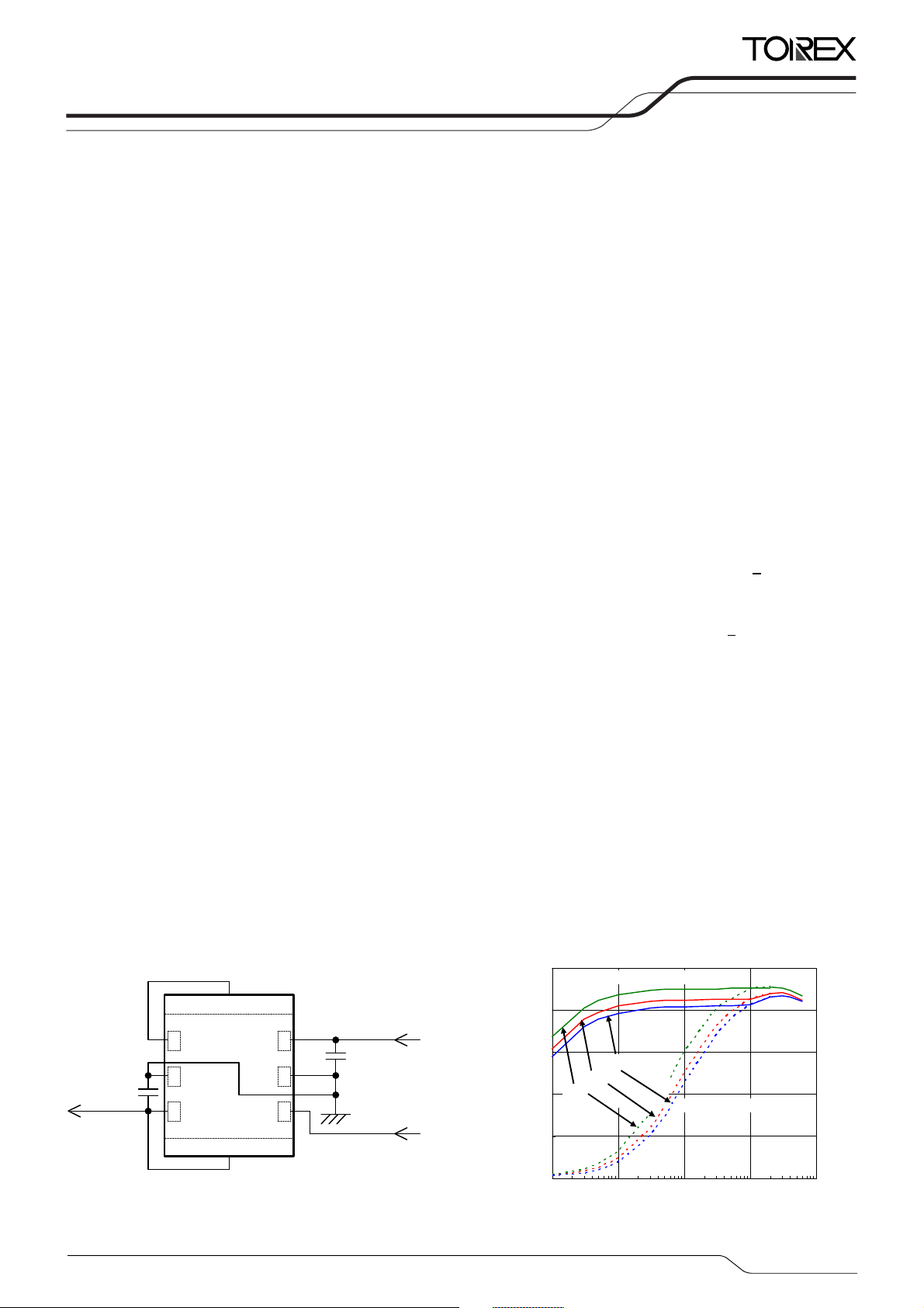
!TYPICAL APPLICATION CIRCUIT
ETR2801-006
!GENERAL DESCRIPTION
The XCL205/XCL206/XCL207 series is a synchronous step-down micro DC/DC converter which integrates an inductor and a
control IC in one tiny package (2.5mm$2.0mm, H=1.0mm). A stable power supply with an output current of 600mA is
configured using only two capacitors connected externally.
Operating voltage range is from 2.0V to 6.0V. Output voltage is internally set in a range from 0.8V to 4.0V in increments of
0.05V. The device is operated by 3.0MHz, and includes 0.42%P-channel driver transistor and 0.52%N-channel switching
transistor. As for operation mode, the XCL205 series is PWM control, the XCL206 series is automatic PWM/PFM switching
control and the XCL207 series can be manually switched between the PWM control mode and the automatic PWM/PFM
switching control mode, allowing fast response, low ripple and high efficiency over the full range of loads (from light load to
heavy load). During stand-by, the device is shutdown to reduce current consumption to as low as 1.0&A or less. With the
built-in UVLO (Under Voltage Lock Out) function, the internal driver transistor is forced OFF when input voltage becomes 1.4V
or lower. XCL205B/XCL206B/XCL207B series provide short-time turn-on by the soft start function internally set in 0.25 ms
(TYP). XCL205B(C) /XCL206 B(C) / XCL207B(C) integrate C
L
auto discharge function which enables the electric charge
stored at the output capacitor C
L
to be discharged via the internal auto-discharge switch located between the LX and VSS pins.
When the devices enter stand-by mode, output voltage quickly returns to the V
SS
level as a result of this function.
V
IN
Vss
CE/MODE
L
X
V
ss
V
OUT
CL
10&F
4.7&F
CIN
L1
L2
600mA
(TOP VIEW)
* “L1 and L
X
”, and “L2 and V
OUT
” is connected by wiring.
!FEATURES
Ultra Small : 2.5mm$2.0mm, H=1.0mm
Input Voltage : 2.0V ~ 6.0V
Output Voltage : 0.8V ~ 4.0V (+2.0%)
High Efficiency (V
OUT
=1.8V) : 85% (TYP.)
Output Current : 600mA
Oscillation Frequency : 3.0MHz (+15%)
Maximum Duty Cycle
Capacitor
CE Function
Protection Circuits
: 100%
: Low ESR Ceramic
: Active High
Soft-Start Circuit Built-In
C
L
High Speed Auto Discharge
:Current Limiter Circuit Built-In
(Constant Current & Latching)
Control Methods : PWM (XCL205)
PWM/PFM Auto (XCL206)
PWM/PFM Manual (XCL207)
* Performance depends on external components and wiring on the PCB.
XCL205A333xx/XCL206A333xx/XCL207A333xx
XCL205/206/207 Series
Page 2

PIN NUMBER PIN NAME
FUNCTION
1 Lx Switching Output
2,5 VSS Ground
3 V
OUT
Output Voltage
4 CE / MODE Chip Enable & Mode Switch
6 VIN Power Input
7 L1
8 L2
Inductor Electrodes
DESIGNATOR DESCRIPTION SYMBOL DESCRIPTION
A
No CL auto discharge, Standard soft-start
B
CL auto discharge, High speed soft-start
'
Functions selection
(All CE active high)
C
C
L
auto discharge, Standard soft-start
10 1.0V
12 1.2V
14 1.4V
15 1.5V
18 1.8V
19 1.9V
25 2.5V
28 2.8V
2L 2.85V
30 3.0V
()
Output Voltage
(*2)
33 3.3V
* Oscillation Frequency
3 3.0MHz
+,--
Packages
Taping Type
(*3)
AR-G XCL205/6/7
!"##"$ %&'()
*+
*,
-
.
%
&/
0
%
11
2
3'4$"5'
6
+
*7
, % 11
8 %
"9#
* It should be connected the V
SS pin (No. 2 and 5) to the GND pin.
* If the dissipation pad needs to be connected to other pins, it should be
connected to the GND pin.
* Please refer to pattern layout page for the connecting to PCB.
(*1)
The “-G” suffix indicates that the products are Halogen and Antimony free as well as being fully RoHS compliant.
(*2)
When other output voltages are needed, please contact your local Torex sales office for more information.
Output voltage range is 0.8~4.0V.
(*3)
The device orientation is fixed in its embossed tape pocket.
XCL205/XCL206/XCL207
Series
!PIN CONFIGURATION
!PIN ASSIGNMENT
!PRODUCT CLASSIFICATION
#Ordering Information
XCL205'()*+,-XCL206'()*+,-XCL207'()*+,--
(*1)
Fixed PWM control
(*1)
PWM / PFM automatic switching control
(*1)
Manual Mode Selection Pin (Semi-custom)
2/26
Page 3
PARAMETER SYMBOL RATINGS UNITS
VIN Pin Voltage VIN - 0.3 ~ 6.5 V
LX Pin Voltage VLX - 0.3 ~ VIN + 0.3/6.5 V
V
OUT
Pin Voltage V
OUT
- 0.3 ~ 6.5 V
CE/MODE Pin Voltage VCE - 0.3 ~ 6.5 V
LX Pin Current ILX 01500 mA
Power Dissipation Pd 1000*1 mW
Operating Temperature Range Topr - 40 ~ + 85 .
Storage Temperature Range Tstg - 40 ~ + 105 .
#XCL205A / XCL206A / XCL207A series
NOTE: The XCL205 offers a fixed PWM control, a signal from CE/MODE Control Logic to PWM/PFM Selector is fixed to "L" level inside.
The XCL206 control scheme is PWM/PFM automatic switching, a signal from CE/MODE Control Logic to PWM/PFM Selector is fixed to
"H" level inside. The diodes placed inside are ESD protection diodes and parasitic diodes.
3'4$"5'
:,
:+
';;<;=>?@A
%;BC=DEFG
H<CF=HFI;FJ
3'
KGI1B
3<?@BL1IFE<L
K($4KM$
HBNBOF<;
3P;;BLF=MBBQRIOS
3P;;BLF=*E?EF
K($
3<?@I;IF<;
*<TEO
HULOG
!PCCB;
5;EVB
:8
:6
9%*"
9%*"=3?@
:I?@=(IVB
WBLB;IF<;
"H3
*7
%
HH
%&/
%"9#
3'4$"5'
3<LF;<N
*<TEO
%HX":#
M!
3M!
&LQPOF<;
%HH
*, *+
*1: The power dissipation figure shown is PCB mounted (40mm$40mm, t=1.6mm, Glass Epoxy FR-4).
Please refer to page 16 for details.
#XCL205B / XCL206B / XCL207B / XCL205C / XCL206C / XCL207C series
3'4$"5'
:,
:+
';;<;=>?@A
%;BC=DEFG
H<CF=HFI;FJ
3'
KGI1B
3<?@BL1IFE<L
K($4KM$
HBNBOF<;
3P;;BLF=MBBQRIOS
3P;;BLF=*E?EF
K($
3<?@I;IF<;
*<TEO
HULOG
!PCCB;
5;EVB
:8
:6
9%*"
9%*"=3?@
:I?@=(IVB
WBLB;IF<;
"H3
*7
%HH
%&/
%"9#
3'4$"5'
3<LF;<N
*<TEO
3'4
%HX":#
M!
3M!
%HH
&LQPOF<;
*, *+
NOTE: The XCL205 offers a fixed PWM control, a signal from CE/MODE Control Logic to PWM/PFM Selector is fixed to "L" level inside.
The XCL206 control scheme is PWM/PFM automatic switching, a signal from CE/MODE Control Logic to PWM/PFM Selector is fixed to
"H" level inside. The diodes placed inside are ESD protection diodes and parasitic diodes.
XCL205/XCL206/XCL207
!BLOCK DIAGRAM
Series
!ABSOLUTE MAXIMUM RATINGS
Ta = 25.
3/26
Page 4
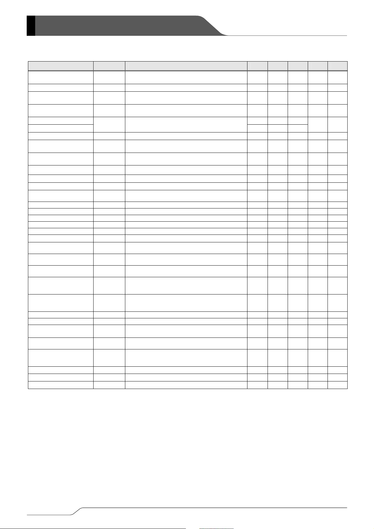
PARAMETER SYMBOL CONDITIONS MIN. TYP. MAX. UNITS
CIRCUIT
Output Voltage V
OUT
When connected to external components,
V
IN=VCE
=5.0V, I
OUT
=30mA
1.176 1.200 1.224 V '
Operating Voltage Range VIN 2.0 - 6.0 V '
Maximum Output Current I
OUTMAX
V
IN=VOUT(T)
+2.0V, VCE=1.0V
When connected to external components
(*9)
600 - - mA '
UVLO Voltage V
UVLO
V
CE=VIN,VOUT
=0V,
Voltage which Lx pin holding “L” level
(*1, *11)
1.00 1.40 1.78 V )
Supply Current (XCL205) - 46 65
Supply Current (XCL206, XCL207)
IDD VIN=VCE=5.0V, V
OUT=VOUT(T)
$1.1V
- 21 35
&A (
Stand-by Current I
STB
VIN=5.0V, VCE=0V, V
OUT=VOUT(T)
$1.1V - 0 1.0 &A (
Oscillation Frequency f
OSC
When connected to external components,
V
IN=VOUT(T)
+2.0V,VCE=1.0V, I
OUT
=100mA
2550 3000 3450 kHz '
PFM Switching Current
(*12)
I
PFM
When connected to external components,
V
IN=VOUT(T)
+2.0V, VCE=VIN , I
OUT
=1mA
(*12)
190 260 350 mA 1
PFM Duty Limit
(*12)
DTY
LIMIT_PFM
V
CE
= VIN=(C-1) I
OUT
=1mA
(*12)
- 200 300 % '
Maximum Duty Cycle
D
MAX
V
IN=VCE
=5.0V, V
OUT=VOUT (T)
$0.9V 100 - - % )
Minimum Duty Cycle
D
MIN
V
IN=VCE
=5.0V, V
OUT=VOUT (T)
$1.1V - - 0 % )
Efficiency
EFFI
When connected to external components,
V
CE=VIN2VOUT (T)
+1.2V, I
OUT
= 100mA
- 82 - % '
Lx SW "H" ON Resistance 1 R
L3H
VIN=VCE=5.0V, V
OUT
=0V, ILX=100mA
(*3)
- 0.35 0.55 % *
Lx SW "H" ON Resistance 2 R
L3H
VIN=VCE=3.6V, V
OUT
=0V, ILX=100mA
(*3)
- 0.42 0.67 % *
Lx SW "L" ON Resistance 1 R
L3L
VIN=VCE=5.0V
(*4)
- 0.45 0.66 % -
Lx SW "L" ON Resistance 2 R
L3L
VIN=VCE=3.6V,
(*4)
- 0.52 0.77 % -
Lx SW "H" Leak Current
(*5)
ILeakH VIN=V
OUT
=5.0V, VCE=0V, LX=0V - 0.01 1.0 &A +
Lx SW "L" Leak Current
(*5)
ILeakL VIN=V
OUT
=5.0V, VCE=0V, LX= 5.0V - 0.01 1.0 &A +
Current Limit
(*10)
I
LIM
VIN=VCE=5.0V, V
OUT=VOUT (E)
$0.9V
(*8)
900 1050 1350 mA ,
Output Voltage
Temperature Characteristics
4
V
OUT
/
(V
OUT
54
topr)
I
OUT
=30mA
-40./Topr/85.
- 0100 - ppm/ . '
CE "H" Voltage V
CEH
V
OUT
=0V, Applied voltage to VCE,
Voltage changes Lx to “H” level
(*11)
0.65 - V
IN
V )
CE "L" Voltage V
CEL
V
OUT
=0V, Applied voltage to VCE,
Voltage changes Lx to “L” level
(*11)
V
SS
- 0.25 V )
PWM "H" Level Voltage
(*13)
V
PWMH
When connected to external components,
I
OUT
=1mA
(*6),
Voltage which oscillation
frequency becomes 2550kHz/f
OSC
/3450kHz
(*13)
- - VIN - 1.0 V '
PWM "L" Level Voltage
(*13)
V
PWML
When connected to external components,
I
OUT
=1mA
(*6)
, Voltage which oscillation
frequency becomes f
OSC
62550kHz
(*13)
V
IN
-
0.25
- - V '
CE "H" Current I
CEH
VIN=VCE=5.0V, V
OUT
=0V - 0.1 - 0.1 &A +
CE "L" Current I
CEL
VIN=5.0V, VCE=0V, V
OUT
=0V - 0.1 - 0.1 &A +
Soft Start Time tSS
When connected to external components,
V
CE
=0V7VIN , I
OUT
=1mA
0.5 0.9 2.5 ms '
Latch Time t
LAT
V
IN
=
VCE=5.0V,
V
OUT
=0.8$V
OUT
(T)
Short Lx at 1% resistance
(*7)
1.0 - 20 ms -
Short Protection
Threshold Voltage
V
SHORT
Sweeping V
OUT
, VIN=VCE=5.0V, Short Lx at
1% resistance, V
OUT
voltage which Lx becomes “L”
level within 1ms
0.450 0.600 0.750 V -
Inductance Value L Test frequency=1MHz - 1.5 - &H
Allowed Inductor Current IDC 8T=40. - 1000 - mA
Test conditions: Unless otherwise stated, VIN=5.0V, VOUT (T)=Nominal Voltage
NOTE:
*1: Including hysteresis operating voltage range.
*2: EFFI = { ( output voltage$output current ) 9 ( input voltage$input current) }$100
*3: ON resistance (%)= (V
IN - Lx pin measurement voltage) 9 100mA
*4: Design value
*5: When temperature is high, a current of approximately 10&A (maximum) may leak.
*6: The CE/MODE pin of the XCL207 series works also as an external switching pin of PWM control and PWM/PFM control. When the IC is in the
operation, control is switched to the automatic PWM/PFM switching mode when the CE/MODE pin voltage is equal to or greater than V
IN minus
0.3V, and to the PWM mode when the CE/MODE pin voltage is equal to or lower than V
IN minus 1.0V and equal to or greater than VCEH.
*7: Time until it short-circuits V
OUT with GND via 1%of resistor from an operational state and is set to Lx=0V from current limit pulse generating.
*8: When V
IN is less than 2.4V, limit current may not be reached because voltage falls caused by ON resistance.
*9: When the difference between the input and the output is small, some cycles may be skipped completely before current maximizes.
If current is further pulled from this state, output voltage will decrease because of P-ch driver ON resistance.
*10: Current limit denotes the level of detection at peak of coil current.
*11: “H”=V
IN~VIN-1.2V, “L”=+0.1V~-0.1V
*12: I
PFM and DTY
LIMIT_PFM
are defined only for the XCL206 and XCL207 series which have PFM control function. (Not for the XCL 205 series)
*13: V
PWMH and VPWML are defined onl
y
for the XCL207 series. (They are not used in the XCL205/and XCL206 series)
XCL205/XCL206/XCL207
Series
!ELECTRICAL CHARACTERISTICS
#XCL205A123AR/XCL206A123AR/XCL207A123AR, V
OUT
=1.2V, f
4/26
=3.0MHz, Ta=25Y=
OSC
Page 5
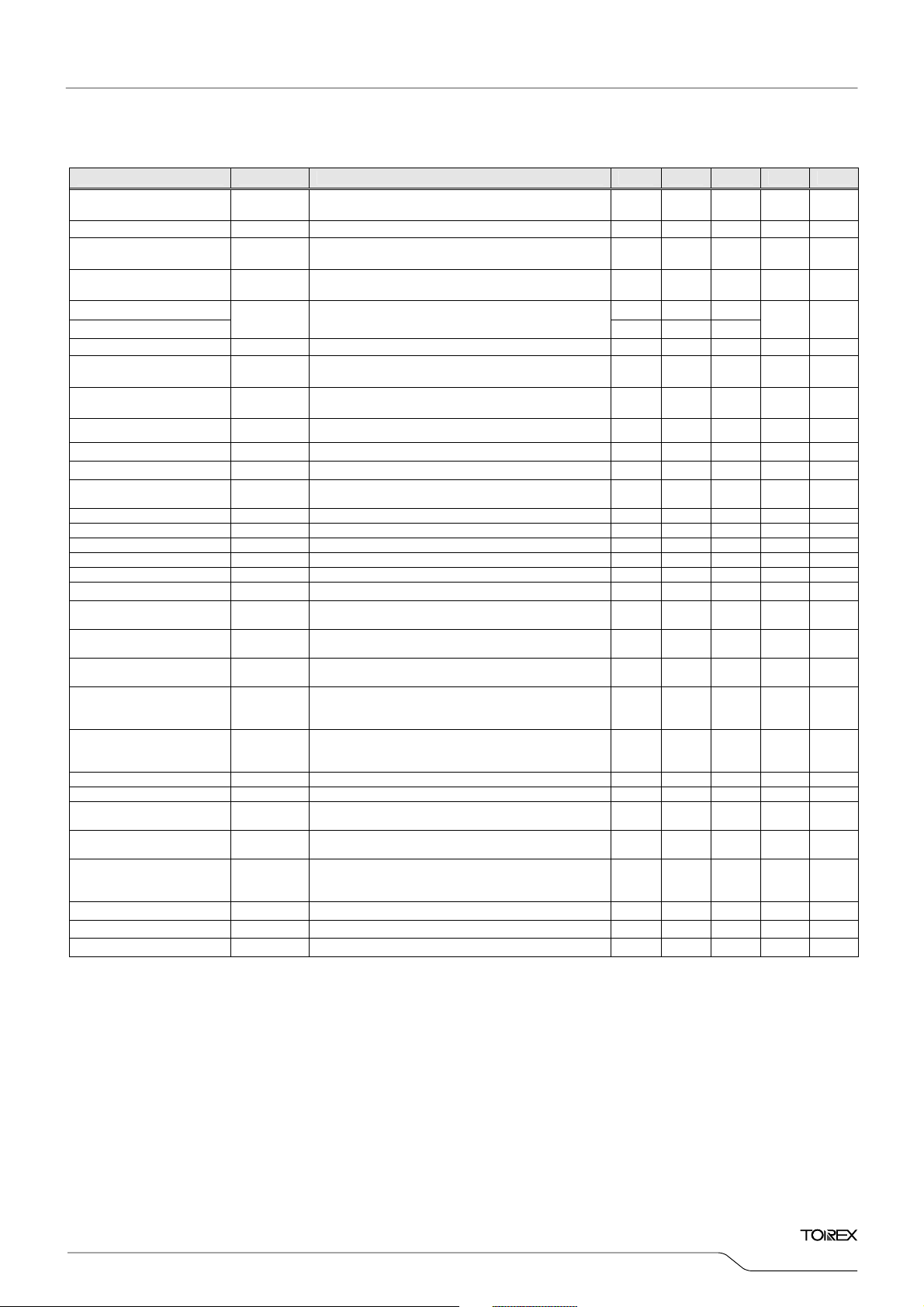
PARAMETER SYMBOL CONDITIONS MIN. TYP. MAX. UNITS
CIRCUIT
Output Voltage V
OUT
When connected to external components,
V
IN=VCE
=5.0V, I
OUT
=30mA
1.764 1.800 1.836 V '
Operating Voltage Range VIN 2.0 - 6.0 V '
Maximum Output Current I
OUTMAX
V
IN=VOUT(E)
+2.0V, VCE=1.0V
When connected to external components
(*9)
600 - - mA '
UVLO Voltage V
UVLO
V
CE=VIN,VOUT
=0V,
Voltage which Lx pin holding “L” level
(*1, *11)
1.00 1.40 1.78 V )
Supply Current (XCL205) - 46 65
Supply Current (XCL206, XCL207)
I
DD
VIN=VCE=5.0V, V
OUT=VOUT(T)
$1.1V
- 21 35
&A (
Stand-by Current I
STB
VIN=5.0V, VCE=0V, V
OUT=VOUT(T)
$1.1V - 0 1.0 &A (
Oscillation Frequency f
OSC
When connected to external components,
V
IN=VOUT(T)
+2.0V,VCE=1.0V, I
OUT
=100mA
2550 3000 3450 kHz '
PFM Switching Current
(*12)
I
PFM
When connected to external components,
V
IN=VOUT(T)
+2.0V, VCE=VIN , I
OUT
=1mA
(*12)
170 220 270 mA 1
PFM Duty Limit
(*12)
DTY
LIMIT_PFM
V
CE
= VIN=(C-1) I
OUT
=1mA
(*12)
- 200 300 % '
Maximum Duty Cycle D
MAX
VIN=VCE=5.0V, V
OUT=VOUT (T)
$0.9V 100 - - % )
Minimum Duty Cycle D
MIN
VIN=VCE=5.0V, V
OUT=VOUT (T)
$1.1V - - 0 % )
Efficiency EFFI
When connected to external components,
V
CE=VIN2VOUT (T)
+1.2V, I
OUT
= 100mA
- 85 - % '
Lx SW "H" ON Resistance 1 R
L3H
VIN=VCE=5.0V, V
OUT
=0V, ILX=100mA
(*3)
- 0.35 0.55 % *
Lx SW "H" ON Resistance 2 R
L3H
VIN=VCE=3.6V, V
OUT
=0V, ILX=100mA
(*3)
- 0.42 0.67 % *
Lx SW "L" ON Resistance 1 R
L3L
VIN=VCE=5.0V
(*4)
- 0.45 0.66 % -
Lx SW "L" ON Resistance 2 R
L3L
VIN=VCE=3.6V,
(*4)
- 0.52 0.77 % -
Lx SW "H" Leak Current
(*5)
ILeakH VIN=V
OUT
=5.0V, VCE=0V, LX=0V - 0.01 1.0 &A +
Lx SW "L" Leak Current
(*5)
ILeakL VIN=V
OUT
=5.0V, VCE=0V, LX= 5.0V - 0.01 1.0 &A +
Current Limit
(*10)
I
LIM
VIN=VCE=5.0V, V
OUT=VOUT (E)
$0.9V
(*8)
900 1050 1350 mA ,
Output Voltage
Temperature Characteristics
4
V
OUT
/
(V
OUT
54
topr)
I
OUT
=30mA
-40./Topr/85.
- 0100 - ppm/ . '
CE "H" Voltage V
CEH
V
OUT
=0V, Applied voltage to VCE,
Voltage changes Lx to “H” level
(*11)
0.65 - V
IN
V )
CE "L" Voltage V
CEL
V
OUT
=0V, Applied voltage to VCE,
Voltage changes Lx to “L” level
(*11)
V
SS
- 0.25 V )
PWM "H" Level Voltage
(*13)
V
PWMH
When connected to external components,
I
OUT
=1mA
(*6),
Voltage which oscillation
frequency becomes 2550kHz/f
OSC
/3450kHz
(*13)
- - VIN - 1.0 V '
PWM "L" Level Voltage
(*13)
V
PWML
When connected to external components,
I
OUT
=1mA
(*6)
, Voltage which oscillation
frequency becomes f
OSC
62550kHz
(*13)
V
IN
-
0.25
- - V '
CE "H" Current I
CEH
VIN=VCE=5.0V, V
OUT
=0V - 0.1 - 0.1 &A +
CE "L" Current I
CEL
VIN=5.0V, VCE=0V, V
OUT
=0V - 0.1 - 0.1 &A +
Soft Start Time tSS
When connected to external components,
V
CE
=0V7VIN , I
OUT
=1mA
0.5 0.9 2.5 ms '
Latch Time t
LAT
V
IN
=
VCE=5.0V,
V
OUT
=0.8$V
OUT
(T)
Short Lx at 1% resistance
(*7)
1.0 - 20 ms -
Short Protection
Threshold Voltage
V
SHORT
Sweeping V
OUT
, VIN=VCE=5.0V, Short Lx at
1% resistance, V
OUT
voltage which Lx becomes “L”
level within 1ms
0.675 0.900 1.125 V -
Inductance Value L Test frequency =1MHz - 1.5 - &H
Allowed Inductor Current IDC 8T=40. - 1000 - mA
Test conditions: Unless otherwise stated, VIN=5.0V, VOUT (T)=Nominal Voltage
NOTE:
*1: Including hysteresis operating voltage range.
*2: EFFI = { ( output voltage$output current ) 9 ( input voltage$input current) }$100
*3: ON resistance (%)= (V
IN - Lx pin measurement voltage) 9 100mA
*4: Design value
*5: When temperature is high, a current of approximately 10&A (maximum) may leak.
*6: The CE/MODE pin of the XCL207 series works also as an external switching pin of PWM control and PWM/PFM control. When the IC is in the
operation, control is switched to the automatic PWM/PFM switching mode when the CE/MODE pin voltage is equal to or greater than V
IN minus
0.3V, and to the PWM mode when the CE/MODE pin voltage is equal to or lower than V
IN minus 1.0V and equal to or greater than VCEH.
*7: Time until it short-circuits V
OUT with GND via 1%of resistor from an operational state and is set to Lx=0V from current limit pulse generating.
*8: When V
IN is less than 2.4V, limit current may not be reached because voltage falls caused by ON resistance.
*9: When the difference between the input and the output is small, some cycles may be skipped completely before current maximizes.
If current is further pulled from this state, output voltage will decrease because of P-ch driver ON resistance.
*10: Current limit denotes the level of detection at peak of coil current.
*11: “H”=V
IN~VIN-1.2V, “L”=+0.1V~-0.1V
*12:
IPFM and DTY
LIMIT_PFM
are defined only for the XCL206 and XCL207 series which have PFM control function. (Not for the XCL 205 series)
*13: V
PWMH and VPWML are defined only for the XCL207 series. (They are not used in the XCL205/and XCL206 series)
!ELECTRICAL CHARACTERISTICS (Continued)
#XCL205A183AR/XCL206A183AR/XCL207A183AR, V
OUT
=1.8V, f
=3.0MHz, Ta=25Y=
OSC
XCL205/XCL206/XCL207
Series
5/26
Page 6
PARAMETER SYMBOL CONDITIONS MIN. TYP. MAX. UNITS
CIRCUIT
Output Voltage
V
OUT
When connected to external components,
V
IN=VCE
=5.0V, I
OUT
=30mA
1.176 1.200 1.224 V '
Operating Voltage Range
V
IN
2.0 - 6.0 V '
Maximum Output Current
I
OUTMAX
V
IN=VOUT(T)
+2.0V, VCE=1.0V
When connected to external components
(*9)
600 - - mA '
UVLO Voltage
V
UVLO
V
CE=VIN,VOUT
=0V,
Voltage which Lx pin holding “L” level
(*1, *11)
1.00 1.40 1.78 V )
Supply Current (XCL205) - 46 65
Supply Current (XCL206, XCL207)
I
DD
VIN=VCE=5.0V, V
OUT=VOUT(T)
$1.1V
- 21 35
&A (
Stand-by Current
I
STB
V
IN
=5.0V, VCE=0V, V
OUT=VOUT(T)
$1.1V
- 0 1.0 &A (
Oscillation Frequency
f
OSC
When connected to external components,
V
IN
=V
OUT(T)
+2.0V,VCE=1.0V, I
OUT
=100mA
2550 3000 3450 kHz '
PFM Switching Current
(*12)
I
PFM
When connected to external components,
V
IN
=V
OUT(T)
+2.0V, VCE = VIN , I
OUT
=1mA
(*12)
190 260 350 mA 1
PFM Duty Limit
(*12)
DTY
LIMIT_PFM
V
CE=VIN
=(C-1) I
OUT
=1mA
(*12)
- 200 300 % '
Maximum Duty Cycle D
MAX
VIN=VCE=5.0V, V
OUT=VOUT (T)
$0.9V
100 - - % )
Minimum Duty Cycle D
MIN
V
IN=VCE
=5.0V, V
OUT=VOUT (T)
$1.1V
- - 0 % )
Efficiency
EFFI
When connected to external components,
V
CE=VIN2VOUT (T)
+1.2V, I
OUT
=100mA
- 82 - % '
Lx SW "H" ON Resistance 1
R
L3H
VIN=VCE=5.0V, V
OUT
=0V, ILX=100mA
(*3)
- 0.35 0.55 % *
Lx SW "H" ON Resistance 2
R
L3H
VIN=VCE=3.6V, V
OUT
=0V, ILX=100mA
(*3)
- 0.42 0.67 % *
Lx SW "L" ON Resistance 1
R
L3L
V
IN=VCE
=5.0V
(*4)
- 0.45 0.66 % -
Lx SW "L" ON Resistance 2
R
L3L
V
IN=VCE
= 3.6V
(*4)
- 0.52 0.77 % -
Lx SW "H" Leak Current
(*5)
ILeakH
VIN=V
OUT
=5.0V, VCE =0V, LX=0V
- 0.01 1.0 &A :
Current Limit
(*10)
I
LIM
V
IN=VCE
=5.0V, V
OUT=VOUT (T)
$0.9V
(*8)
900 1050 1350 mA ,
Output Voltage
Temperature Characteristics
4
V
OUT
/
(V
OUT
54
topr)
I
OUT
=30mA
-40./Topr/85.
- 0100 - ppm/ . '
CE "H" Voltage
V
CEH
V
OUT
=0V, Applied voltage to VCE,
Voltage changes Lx to “H” level
(*11)
0.65 - V
IN
V )
CE "L" Voltage
V
CEL
V
OUT
=0V, Applied voltage to VCE,
Voltage changes Lx to “L” level
(*11)
V
SS
- 0.25 V )
PWM "H" Level Voltage
(*13)
V
PWMH
When connected to external components,
I
OUT
=1mA
(*6),
Voltage which oscillation
frequency becomes 2550kHz/f
OSC
/3450kHz
(*13)
- - VIN - 1.0 V '
PWM "L" Level Voltage
(*13)
V
PWML
When connected to external components,
I
OUT
=1mA
(*6)
, Voltage which oscillation
frequency becomes f
OSC
62550kHz
(*13)
V
IN
-
0.25
- - V '
CE "H" Current
I
CEH
VIN=VCE=5.0V, V
OUT
=0V
- 0.1 - 0.1 &A +
CE "L" Current
I
CEL
VIN=5.0V, VCE=0V, V
OUT
=0V
- 0.1 - 0.1 &A +
Soft Start Time
t
SS
When connected to external components,
V
CE
=0V7VIN , I
OUT
=1mA
- 0.25 0.40 ms '
Latch Time
t
LAT
V
IN=VCE
=5.0V, V
OUT
=0.8$V
OUT(T)
Short Lx at 1% resistance
(*7)
1.0 - 20 ms -
Short Protection
Threshold Voltage
V
SHORT
Sweeping V
OUT
, VIN=VCE=5.0V, Short Lx at
1% resistance, V
OUT
voltage which Lx becomes “L”
level within 1ms
0.450 0.600 0.750 V -
CL Discharge
R
DCHG
V
IN
=5.0V, LX=5.0V, VCE=0V, V
OUT
=Open
200 300 450 % ;
Inductance Value
L
Test frequency =1MHz
- 1.5 - &H
Allowed Inductor Current IDC
8T=40.
- 1000 - mA
Test conditions: Unless otherwise stated, VIN=5.0V, VOUT (T) =Nominal Voltage
NOTE:
*1: Including hysteresis operating voltage range.
*2: EFFI = { ( output voltage$output current ) 9 ( input voltage$input current) }$100
*3: ON resistance (%)= (V
IN - Lx pin measurement voltage) 9 100mA
*4: Design value
*5: When temperature is high, a current of approximately 10&A (maximum) may leak.
*6: The CE/MODE pin of the XCL207 series works also as an external switching pin of PWM control and PWM/PFM control. When the IC is in the
operation, control is switched to the automatic PWM/PFM switching mode when the CE/MODE pin voltage is equal to or greater than V
IN minus
0.3V, and to the PWM mode when the CE/MODE pin voltage is equal to or lower than V
IN minus 1.0V and equal to or greater than VCEH.
*7: Time until it short-circuits V
OUT with GND via 1%of resistor from an operational state and is set to Lx=0V from current limit pulse generating.
*8: When V
IN is less than 2.4V, limit current may not be reached because voltage falls caused by ON resistance.
*9: When the difference between the input and the output is small, some cycles may be skipped completely before current maximizes.
If current is further pulled from this state, output voltage will decrease because of P-ch driver ON resistance.
*10: Current limit denotes the level of detection at peak of coil current.
*11: “H”=V
IN~VIN-1.2V, “L”=+0.1V~-0.1V
*12: I
PFM and DTY
LIMIT_PFM
are defined only for the XCL206 and XCL207 series which have PFM control function. (Not for the XCL 205 series)
*13: V
PWMH and VPWML are defined only for the XCL207 series. (They are not used in the XCL205/and XCL206 series)
XCL205/XCL206/XCL207
Series
!ELECTRICAL CHARACTERISTICS (Continued)
#XCL205B123AR/XCL206B123AR/ XCL207B123AR, V
OUT
=1.2V, f
=3.0MHz, Ta=25Y=
OSC
6/26
Page 7
PARAMETER SYMBOL CONDITIONS MIN. TYP. MAX. UNITS
CIRCUIT
Output Voltage V
OUT
When connected to external components,
V
IN=VCE
=5.0V, I
OUT
=30mA
1.764 1.800 1.836 V '
Operating Voltage Range VIN 2.0 - 6.0 V '
Maximum Output Current I
OUTMAX
V
IN=VOUT(E)
+2.0V, VCE=1.0V
When connected to external components
(*9)
600 - - mA '
UVLO Voltage V
UVLO
V
CE=VIN,VOUT
=0V,
Voltage which Lx pin holding “L” level
(*1, *11)
1.00 1.40 1.78 V )
Supply Current (XCL205) - 46 65
Supply Current (XCL206, XCL207)
I
DD
VIN=VCE=5.0V, V
OUT=VOUT(T)
$1.1V
- 21 35
&A (
Stand-by Current I
STB
VIN=5.0V, VCE=0V, V
OUT=VOUT(T)
$1.1V - 0 1.0 &A (
Oscillation Frequency f
OSC
When connected to external components,
V
IN
=V
OUT(T)
+2.0V,VCE=1.0V, I
OUT
=100mA
2550 3000 3450 kHz '
PFM Switching Current
(*12)
I
PFM
When connected to external components,
V
IN
=V
OUT(T)
+2.0V, VCE = VIN , I
OUT
=1mA
(*12)
170 220 270 mA 1
PFM Duty Limit
(*12)
DTY
LIMIT_PFM
V
CE=VIN
=(C-1) I
OUT
=1mA
(*12)
- 200 300 % '
Maximum Duty Cycle D
MAX
VIN=VCE=5.0V, V
OUT=VOUT (T)
$0.9V 100 - - % )
Minimum Duty Cycle D
MIN
VIN=VCE=5.0V, V
OUT=VOUT (T)
$1.1V - - 0 % )
Efficiency EFFI
When connected to external components,
V
CE=VIN2VOUT (T)
+1.2V, I
OUT
=100mA
- 85 - % '
Lx SW "H" ON Resistance 1 R
L3H
VIN=VCE=5.0V, V
OUT
=0V, ILX=100mA
(*3)
- 0.35 0.55 % *
Lx SW "H" ON Resistance 2 R
L3H
VIN=VCE=3.6V, V
OUT
=0V, ILX=100mA
(*3)
- 0.42 0.67 % *
Lx SW "L" ON Resistance 1 R
L3L
VIN=VCE=5.0V
(*4)
- 0.45 0.66 % -
Lx SW "L" ON Resistance 2 R
L3L
VIN=VCE = 3.6V
(*4)
- 0.52 0.77 % -
Lx SW "H" Leak Current
(*5)
ILeakH VIN=V
OUT
=5.0V, VCE =0V, LX=0V - 0.01 1.0 &A :
Current Limit
(*10)
I
LIM
VIN=VCE=5.0V, V
OUT=VOUT (T)
$0.9V
(*8)
900 1050 1350 mA ,
Output Voltage
Temperature Characteristics
4
V
OUT
/
(V
OUT
54
topr)
I
OUT
=30mA
-40./Topr/85.
- 0100 - ppm/ . '
CE "H" Voltage V
CEH
V
OUT
=0V, Applied voltage to VCE,
Voltage changes Lx to “H” level
(*11)
0.65 - V
IN
V )
CE "L" Voltage V
CEL
V
OUT
=0V, Applied voltage to VCE,
Voltage changes Lx to “L” level
(*11)
V
SS
- 0.25 V )
PWM "H" Level Voltage
(*13)
V
PWMH
When connected to external components,
I
OUT
=1mA
(*6),
Voltage which oscillation
frequency becomes 2550kHz/f
OSC
/3450kHz
(*13)
- - VIN - 1.0 V '
PWM "L" Level Voltage
(*13)
V
PWML
When connected to external components,
I
OUT
=1mA
(*6)
, Voltage which oscillation
frequency becomes f
OSC
62550kHz
(*13)
V
IN
-
0.25
- - V '
CE "H" Current I
CEH
VIN=VCE=5.0V, V
OUT
=0V - 0.1 - 0.1 &A +
CE "L" Current I
CEL
VIN=5.0V, VCE=0V, V
OUT
=0V - 0.1 - 0.1 &A +
Soft Start Time tSS
When connected to external components,
V
CE
=0V7VIN , I
OUT
=1mA
- 0.32 0.50 ms '
Latch Time t
LAT
V
IN=VCE
=5.0V, V
OUT
=0.8$V
OUT(T)
Short Lx at 1% resistance
(*7)
1.0 - 20 ms -
Short Protection
Threshold Voltage
V
SHORT
Sweeping V
OUT
, VIN=VCE=5.0V, Short Lx at
1% resistance, V
OUT
voltage which Lx becomes “L”
level within 1ms
0.675 0.900 1.125 V -
CL Discharge R
DCHG
VIN=5.0V, LX=5.0V, VCE=0V, V
OUT
=Open 200 300 450 % ;
Inductance Value L Test frequency =1MHz - 1.5 - &H
Allowed Inductor Current
I
DC
8T=40. - 1000 - mA
Test conditions: Unless otherwise stated, VIN=5.0V, VOUT (T) = Nominal Voltage
NOTE:
*1: Including hysteresis operating voltage range.
*2: EFFI = { ( output voltage$output current ) 9 ( input voltage$input current) }$100
*3: ON resistance (%)= (V
IN - Lx pin measurement voltage) 9 100mA
*4: Design value
*5: When temperature is high, a current of approximately 10&A (maximum) may leak.
*6: The CE/MODE pin of the XCL207 series works also as an external switching pin of PWM control and PWM/PFM control. When the IC is in the
operation, control is switched to the automatic PWM/PFM switching mode when the CE/MODE pin voltage is equal to or greater than V
IN minus
0.3V, and to the PWM mode when the CE/MODE pin voltage is equal to or lower than V
IN minus 1.0V and equal to or greater than VCEH.
*7: Time until it short-circuits V
OUT with GND via 1%of resistor from an operational state and is set to Lx=0V from current limit pulse generating.
*8: When V
IN is less than 2.4V, limit current may not be reached because voltage falls caused by ON resistance.
*9: When the difference between the input and the output is small, some cycles may be skipped completely before current maximizes.
If current is further pulled from this state, output voltage will decrease because of P-ch driver ON resistance.
*10: Current limit denotes the level of detection at peak of coil current.
*11: “H”=V
IN~VIN-1.2V, “L”=+0.1V~-0.1V
*12: I
PFM and DTY
LIMIT_PFM
are defined only for the XCL206 and XCL207 series which have PFM control function. (Not for the XCL 205 series)
*13: V
PWMH and VPWML are defined only for the XCL207 series. (They are not used in the XCL205/and XCL206 series)
XCL205/XCL206/XCL207
!ELECTRICAL CHARACTERISTICS (Continued)
#XCL205 B183AR/XCL206 B183AR/ XCL207B183AR, V
=1.8V, f
OUT
=3.0MHz, Ta=25Y=
OSC
Series
7/26
Page 8

PARAMETER SYMBOL CONDITIONS MIN. TYP. MAX. UNITS
CIRCUIT
Output Voltage V
OUT
When connected to external components,
V
IN
= VCE =5.0V, I
OUT
=30mA
1.176 1.200 1.224 V '
Operating Voltage Range
VIN 2.0 - 6.0 V '
Maximum Output Current
I
OUTMAX
V
IN=VOUT(E)
+2.0V, VCE=1.0V
When connected to external components
(*9)
600 - - mA '
UVLO Voltage V
UVLO
V
CE=VIN,VOUT
=0V,
Voltage which Lx pin holding “L” level
(*1, *11)
1.00 1.40 1.78 V )
Supply Current (XCL205) - 46 65
Supply Current (XCL206, XCL207)
I
DD
VIN =VCE=5.0V, V
OUT
= V
OUT(T)
$1.1V
21 35
&A (
Stand-by Current I
STB
VIN =5.0V, VCE=0V, V
OUT
= V
OUT(T)
$1.1V - 0 1.0 &A (
Oscillation Frequency
f
OSC
When connected to external components,
V
IN
=V
OUT(T)
+2.0V,VCE=1.0V, I
OUT
=100mA
2550 3000 3450 kHz '
PFM Switching Current
(*12)
I
PFM
When connected to external components,
V
IN
=V
OUT(T)
+2.0V, VCE = VIN , I
OUT
=1mA
190 260 350 mA 1
PFM Duty Limit
(*12)
DTY
LIMIT_PFM
VCE= VIN =(C-1) I
OUT
=1mA - 200 300 % '
Maximum Duty Cycle MAXDTY VIN = VCE =5.0V, V
OUT
= V
OUT (T)
$0.9V 100 - - % )
Minimum Duty Cycle MINDTY VIN = VCE =5.0V, V
OUT
= V
OUT (T)
$1.1V - - 0 % )
Efficiency EFFI
When connected to external components,
V
CE
= VIN 2 V
OUT (T)
+1.2V, I
OUT
= 100mA
- 82 - % '
Lx SW "H" ON Resistance 1
R
L3H
VIN = VCE = 5.0V, V
OUT
= 0V,ILX = 100mA
(*3)
- 0.35 0.55 % *
Lx SW "H" ON Resistance 2
R
L3H
VIN = VCE = 3.6V, V
OUT
= 0V,ILX = 100mA
(*3)
- 0.42 0.67 % *
Lx SW "L" ON Resistance 1
R
L3L
VIN = VCE = 5.0V
(*4)
- 0.45 0.66 % -
Lx SW "L" ON Resistance 2
R
L3L
VIN = VCE = 3.6V
(*4)
- 0.52 0.77 % -
Lx SW "H" Leak Current
(*5)
ILeakH VIN= V
OUT
=5.0V, VCE =0V, LX=0V - 0.01 1.0 &A :
Current Limit
(*10)
I
LIM
VIN = VCE= 5.0V, V
OUT
= V
OUT (T)
$0.9V
(*8)
900 1050 1350 mA ,
Output Voltage
Temperature Characteristics
4
V
OUT
/
(V
OUT
54
topr)
I
OUT
=30mA
-40./Topr/85.
- 0100 - ppm/ . '
CE "H" Voltage V
CEH
V
OUT
=0V, Applied voltage to VCE,
Voltage changes Lx to “H” level
(*11)
0.65 - 6.0 V )
CE "L" Voltage V
CEL
V
OUT
=0V, Applied voltage to VCE,
Voltage changes Lx to “L” level
(*11)
V
SS
- 0.25 V )
PWM "H" Level Voltage
(*13)
V
PWMH
When connected to external components,
I
OUT
=1mA
(*6),
Voltage which oscillation
frequency becomes 2550kHz/f
OSC
/3450kHz
(*13)
- - VIN - 1.0 V '
PWM "H" Level Voltage
(*13)
V
PWML
When connected to external components,
I
OUT
=1mA
(*6)
, Voltage which oscillation
frequency becomes f
OSC
62550kHz
(*13)
V
IN
-
0.25
- - V '
CE "H" Current I
CEH
VIN = VCE =5.0V, V
OUT
= 0V - 0.1 - 0.1 &A +
CE "L" Current I
CEL
VIN =5.0V, VCE = 0V, V
OUT
= 0V - 0.1 - 0.1 &A +
Soft Start Time
tSS
When connected to external components,
V
CE
=0V7VIN , I
OUT
=1mA
0.5 0.9 2.5 ms '
Latch Time
t
LAT
V
IN=VCE
=5.0V, V
OUT
=0.8$V
OUT(T)
Short Lx at 1% resistance
(*7)
1.0 - 20 ms -
Short Protection
Threshold Voltage
V
SHORT
Sweeping V
OUT
, VIN=VCE=5.0V, Short Lx at
1% resistance, V
OUT
voltage which Lx becomes “L”
level within 1ms
0.450 0.600 0.750 V -
CL Discharge
R
DCHG
VIN = 5.0V LX = 5.0V VCE = 0V V
OUT
= open 200 300 450 % ;
Inductance Value
L Test frequency=1MHz - 1.5 - &H -
Allowed Inductor Current IDC
8
T=40.
- 1000 - mA -
Test conditions: Unless otherwise stated, VIN=5.0V, VOUT (T) = Nominal Voltage
NOTE:
*1: Including hysteresis operating voltage range.
*2: EFFI = { ( output voltage$output current ) 9 ( input voltage$input current) }$100
*3: ON resistance (%)= (V
IN - Lx pin measurement voltage) 9 100mA
*4: Design value
*5: When temperature is high, a current of approximately 10&A (maximum) may leak.
*6: The CE/MODE pin of the XCL207 series works also as an external switching pin of PWM control and PWM/PFM control. When the IC is in the
operation, control is switched to the automatic PWM/PFM switching mode when the CE/MODE pin voltage is equal to or greater than V
IN minus
0.3V, and to the PWM mode when the CE/MODE pin voltage is equal to or lower than V
IN minus 1.0V and equal to or greater than VCEH.
*7: Time until it short-circuits V
OUT with GND via 1%of resistor from an operational state and is set to Lx=0V from current limit pulse generating.
*8: When V
IN is less than 2.4V, limit current may not be reached because voltage falls caused by ON resistance.
*9: When the difference between the input and the output is small, some cycles may be skipped completely before current maximizes.
If current is further pulled from this state, output voltage will decrease because of P-ch driver ON resistance.
*10: Current limit denotes the level of detection at peak of coil current.
*11: “H”=V
IN~VIN-1.2V, “L”=+0.1V~-0.1V
*12: I
PFM and DTY
LIMIT_PFM
are defined only for the XCL206 and XCL207 series which have PFM control function. (Not for the XCL 205 series)
*13: V
PWMH and VPWML are defined only for the XCL207 series. (They are not used in the XCL205/and XCL206 series)
XCL205/XCL206/XCL207
Series
!ELECTRICAL CHARACTERISTICS (Continued)
#XCL205C123AR/XCL206C123AR/ XCL207C123AR, V
OUT
=1.2V, f
=3.0MHz, Ta=25Y=
OSC
8/26
Page 9

PARAMETER SYMBOL CONDITIONS MIN. TYP. MAX. UNITS
CIRCUIT
Output Voltage V
OUT
When connected to external components,
V
IN
= VCE =5.0V, I
OUT
=30mA
1.764 1.800 1.836 V '
Operating Voltage Range
V
IN
2.0 - 6.0 V '
Maximum Output Current
I
OUTMAX
V
IN=VOUT(E)
+2.0V, VCE=1.0V
When connected to external components
(*9)
600 - - mA '
UVLO Voltage V
UVLO
V
CE=VIN,VOUT
=0V,
Voltage which Lx pin holding “L” level
(*1, *11)
1.00 1.40 1.78 V )
Supply Current (XCL205) - 46 65
Supply Current (XCL206, XCL207)
I
DD
VIN =VCE=5.0V, V
OUT
= V
OUT(T)
$1.1V
- 21 35
&A (
Stand-by Current I
STB
VIN =5.0V, VCE=0V, V
OUT
= V
OUT(T)
$1.1V - 0 1.0 &A (
Oscillation Frequency
f
OSC
When connected to external components,
V
IN
=V
OUT(T)
+2.0V,VCE=1.0V, I
OUT
=100mA
2550 3000 3450 kHz '
PFM Switching Current
(*12)
I
PFM
When connected to external components,
V
IN
=V
OUT(T)
+2.0V, VCE = VIN , I
OUT
=1mA
170 220 270 mA 1
PFM Duty Limit
(*12)
DTY
LIMIT_PFM
VCE= VIN =(C-1) I
OUT
=1mA - 200 300 % '
Maximum Duty Cycle MAXDTY VIN = VCE =5.0V, V
OUT
= V
OUT (T)
$0.9V 100 - - % )
Minimum Duty Cycle MINDTY VIN = VCE =5.0V, V
OUT
= V
OUT (T)
$1.1V - - 0 % )
Efficiency EFFI
When connected to external components,
V
CE
= VIN 2 V
OUT (T)
+1.2V, I
OUT
= 100mA
- 85 - % '
Lx SW "H" ON Resistance 1
R
L3H
VIN = VCE = 5.0V, V
OUT
= 0V,ILX = 100mA
(*3)
- 0.35 0.55 % *
Lx SW "H" ON Resistance 2
R
L3H
VIN = VCE = 3.6V, V
OUT
= 0V,ILX = 100mA
(*3)
- 0.42 0.67 % *
Lx SW "L" ON Resistance 1
R
L3L
VIN = VCE = 5.0V
(*4)
- 0.45 0.66 % -
Lx SW "L" ON Resistance 2
R
L3L
VIN = VCE = 3.6V
(*4)
- 0.52 0.77 % -
Lx SW "H" Leak Current
(*5)
ILeakH VIN= V
OUT
=5.0V, VCE =0V, LX=0V - 0.01 1.0 &A :
Current Limit
(*10)
I
LIM
VIN = VCE= 5.0V, V
OUT
= V
OUT (T)
$0.9V
(*8)
900 1050 1350 mA ,
Output Voltage
Temperature Characteristics
4
V
OUT
/
(V
OUT
54
topr)
I
OUT
=30mA
-40./Topr/85.
- 0100 - ppm/ . '
CE "H" Voltage V
CEH
V
OUT
=0V, Applied voltage to VCE,
Voltage changes Lx to “H” level
(*11)
0.65 - 6.0 V )
CE "L" Voltage V
CEL
V
OUT
=0V, Applied voltage to VCE,
Voltage changes Lx to “L” level
(*11)
V
SS
- 0.25 V )
PWM "H" Level Voltage
(*13)
V
PWMH
When connected to external components,
I
OUT
=1mA
(*6),
Voltage which oscillation
frequency becomes 2550kHz/f
OSC
/3450kHz
(*13)
- - VIN - 1.0 V '
PWM "H" Level Voltage
(*13)
V
PWML
When connected to external components,
I
OUT
=1mA
(*6)
, Voltage which oscillation
frequency becomes f
OSC
62550kHz
(*13)
V
IN
-
0.25
- - V '
CE "H" Current I
CEH
VIN = VCE =5.0V, V
OUT
= 0V - 0.1 - 0.1 &A +
CE "L" Current I
CEL
VIN =5.0V, VCE = 0V, V
OUT
= 0V - 0.1 - 0.1 &A +
Soft Start Time
tSS
When connected to external components,
V
CE
=0V7VIN , I
OUT
=1mA
0.5 0.9 2.5 ms '
Latch Time
t
LAT
V
IN=VCE
=5.0V, V
OUT
=0.8$V
OUT(T)
Short Lx at 1% resistance
(*7)
1.0 - 20 ms -
Short Protection
Threshold Voltage
V
SHORT
Sweeping V
OUT
, VIN=VCE=5.0V, Short Lx at
1% resistance, V
OUT
voltage which Lx becomes “L”
level within 1ms
0.675 0.900 1.125 V -
CL Discharge
R
DCHG
VIN = 5.0V LX = 5.0V VCE = 0V V
OUT
= open 200 300 450 % ;
Inductance Value
L Test frequency=1MHz - 1.5 - &H -
Allowed Inductor Current IDC
8
T=40.
- 1000 - mA -
Test conditions: Unless otherwise stated, VIN=5.0V, VOUT (T) = Nominal Voltage
NOTE:
*1: Including hysteresis operating voltage range.
*2: EFFI = { ( output voltage$output current ) 9 ( input voltage$input current) }$100
*3: ON resistance (%)= (V
IN - Lx pin measurement voltage) 9 100mA
*4: Design value
*5: When temperature is high, a current of approximately 10&A (maximum) may leak.
*6: The CE/MODE pin of the XCL207 series works also as an external switching pin of PWM control and PWM/PFM control. When the IC is in the
operation, control is switched to the automatic PWM/PFM switching mode when the CE/MODE pin voltage is equal to or greater than V
IN minus
0.3V, and to the PWM mode when the CE/MODE pin voltage is equal to or lower than V
IN minus 1.0V and equal to or greater than VCEH.
*7: Time until it short-circuits V
OUT with GND via 1%of resistor from an operational state and is set to Lx=0V from current limit pulse generating.
*8: When V
IN is less than 2.4V, limit current may not be reached because voltage falls caused by ON resistance.
*9: When the difference between the input and the output is small, some cycles may be skipped completely before current maximizes.
If current is further pulled from this state, output voltage will decrease because of P-ch driver ON resistance.
*10: Current limit denotes the level of detection at peak of coil current.
*11: “H”=V
IN~VIN-1.2V, “L”=+0.1V~-0.1V
*12: I
PFM and DTY
LIMIT_PFM
are defined only for the XCL206 and XCL207 series which have PFM control function. (Not for the XCL 205 series)
*13: V
PWMH and VPWML are defined only for the XCL207 series. (They are not used in the XCL205/and XCL206 series)
XCL205/XCL206/XCL207
!ELECTRICAL CHARACTERISTICS (Continued)
#XCL205C183AR/XCL206C183AR/ XCL207C183AR, V
OUT
=1.8V, f
=3.0MHz, Ta=25Y=
OSC
Series
9/26
Page 10

NOMINAL OUTPUT VOLTAGE MIN. TYP. MAX.
0.8V Z V
OUT(T)
Z 1.2V
190mA 260mA 350mA
1.2V [ V
OUT(T)
[1.8V
180mA 240mA 300mA
1.8V Z V
OUT(T)
Z 4.0V
170mA 220mA 270mA
#Input Voltage (VIN) for PFM Duty Limit (XCL206/XCL207 Series)
f
OSC
3.0MHz
VIN Voltage (C-1) V
OUT(T)
+1.0V
Minimum voltage (C-1) is 2.0V.
#Soft-Start Time, Nominal Output Voltage<XCL205B/XCL206B/XCL207B Series=
SERIES f
OSC
NOMINAL OUTPUT VOLTAGE MIN. TYP. MAX.
0.8V/V
OUT(T)
<1.8V
- 0.25ms 0.40ms
XCL205B/
XCL206B/XCL207B
3.0MHz
1.8V/V
OUT(T)
/4.0V
- 0.32ms 0.50ms
!TYPICAL APPLICATION CIRCUIT
#XCL205/XCL206/XCL207 Series
#External Components
C
IN : 10V/4.7&F (Ceramic)
C
L
: 6.3V/10&F (Ceramic)
NOTE
The Inductor can be used only for this DC/DC converter.
Please do not use this inductor for the other reasons.
V
Vss
V
ss
Lx
V
OUT
IN
CE/MODE
L1
L2
C
C
IN
L
XCL205/XCL206/XCL207
Series
!ELECTRICAL CHARACTERISTICS (Continued)
#PFM Switching Current (I
) by Nominal Output Voltage (XCL206/XCL207 Series)
PFM
10/26
Page 11

estart
Limit < # ms
XCL205/XCL206/XCL207
Series
!OPERATIONAL DESCRIPTION
The XCL205/XCL/206/XCL207 series consists of a reference voltage source, ramp wave circuit, error amplifier, PWM
comparator, phase compensation circuit, output voltage adjustment resistors, P-channel MOSFET driver transistor, N-channel
MOSFET switching transistor for the synchronous switch, current limiter circuit, UVLO circuit with control IC, and an inductor.
(See the block diagram above.) Using the error amplifier, the voltage of the internal voltage reference source is compared with
the feedback voltage from the V
error amplifier output, to input a signal to the PWM comparator to determine the turn-on time during PWM operation. The PWM
comparator compares, in terms of voltage level, the signal from the error amplifier with the ramp wave from the ramp wave circuit,
and delivers the resulting output to the buffer driver circuit to cause the Lx pin to output a switching duty cycle. This process is
continuously performed to ensure stable output voltage. The current feedback circuit monitors the P-channel MOS driver
transistor current for each switching operation, and modulates the error amplifier output signal to provide multiple feedback
signals. This enables a stable feedback loop even when a low ESR capacitor such as a ceramic capacitor is used ensuring
stable output voltage.
<Reference Voltage Source>
The reference voltage source provides the reference voltage to ensure stable output voltage of the DC/DC converter.
<Ramp Wave Circuit>
The ramp wave circuit determines switching frequency. The frequency is fixed internally 3.0MHz. Clock pulses generated in
this circuit are used to produce ramp waveforms needed for PWM operation, and to synchronize all the internal circuits.
<Error Amplifier>
The error amplifier is designed to monitor output voltage. The amplifier compares the reference voltage with the feedback
voltage divided by the internal split resistors, R1 and R2. When a feed back voltage is lower than the reference voltage, the
output voltage of the error amplifier is increased. The gain and frequency characteristics of the error amplifier output are fixed
internally to deliver an optimized signal to the mixer.
<Current Limit>
The current limiter circuit of the XCL205/XCL206/XCL207 series monitors the current flowing through the P-channel MOS driver
transistor connected to the Lx pin, and features a combination of the current limit mode and the operation suspension mode.
ĬWhen the driver current is greater than a specific level, the current limit function operates to turn off the pulses from the Lx pin
at any given timing.
ĭWhen the driver transistor is turned off, the limiter circuit is then released from the current limit detection state.
ĮAt the next pulse, the driver transistor is turned on. However, the transistor is immediately turned off in the case of an over
current state.
įWhen the over current state is eliminated, the IC resumes its normal operation.
The IC waits for the over current state to end by repeating the steps Ĭthrough Į. If an over current state continues for a few
milliseconds and the above three steps are repeatedly performed, the IC performs the function of latching the OFF state of the
driver transistor, and goes into operation suspension state. Once the IC is in suspension state, operations can be resumed by
either turning the IC off via the CE/MODE pin, or by restoring power to the V
complete shutdown, but a state in which pulse output is suspended; therefore, the internal circuitry remains in operation. The
current limit of the XCL205/XCL206/XCL207 series can be set at 1050mA at typical. Depending on the state of the PC Board,
latch time may become longer and latch operation may not work. In order to avoid the effect of noise, an input capacitor is
placed as close to the IC as possible.
pin through split resistors, R1 and R2. Phase compensation is performed on the resulting
OUT
pin. The suspension state does not mean a
IN
Limit > # ms
I
Lx
V
OUT
Lx
V
CE
IN
V
Current Limit LEVEL
0mA
Vss
R
11/26
Page 12

XCL205/XCL206/XCL207
Series
!OPERATIONAL DESCRIPTION (Continued)
<Short-Circuit Protection>
The short-circuit protection circuit monitors the internal R1 and R2 divider voltage from the V
block diagram shown in the previous page). In case where output is accidentally shorted to the Ground and when the FB
point voltage decreases less than half of the reference voltage (Vref) and a current more than the I
transistor, the short-circuit protection quickly operates to turn off and to latch the driver transistor. In the latch state, the
operation can be resumed by either turning the IC off and on via the CE/MODE pin, or by restoring power supply to the V
pin.
When sharp load transient happens, a voltage drop at the V
circuit protection may operate in the voltage higher than 1/2 V
is propagated to the FB point through CFB, as a result, short
OUT
voltage.
OUT
<UVLO Circuit>
When the V
output caused by unstable operation of the internal circuitry. When the V
IN pin voltage becomes 1.4V or lower, the P-channel output driver transistor is forced OFF to prevent false pulse
pin voltage becomes 1.8V or higher, switching
IN
operation takes place. By releasing the UVLO function, the IC performs the soft start function to initiate output startup operation.
The soft start function operates even when the V
IN pin voltage falls momentarily below the UVLO operating voltage. The UVLO
circuit does not cause a complete shutdown of the IC, but causes pulse output to be suspended; therefore, the internal circuitry
remains in operation.
<PFM Switch Current>
In PFM control operation, until coil current reaches to a specified level (I
on-time (t
t
= L$IPFM / (VIN>VOUT) 7IPFM'
ON
) that the P-ch MOSFET is kept on can be given by the following formula.
ON
PFM), the IC keeps the P-ch MOSFET on. In this case,
<PFM Duty Limit>
In the PFM control operation, the PFM Duty Limit (DTY
LIMIT_PFM
) is set to 200% (TYP.). Therefore, under the condition that the
duty increases (e.g. the condition that the step-down ratio is small), it’s possible for P-ch MOSFET to be turned off even when coil
current doesn’t reach to I
PFM. 7IPFM(
t
ON
Maximum IPFM Limit
pin (refer to FB point in the
OUT
flows to the driver
LIM
IN
Lx
Lx
I
I
PFM
'
PFM
I
0mA
Lx
ILx
f
OSC
I
PFM
(
I
0mA
PFM
12/26
Page 13

\
,\
6\
0\
.\
+\\
\ ,\ 6\ 0\ .\ +\\
5E1OGI;TB=#E?B=] ?1)
"PF@PF=%<NFITB= :BNIFEVB=%INPB)
+\\=^=HBFFELT=%<NFITB=%INPB
3*^+\PM
3*^,\PM
3*^2\PM
Output Voltage Discharge Characteristics
R
DCHG
=300%(TYP.)
XCL205/XCL206/XCL207
Series
!OPERATIONAL DESCRIPTION (Continued)
6CL High Speed Discharge?
The XCL205B(C)/ XCL206B(C)/ XCL207B(C) series can quickly discharge the electric charge at the output capacitor (C
low signal to the CE pin which enables a whole IC circuit put into OFF state, is inputted via the N-channel transistor located
between the L
that it may avoid application malfunction. Discharge time of the output capacitor (C
(R) and the output capacitor (C
value (C
pin and the VSS pin. When the IC is disabled, electric charge at the output capacitor (CL) is quickly discharged so
X
) is set by the CL auto-discharge resistance
L
). By setting time constant of a CL auto-discharge resistance value [R] and an output capacitor
L
) as ( =C x R), discharge time of the output voltage after discharge via the N channel transistor is calculated by the
L
following formula.
V = V
OUT(T)
x e
–t/
or t=ln (V
OUT(T)
/ V)
V : Output voltage after discharge
V
: Output voltage
OUT(T)
t: Discharge time,
@: C x R
C= Capacitance of Output capacitor (C
R= C
auto-discharge resistance
L
)
L
) when a
L
13/26
Page 14

SW_CE
SELECTED
STATUS
ON Stand-by
OFF Operation
(B)
SW_CE
SELECTED
STATUS
ON Operation
OFF Stand-by
(A)
SW_CE SW_PWM/PFM
SELECTED
STATUS
ON *
PWM/PFM
Automatic
Switching Control
OFF ON PWM Control
OFF OFF Stand-by
(B)
SW_CE SW_PWM/PFM
SELECTED
STATUS
ON * Stand-by
OFF ON PWM Control
OFF OFF
PWM/PFM
Automatic
Switching Control
CE/MODE
CE/MODE
V
V
V
V
IN
IN
DD
DD
SW_CE
SW_CE
R1
R2
< IC inside >
< IC inside >
< IC inside >
< IC inside >
CE/MODE
CE/MODE
RM1
RM2
RM1
RM2
SW_CE
SW_CE
SW_PWM/PFM
SW_PWM/PFM
V
DD
V
DD
V
IN
V
IN
ŪXCL205/XCL206 series - Exam
p
les of how to use CE/MODE pin
ŪXCL207 series - Exam
p
les of how to use CE/MODE pin
XCL205/XCL206/XCL207
Series
!OPERATIONAL DESCRIPTION (Continued)
<CE/MODE Pin Function>
The operation of the XCL205/XCL206/ XCL207 series will enter into the shut down mode when a low level signal is input to the
CE/MODE pin. During the shutdown mode, the current consumption of the IC becomes 0A (TYP.), with a state of high
impedance at the Lx pin and V
OUT pin. The IC starts its operation by inputting a high level signal to the CE/MODE pin. The
input to the CE/MODE pin is a CMOS input and the sink current is 0A (TYP.).
<A= <B=
(A)
<A= <B=
Intermediate voltage can be generated by RM1 and RM2. Please set the value
of each R1, R2, RM1, RM2 from
few hundreds k to few hundreds M. For switches, CPU open-drain I/O
port and transistor can be used.
14/26
Page 15

OPERATIONAL STATES=
=
CE/MODE
VOLTAGE
LEVEL=
_3*,\2= _3*,\0= _3*,\-=
=
H Level
(*1)
=
Synchronous
PWM Fixed
Control=
Synchronous
PWM/PFM
Automatic Switching
Synchronous
PWM/PFM
Automatic Switching=
=
M Level
(*2)
=
C= C=
Synchronous
PWM Fixed Control=
=
L Level=
(*2)
= Stand-by= Stand-by= Stand-by=
=
tSS
V
CEH
0V
0V
V
OUT
90% of setting voltage
Note on CE/MODE pin voltage level range
(*1) H level: 0.65V <
H level < 6V (for XCL205/XCL206)
H level: V
IN
– 0.25V < H level < V
IN
(for XCL207)
(*2) M level: 0.65V <
M level < VIN - 1.0V (for XCL207)
(*3) L level: 0V <
L level < 0.25V
XCL205/XCL206/XCL207
Series
!OPERATIONAL DESCRIPTION (Continued)
ASoft StartB
The XCL205/XCL206/XCL207 series (A series and C series) provide 0.9ms (TYP). The XCL205B/XCL206B/XCL207B series
provide 0.32ms (TYP) however, when V
reach 90% of the output nominal voltage when the CE pin is turned on.
is less than 1.8V, provide 0.25ms (TYP.). Soft start time is defined as the time to
OUT
!FUNCTION CHART
15/26
Page 16

XCL205/XCL206/XCL207
Series
!NOTE ON USE
1. The XCL205/XCL206/XCL207 series is designed for use with ceramic output capacitors. If, however, the potential
difference is too large between the input voltage and the output voltage, a ceramic capacitor may fail to absorb the resulting
high switching energy and oscillation could occur on the output. If the input-output potential difference is large, connect an
electrolytic capacitor in parallel to compensate for insufficient capacitance.
2. Spike noise and ripple voltage arise in a switching regulator as with a DC/DC converter. These are greatly influenced by
external component selection, such as the coil inductance, capacitance values, and board layout of external components.
Once the design has been completed, verification with actual components should be done.
3. Depending on the input-output voltage differential, or load current, some pulses may be skipped, and the ripple voltage may
increase.
4. When the difference between V
possibility that some cycles may be skipped completely.
5. When the difference between V
there is the possibility that some cycles may be skipped completely.
6. With the IC, the peak current of the coil is controlled by the current limit circuit. Since the peak current increases when
dropout voltage or load current is high, current limit starts operation, and this can lead to instability. When peak current
becomes high, please adjust the coil inductance value and fully check the circuit operation. In addition, please calculate
the peak current according to the following formula:
Ipk = (V
L: Coil Inductance Value
f
7. When the peak current which exceeds limit current flows within the specified time, the built-in P-ch driver transistor turns off.
During the time until it detects limit current and before the built-in transistor can be turned off, the current for limit current
flows; therefore, care must be taken when selecting the rating for the external components such as a coil.
8. When V
9. Depending on the state of the PC Board, latch time may become longer and latch operation may not work. In order to avoid
the effect of noise, the board should be laid out so that input capacitors are placed as close to the IC as possible.
10. Use of the IC at voltages below the recommended voltage range may lead to instability.
11. This IC should be used within the stated absolute maximum ratings in order to prevent damage to the device.
12. When the IC is used in high temperature, output voltage may increase up to input voltage level at no load because of the
leak current of the driver transistor.
13. The current limit is set to 1350mA (MAX.)
'Current flows into P-ch MOSFET to reach the current limit (I
(The current of I
)Because of no potential difference at both ends of the coil, the time rate of coil current becomes quite small.
*Lx oscillates very narrow pulses by the current limit for several ms.
+The circuit is latched, stopping its operation.
IN - VOUT) x OnDuty / (2 x L x f
: Oscillation Frequency
OSC
IN is less than 2.4V, limit current may not be reached because voltage falls caused by ON resistance.
current limit functions while the V
input voltage will occur at both ends of a coil. For this, the time rate of coil current becomes large. By contrast, when
N-ch MOSFET is ON, there is almost no potential difference at both ends of the coil since the V
GND pin. Consequently, the time rate of coil current becomes quite small. According to the repetition of this operation,
and the delay time of the circuit, coil current will be converged on a certain current value, exceeding the amount of current,
which is supposed to be limited originally. Even in this case, however, after the over current state continues for several
ms, the circuit will be latched. A coil should be used within the stated absolute maximum rating in order to prevent
damage to the device.
LIM or more flows since the delay time of the circuit occurs during from the detection of the current limit to
OFF of P-ch MOSFET.
IN and VOUT is large in PWM control, very narrow pulses will be outputted, and there is the
IN and VOUT is small, and the load current is heavy, very wide pulses will be outputted and
) + IOUT
OSC
at typical. However, the current of 1350mA or more may flow. In case that the
OUT pin is shorted to the GND pin, when P-ch MOSFET is ON, the potential difference for
LIM).
'
(
)
Limit > # ms
Duty
*
OUT pin is shorted to the
+
16/26
Lx
I
LIM
ILx
Page 17

\A\
\A,
\A6
\A0
\A.
+A\
+A,
\ ,2 2 \ -2 +\\
"@B;IFELT=#B?@B;IFP;B `#I= Y)
$I7E?P?=K<DB;=5E11@IFE<L=KQ= ()
Evaluation Board (Unit: mm)
A
,.Aa
A
6\A\
6\A\
,.Aa
,A26
+A6
,A2
XCL205/XCL206/XCL207
Series
!NOTE ON USE (Continued)
14. In order to stabilize V
connected as close as possible to the V
15. High step-down ratio and very light load may lead an intermittent oscillation when PWM mode.
16. Please use within the power dissipation range below. Please also note that the power dissipation may changed by test
conditions, the power dissipation figure shown is PCB mounted.
the power loss of micro DC/DC according to the following formula:
power loss = V
V
DOutput Voltage (V)
OUT
I
DOutput Current (A)
OUT
EFFIDConversion Efficiency (%)
Measurement Condition (Reference data)=
Condition:= Mount on a board= = =
Ambient:=
Natural convection
Soldering:= Lead (Pb) free= = =
Board:= Dimensions 40 x 40 mm (1600 mm
= Copper (Cu) traces occupy 50% of the board area=
= In top and back faces =
= Package heat-sink is tied to the copper traces=
Material:= Glass Epoxy (FR-4)= =
Thickness:= 1.6mm = = =
Through-hole:= 4 x 0.8 Diameter= =
voltage level and oscillation frequency, we recommend that a by-pass capacitor (CIN) be
IN
IN & VSS pins.
OUT$IOUT
$((100/EFFI) – 1) (W)
= =
2
in one side)=
17/26
Page 18

XCL205/XCL206/XCL207
Series
!NOTE ON USE (Continued)
!Instructions of pattern layouts
1. In order to stabilize V
VIN (No.6) & VSS (No.5) pins.
2. Please mount each external component as close to the IC as possible.
3. Wire external components as close to the IC as possible and use thick, short connecting traces to reduce the circuit
impedance.
4. Make sure that the PCB GND traces are as thick as possible, as variations in ground potential caused by high ground currents
at the time of switching may result in instability of the IC.
5. This series’ internal driver transistors bring on heat because of the output current and ON resistance of driver transistors.
6. Please connect Lx (No.1) pin and L1 (No.7) pin by wiring on the PCB.
7. Please connect V
IN voltage level, we recommend that a by-pass capacitor (CIN) be connected as close as possible to the
(No.3) pin and L2 (No.8) pin by wiring on the PCB.
OUT
W/5%"9#
3*
%"9#
W/5
3'
&3
3&/
FRONT
3*
*_
3'
%&/W/5
W/5
BACK (Flip Horizontal)
W/5%"9#
*_
*_
%&/
18/26
3'
&3
3&/
FRONT (PCB mounted)
%&/W/5
Page 19

!TEST CIRCUITS
XCL205/XCL206/XCL207
Series
b 3E;OPEF /<A+ c b 3E;OPEF /<A, c
%HH
*+
%"9#
*,
>
3&/
e`'7FB;LIN 3<?@<LBLF1
==3&/= f =6A-dM OB;I?EO)
3* f=+\dM OB;I?EO)
%&/ *7
3'4
$"5'
b 3E;OPEF /<A8 c b 3E;OPEF /<A6 c
*+ *+
%"9#
%HH
*, *,
+dM
%&/ *7
3'4
$"5'
b 3E;OPEF /<A2 c
*+ *+
&3'X
>
&3'*
%&/ *7
3'4
$"5'
%HH
%"9#
*,
+dM
(IVB M<;? $BI1P;B K<ELF
%
3*
(IVB M<;? $BI1P;B K<ELF
:@PNNQ<DL
,\\g
&*BISX
>
&*BIS*
>
+dM
+dM
b 3E;OPEF /<A0 c
+dM
%HH
%HH
%HH
*+
%"9#
*,
%"9#
%"9#
*,
%&/ *7
3'4
$"5'
%&/ *7
3'4
$"5'
%&/ *7
3'4
$"5'
%
"/ ;B1E1FILOB ^ %&/h%*7)4+\\?>
(IVB M<;? $BI1P;B K<ELF
%
+\\?>
&*&$
b 3E;OPEF /<A- c
+dM
b 3E;OPEF /<Aa c
>
3&/
%&/ *7
3'4
$"5'
%&/ *7
3'4
$"5'
%"9#
%HH
*, *,
*+
%"9#
%HH
*,
(IVB M<;? $BI1P;B K<ELF
&NIF
:@PNNQ<DL
+g
b 3E;OPEF /<A. c
+PM
b 3E;OPEF /<A+\ c
>
3&/
e`'7FB;LIN 3<?@<LBLF1
======*===f==+A2PX ijk)
==3&/= f =6A-dM OB;I?EO)
3* f=+\dM OB;I?EO)
*+*+
%&/ *7
3'4
$"5'
%&/ *7
3'4
$"5'
%HH
%HH
%"9#
*+
%"9#
*,
&*7
>
(IVB M<;? $BI1P;B K<ELF
*
3*
%
19/26
Page 20

0
20
40
60
80
100
0.1 1 10 100 1000
Output Current:I
OUT
(mA)
Efficency:EFFI(%
)
(
PWM
)
2.4V
````
3.6V
VIN= 4.2V
XCL206/XCL207(PWM/PFM)
XCL205/XCL207
1.5
1.6
1.7
1.8
1.9
2.0
2.1
0.1 1 10 100 1000
Output Current:I
OUT
(mA)
Output Voltage:V
OUT
(V)
VI
N
l
4.2V,3.6V,2.4V
XCL205/XCL207
(
PWM/PFM
)
(
PWM
)
XCL/206/XCL207
(3) Ripple Voltage vs. Output Current
(4) Oscillation Frequency vs. Ambient Temperature
0
20
40
60
80
100
0.1 1 10 100 1000
Output Current:I
OUT
(mA)
Ripple Voltage:Vr(mV)
3.6V
VI
N
l
4.2V,3.6V,2.4V
XCL205/XCL207
XCL206/XCL207
(PWM)
(PWM/PFM)
VI
N
l
4.2V
2.4V
2.5
2.6
2.7
2.8
2.9
3.0
3.1
3.2
3.3
3.4
3.5
-50 -25 0 25 50 75 100
Ambient Temperature: Ta (Y)
VIN=3.6V
Oscillation Frequency : fosc(MHz)
(5) Supply Current vs. Ambient Temperature
(6) Output Voltage vs. Ambient Temperature
0
5
10
15
20
25
30
35
40
-50 -25 0 25 50 75 100
Ambient Temperature: Ta (Y)
Supply Current : I
DD
( A)
VIN=6.0V
4.0V
2.0V
1.5
1.6
1.7
1.8
1.9
2.0
2.1
-50 -25 0 25 50 75 100
Ambient Temperature: Ta (Y)
Output Voltage : V
OUT
(V)
VIN=3.6V
XCL205A183AR/XCL206A183AR/XCL207A183AR
XCL205A183AR/XCL206A183AR/XCL207A183AR
XCL205A183AR/XCL206A183AR/XCL207A183ARXCL205A183AR/XCL206A183AR/XCL207A183AR
XCL205A183AR/XCL206A183AR/XCL207A183AR
XCL205A183AR/XCL206A183AR/XCL207A183AR
XCL205/XCL206/XCL207
Series
!TYPICAL PERFORMANCE CHARACTERISTICS
(1) Efficiency vs. Output Current (2) Output Voltage vs. Output Current
20/26
Page 21

0.0
0.3
0.6
0.9
1.2
1.5
1.8
-50 -25 0 25 50 75 100
Ambient Temperature: Ta (Y)
UVLO Voltage : UVLO (V)
CE=VIN
0.0
0.1
0.2
0.3
0.4
0.5
0.6
0.7
0.8
0.9
1.0
-50 -25 0 25 50 75 100
Ambient Temperature: Ta (Y)
CE "H" Voltage : VCEH (V
)
VIN=5.0V
3.6V
2.4V
(9) CE "L" Voltage vs. Ambient Temperature
(10) Soft Start Time vs. Ambient Temperature
0.0
0.1
0.2
0.3
0.4
0.5
0.6
0.7
0.8
0.9
1.0
-50 -25 0 25 50 75 100
Ambient Temperature: Ta (Y)
CE "L" Voltage : V
CEL
(V)
VIN=5.0V
3.6V
2.4V
0.0
1.0
2.0
3.0
4.0
5.0
-50 -25 0 25 50 75 100
Ambient Temperature: Ta (Y)
Soft Start Time : tss (ms)
VIN=3.6V
(11) "Pch / Nch" Driver on Resistance vs. Input Voltage
(12) Rise Wave Form
0.0
0.1
0.2
0.3
0.4
0.5
0.6
0.7
0.8
0.9
1.0
0 1 2 3 4 5 6
Input Voltage : VIN (V)
Pch on Resistance
Nch on Resistance
Lx SW ON Resistance:RLxH,RLxL (!)
EFGHIHJKLIHJ
MENOHPQRRR
JSTUVIHJ
SWXYULIHZ[
Time:100 s/div
JWXY
L\]
O\]
L\]GLJ9^_` O\]GLJ9^_`
XCL205B333AR/XCL206B333AR/XCL207B333AR
XCL205A183AR/XCL206A183AR/XCL207A183AR
XCL205A183AR/XCL206A183AR/XCL207A183AR
XCL205A183AR/XCL206A183AR/XCL207A183AR
XCL205A183AR/XCL206A183AR/XCL207A183AR
XCL205A183AR/XCL206A183AR/XCL207A183AR
Time: 100&s /div
XCL205/XCL206/XCL207
Series
!TYPICAL PERFORMANCE CHARACTERISTICS (Continued)
(7) UVLO Voltage vs. Ambient Temperature (8) CE "H" Voltage vs. Ambient Temperature
21/26
Page 22

0
100
200
300
400
500
-50 -25 0 25 50 75 100
Ambient Temperature: Ta (Y)
VIN=5.0V
IOUT=1.0mA
Soft Start Time : tss ( s)
100
200
300
400
500
600
-50 -25 0 25 50 75 100
Ambient Temperature: Ta (Y)
VIN=6.0V
4.0V
2.0V
XCL207B333
(15) Load Transient Response
MODEDPWM/PFM Automatic Switching Control
SWXYULZ[ K LHHZ[
L\]GLHHZ[9^_` O\]GVHZJ9^_`
L\]
JWXY
O\]
Time:100 s/div
JSTURIPJaJWXYULIbJ
SWXYULZ[ K RHHZ[
JWXY
L\]GLHHZ[9^_` O\]GVHZJ9^_`
Time:100 s/div
L\]
O\]
JSTURIPJaJWXYULIbJ
SWXYULHHZ[ K LZ[
JWXY
L\]GLHHZ[9^_` O\]GVHZJ9^_`
Time:100 s/div
O\]
L\]
JSTURIPJaJWXYULIbJ
SWXYURHHZ[ K LZ[
JWXY
L\]GLHHZ[9^_` O\]GVHZJ9^_`
Time:100 s/div
L\]
O\]
JSTURIPJaJWXYULIbJ
XCL205B333AR/XCL206B333AR/XCL207B333AR
XCL205B333AR/XCL206B333AR/XCL207B333AR
Time: 100&s /div Time: 100&s /div
Time: 100&s /div Time: 100&s /div
XCL206A183AR
/
XCL207A183AR
XCL206A183AR/XCL207A183AR
XCL206A183AR/XCL207A183AR
XCL206A183AR/XCL207A183AR
CL Discharge Resistance: (%)
XCL205/XCL206/XCL207
Series
!TYPICAL PERFORMANCE CHARACTERISTICS (Continued)
(13) Soft-Start Time vs. Ambient Temperature (14) CL Discharge Resistance vs. Ambient Temperature
22/26
Page 23

L\]GLHHZ[9^_` O\]GVHZJ9^_`
Time:100 s/div
O\]
L\]
SWXYULZ[ K LHHZ[
JSTURIPJaJWXYULIbJ
L\]GLHHZ[9^_` O\]GVHZJ9^_`
Time:100 s/div
O\]
L\]
SWXYULZ[ K RHHZ[
JSTURIPJaJWXYULIbJ
Time:100 s/div
L\]GLHHZ[9^_` O\]GVHZJ9^_`
O\]
L\]
SWXYULHHZ[ K LZ[
JSTURIPJaJWXYULIbJ
Time:100 s/div
L\]GLHHZ[9^_` O\]GVHZJ9^_`
O\]
L\]
SWXYURHHZ[ K LZ[
JSTURIPJaJWXYULIbJ
Time: 100&s /div Time: 100&s /div
Time: 100&s /div Time: 100&s /div
XCL205A183AR/XCL207A183AR
XCL205A183AR/XCL207A183AR
XCL205A183AR/XCL207A183AR
XCL205A183AR/XCL207A183AR
XCL205/XCL206/XCL207
!TYPICAL PERFORMANCE CHARACTERISTICS (Continued)
(15) Load Transient Response (Continued)
MODEDPWM Control
Series
23/26
Page 24

!External Lead
#Reference Pattern Layout #Reference Metal Mask Design
#XCL205/XCL206/XCL207
XCL205/XCL206/XCL207
Series
!PACKAGING INFORMATION
24/26
Page 25

MARK PRODUCT SERIES
4 XCL205A*****-G
C XCL205B*****-G
K XCL205C*****-G
5 XCL206A*****-G
D XCL206B*****-G
L XCL206C*****-G
6 XCL207A*****-G
E XCL207B*****-G
M XCL207C*****-G
MARK
OUTPUT VOLTAGE (V)
OCSILLATION FREQUENCY=3.0MHz
(XCL20****3**-G)
0.x F
1.x H
2.x K
3.x L
4.x M
OUTPUT VOLTAGE (V) MARK PRODUCT SERIES
X.0 0 XCL20***0***-G
X.05 A XCL20***A***-G
X.1 1 XCL20***1***-G
X.15 B XCL20***B***-G
X.2 2 XCL20***2***-G
X.25 C XCL20***C***-G
X.3 3 XCL20***3***-G
X.35 D XCL20***D***-G
X.4 4 XCL20***4***-G
X.45 E XCL20***E***-G
X.5 5 XCL20***5***-G
X.55 F XCL20***F***-G
X.6 6 XCL20***6***-G
X.65 H XCL20***H***-G
X.7 7 XCL20***7***-G
X.75 K XCL20***K***-G
X.8 8 XCL20***8***-G
X.85 L XCL20***L***-G
X.9 9 XCL20***9***-G
X.95 M XCL20***M***-G
#XCL205/XCL206/XCL207
mn
o p
+
,
8
0
2
6
q
!MARKING RULE
(G, I, J, O, Q, W excluded)
Note: No character inversion used.
' represents products series
( represents type of DC/DC converters
) represents the decimal part of output voltage
*,+ represents production lot number
01c09d0Ac0Zd11c9ZdA1cA9dAAcZ9dZAcZZ in order.
XCL205/XCL206/XCL207
Series
25/26
Page 26

XCL205/XCL206/XCL207
26/26
1. The products and product specifications contained herein are subject to change without
notice to improve performance characteristics. Consult us, or our representatives
before use, to confirm that the information in this datasheet is up to date.
2. We assume no responsibility for any infringement of patents, patent rights, or other
rights arising from the use of any information and circuitry in this datasheet.
3. Please ensure suitable shipping controls (including fail-safe designs and aging
protection) are in force for equipment employing products listed in this datasheet.
4. The products in this datasheet are not developed, designed, or approved for use with
such equipment whose failure of malfunction can be reasonably expected to directly
endanger the life of, or cause significant injury to, the user.
(e.g. Atomic energy; aerospace; transport; combustion and associated safety
equipment thereof.)
5. Please use the products listed in this datasheet within the specified ranges.
Should you wish to use the products under conditions exceeding the specifications,
please consult us or our representatives.
6. We assume no responsibility for damage or loss due to abnormal use.
7. All rights reserved. No part of this datasheet may be copied or reproduced without the
prior permission of TOREX SEMICONDUCTOR LTD.
Series
 Loading...