

Page 1

DS087 (v1.0) September 25, 2001 www.xilinx.com 1
Advance Product Specification 1-800-255-7778
© 2001 Xilinx, Inc. All rights reserved. All Xilinx trademar ks, registered trademarks, patents, and disclaimers are as listed at http://www.xilinx.com/legal.htm.
All other trademarks and registered trademarks are the property of their respective owners. All specifications are subject to change with ou t not ice.
Summary of Features
• System level, high capacity, pre-configured solution for
Virtex and Spartan FPGAs
• Industry standard Flash memory die combined with
Xilinx controller technology in a single package
• Effortless density migration:
- XCCACEM16-BG388I (16 Megabit (Mb))
- XCCACEM32-BG388I (32 Mb)
- XCCACEM64-BG388I (64 Mb)
• All densities are available in the 388-pin Ball Grid Array
package
• VCC I/O: 1.8V, 2.5V, and 3.3V
• Configuration rates up to 152 Mb per second (Mb/s)
• Flexible configuration solution:
- SelectMAP (control up to four FPGAs)
-Slave-Serial
- Concurrent Slave-Serial (up to eight separate
chains)
• Patented compression technology (up to
2x compression)
• JTAG interface allows:
- Access to the standard Flash memory
- Boundary Scan testing
• Native interface to the standard Flash memory is
provided for:
- External parallel programming
- Processor access to unused Flash memory
locations
• Supports up to eight separate design sets (selectable
by mode pins or via JTAG), enabling systems to
reconfigure FPGAs for different functions
• Compatible with IEEE Standard 1532
• User-friendly software to format and program the
bitstreams into the standard Flash via the patented
Flash programming engine
• Internet Reconfigurable Logic (IRL) upgradable system
Description
The System ACE™ Multi-Package Module (MPM) solution
addresses the need for a space-efficient, pre-engineered,
high-density configuration solution in multiple FPGA systems. The System ACE technology is a ground-breaking
in-system programmable configuration solution that provides substantial savings in dev elopment eff ort and cost per
bit over traditional PROM and embedded solutions for high
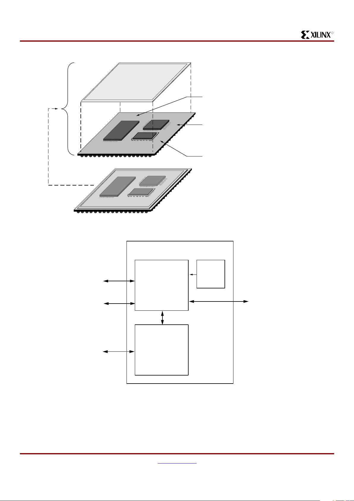
capacity FPGA systems. As shown in Figure 1, the System
ACE MPM solution is a multi-package module that includes
the System ACE MPM controller, a configuration PROM,
and an AMD Flash Memory.
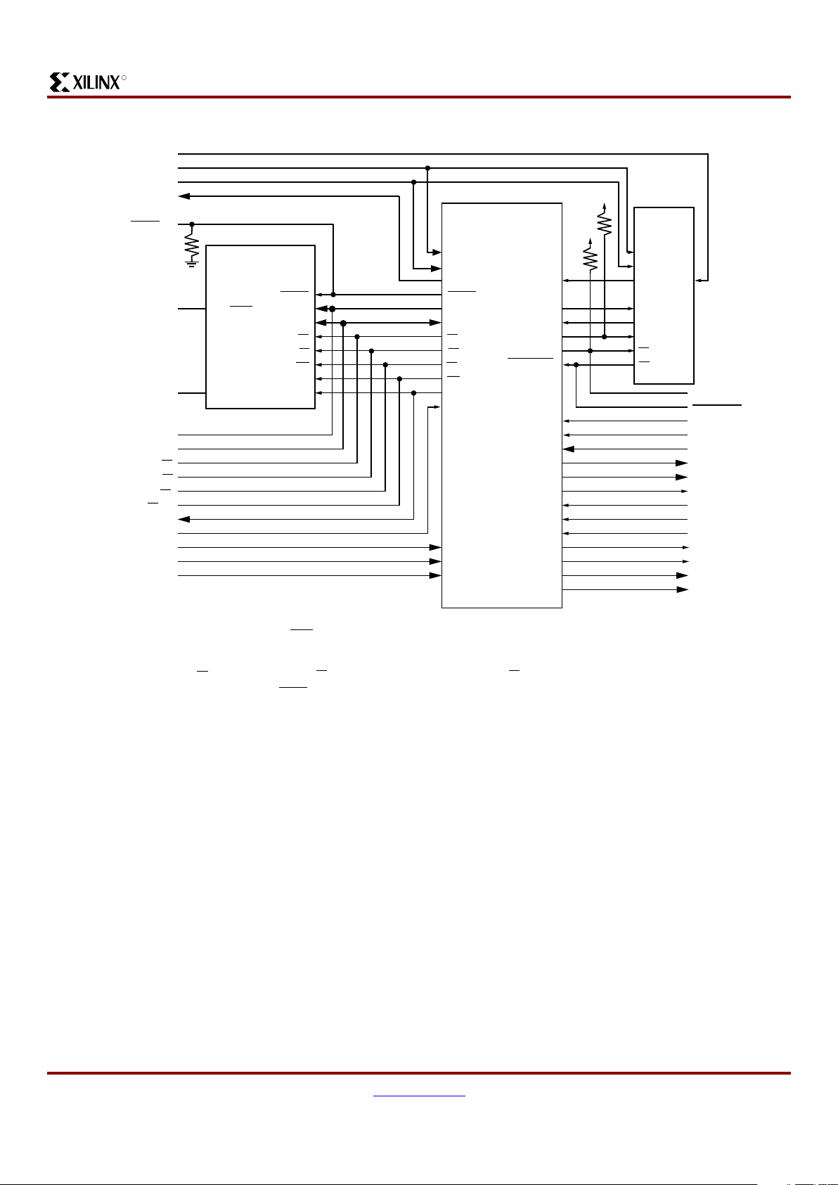
The System ACE MPM has four major interfaces. (See
Figure 2.) The boundary scan JT A G interface is prov ided for
boundary scan test and boundary-scan-based Flash memory programming. The system control interface provides an
input for the system clock, design set selection pins, system
configuration control signals, and system configuration status signals.
The native Flash memory interface provides direct read and
write access to the Flash memory unit. The target FPGA
interface provides the signals to configure target FPGAs via
the Slave-Serial, concurrent Slave-Serial, or SelectMAP
configuration modes.
Separate power pins provide voltage compatibility control
for the target FPGA configuration interfac e and for the system control/status interface.
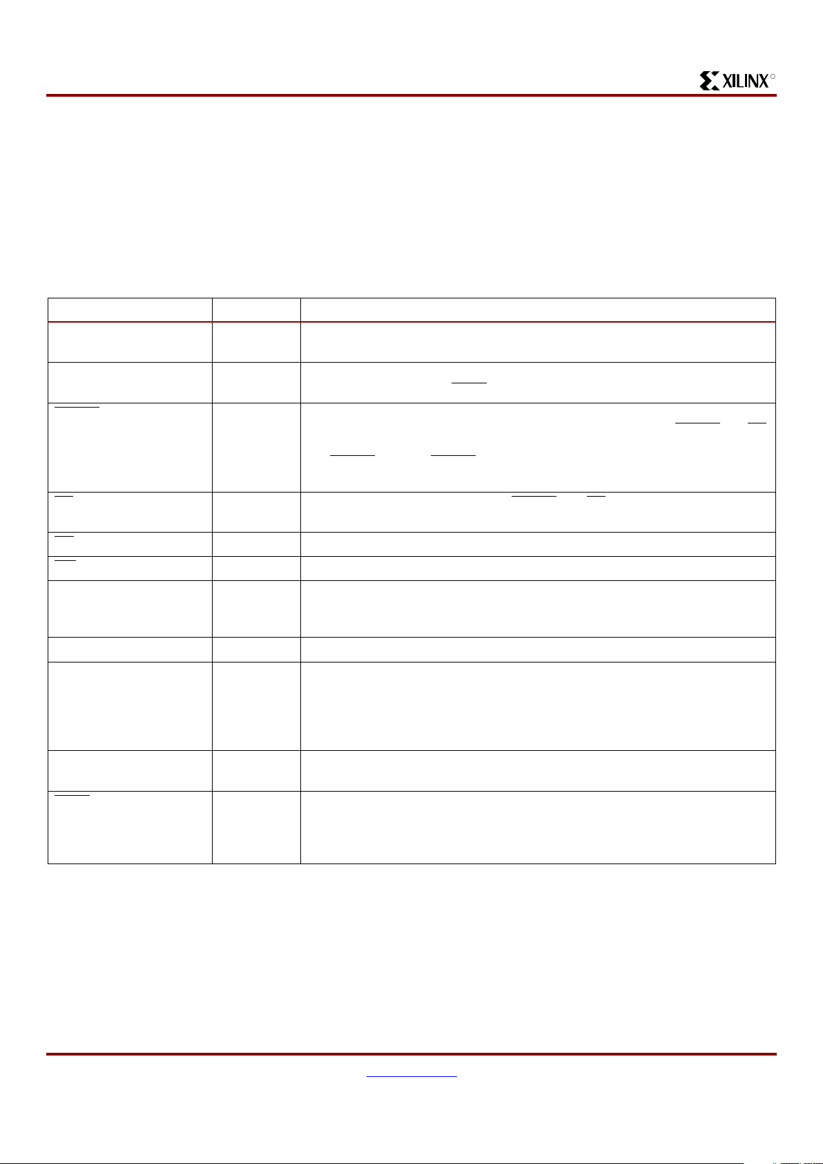
See Figure 3 for a complete view of the components and
schematic of the signals in the System ACE MPM.
0
System ACE MPM Solution
DS087 (v1.0) September 25, 2001
00
Advance Product Specification
R
Page 2
System ACE MPM Solution
2 www.xilinx.com DS087 (v1.0) September 25, 2001
1-800-255-7778 Advance Product Specification
R
Figure 1: System ACE MPM Assembly
16/32/64 Mbit AMD Flash Memory
Package: 48 pin TSOP
Dimensions: 20 x 12 x 1.2 mm
PROM XC18V01
Package: VQ44
Dimensions: 12 x 12 x 1.2 mm
Virtex XCV50E Configuration Controller
Package: CS144
Dimensions: 12 x 12 x 1.2 mm
Metal Lid
MPM BGA Module
System ACE MPM BG388
Complete Assembly
Dimensions: 35 x 35 x 2.7 mm
DS087_01_081501
Figure 2: System ACE MPM Interfaces
System ACE MPM
PROM
Slave-Serial
or SelectMAP
AMD
Flash
Memory
Boundary
Scan
Interface
System
Control
Interface
Native
Flash
Memory
XCV50E
Configuration
Controller
Target
FPGA
Interface
ds087_02_091001
Page 3
System ACE MPM So lution
DS087 (v1.0) September 25, 2001 www.xilinx.com 3
Advance Product Specification 1-800-255-7778
R
Figure 3: System ACE MPM schematic
AMD Flash
V
IO
/BYTE *
2
ACC *
4
RESET
A0-A21 *
1
DQ0-DQ15
OE
CE
WE
ACC/WP *
5
RY/BY *
3
TDI
TCK
TMS
TDO
RESET *
6
FLASH_IO_LEVEL*
2
ACC *
4
A0-A21 *
1
DQ0-DQ15
OE
CE
WE
WP *
5
RY/BY *
3
FCM_ENABLE
FLASH_VCCO
CFG_VCCO
CTRL_VCCO
XCV50E
TDI
CCLK
DIN
INIT
DONE
PROGRAM
SYSRESET
SYSCLK
BITSTRSEL[0-2]
STATUS[0-3]
CFG_MODE[0-2]
CFG_CLK
CFG_BUSY
CFG_INIT
CFG_DONE
CFG_PROG
CFG_WRITE
CFG_CS[0-3]
CFG_DATA[0-7]
TCK
TMS
TDO
RESET
A0-A21 *
1
DQ0-DQ15
OE
CE
WE
WP *
5
RY/BY *
3
FCM_ENABLE
VCCO
2,3,4,5
VCCO
6,7
VCCO
0,1
4.7k
*1
A21 for XCCACEM64 only; A20 for XCCACEM32 and XCCACEM64 only.
*2
V
IO
for XCCACEM64; BYTE for XCCACEM16 and XCCACE32.
*3
XCCACEM16 and XCCACEM32 only.
*4
XCCACEM64 only.
*5 WP on XCCACEM64; ACC/WP on XCCACEM32. Do not apply V to ACC/WP.
*6
Do not apply V
ID
to RESET.
XC18V01
TCK
TMS
TDO
CLK
D0
OE/Reset
CE
CF
TDI
300
4.7k
3.3v
3.3v
GND
System ACE MPM
DEVRDY
FCMRESET
SYSRESET
SYSCLK
BITSTRSEL[0-2]
STATUS[0-3]
CFG_MODE[0-2]
CFG_CLK
CFG_BUSY
CFG_INIT
CFG_DONE
CFG_PROG
CFG_WRITE
CFG_CS[0-3]
CFG_DATA[0-7]
DS087_03_091701
HH
Page 4
System ACE MPM Solution
4 www.xilinx.com DS087 (v1.0) September 25, 2001
1-800-255-7778 Advance Product Specification
R
Pin Descriptions
This section provides native Flash interface, Boundary
Scan, and target FPGA configuration pinout information.
Native Flash Interface Pins
All of the native Flash memory pins are routed to pins on the
System ACE MPM ball-grid-array. Thus, the Flash memory
is available to the sy stem for direct read and write access
with a few restrictions. See Note 1 and Table 1 for descriptions of the restrictions.
Notes:
1. All of the native Flash memory interface pins are connected to
the System ACE MPM controller (except where explicitly
noted in the pin description). The FCM_ENABLE pin must be
held Low to externally access the Flash memory without
contention with the System ACE MPM controller.
Boundary Scan Pins
The System ACE MPM controller (Virtex-E XCV50E) and
the System ACE MPM controller PROM (XC18V01) are
both IEEE Standard 1149.1 compatible devices. The System ACE MPM connects these devices into an internal scan
chain comprised of the XC18V01 device followed by the
XCV50E device. The internal scan chain is accessible
through the boundary scan test access port (TAP) on the
BG388 package. See Table 2.
Table 1: Native Flash Memory Interface Pins
Pin Name Pin Type Description
A0-A21 I/O Flash memory address bus. A21 exists on the XCCACEM64 only. A20 exists
on the XCCACEM32 and XCCACEM64 only.
DQ0-DQ15 I/O Flash memory data bus. DQ15 becomes the A-1 pin in the XCCACEM16 and
XCCACEM32 when the BYTE
mode is active.
RESET
I/O Flash memory hardware reset. When asserted, all Flash operations are
immediately terminated and Flash is reset to read mode. When RESET
and CE
are held High, the Flash memory is put into standby mode. Do not apply V
ID
to
the RESET
pin. The RESET is connected to the System ACE MPM controller
that has a maximum tolerance of 3.6V.
CE
I/O Flash memory chip enable. When RESET and CE are held High, the Flash
memory is put into standby mode.
OE
I/O Flash memory output enable.
WE
I/O Flash memory write enable.
RY/BY Output Flash memory ready/busy signal. Open-drain output. When Low, the RD/BY
signal indicates that the Flash is actively erasing, programming, or resetting.
XCCACEM16 and XCCACEM32 only.
WP I/O Flash memory hardware write protect.
ACC Input Flash memory accelerated mode pin. Do not apply V
HH
to the XCCACEM32
WP/ACC pin. The XCCACEM32 WP/ACC pin is connected to the System ACE
MPM controller that has a maximum tolerance of 3.6V. The XCCACEM64 A CC
pin is independent of the rest of the System ACE MPM and may be used to put
the Flash memory into accelerated program operation.
FLASH_IO_LEVEL Input Flash memory V
IO
pin on the XCCACEM64 only. This pin must be connected
to 3.3V for compatibility with the System ACE MPM controller.
BYTE
Input Flash memory byte-wide data bus mode. XCCACEM16 and XCCACEM32
only . This pin must be connected to 3.3V for compatibility with the System ACE
MPM controller and thus only the 16-bit, word mode is av ailab l e for accessing
the Flash memory in the system.
Page 5

System ACE MPM So lution
DS087 (v1.0) September 25, 2001 www.xilinx.com 5
Advance Product Specification 1-800-255-7778
R
Target FPGA Configuration Pins
Table 3 provides target FPGA configuration pins.
Table 2: IEEE 1149.1 Boundary Scan Pins
Pin Name Pin Type Description
TCK Input IEEE 1149.1 test clock pin. The System ACE MPM TCK pin is connected to the
XCV50E and XC18V01 TCK pins. By default, the XCV50E has an internal
pull-up resistor on its TCK pin.
TMS Input IEEE 1149.1 test mode select pin. The System ACE MPM TMS pin is
connected to the XCV50E and XC18V01 TMS pins which have internal pull-up
resistors.
TDI Input IEEE 1149.1 test data input pin. The System ACE MPM TDI is connected to
the XC18V01 TDI pin which has an internal pull-up resistor.
TDO Output IEEE 1149.1 test data output pin. The System A CE MPM TDO pin is connected
to the XCV50E TDO pin which by default has an internal pull-up resistor.
Table 3: Target FPGA Configuration Pins
Pin Name Pin Type Description
CFG_DATA[0] Output F or Sla ve-Serial configuration mode , CFG_D ATA[0] is the serial data signal for
Serial-Slave Chain 0 and is connected to DIN of the first FPGA in the
Slave-Serial Chain 0. F or Slave-SelectMAP configuration m ode, CFG_DAT A [0]
is the data bit 0 on the SelectMAP bus and is connected to D0 on all target
FPGAs.
CFG_DATA[1] Output F or Sla ve-Serial configuration mode , CFG_D ATA[1] is the serial data signal for
Serial-Slave Chain 1 and is connected to DIN of the first FPGA in the
Slave-Serial Chain 1. F or Slave-SelectMAP configuration m ode, CFG_DAT A [1]
is the data bit 1 on the SelectMAP bus and is connected to D1 on all target
FPGAs.
CFG_DATA[2] Output F or Sla ve-Serial configuration mode , CFG_D ATA[2] is the serial data signal for
Serial-Slave Chain 2 and is connected to DIN of the first FPGA in the
Slave-Serial Chain 2. F or Slave-SelectMAP configuration m ode, CFG_DAT A [2]
is the data bit 2 on the SelectMAP bus and is connected to D2 on all target
FPGAs.
CFG_DATA[3] Output F or Sla ve-Serial configuration mode , CFG_D ATA[3] is the serial data signal for
Serial-Slave Chain 3 and is connected to DIN of the first FPGA in the
Slave-Serial Chain 3. F or Slave-SelectMAP configuration m ode, CFG_DAT A [3]
is the data bit 3 on the SelectMAP bus and is connected to D3 on all target
FPGAs.
CFG_DATA[4] Output F or Sla ve-Serial configuration mode , CFG_D ATA[4] is the serial data signal for
Serial-Slave Chain 4 and is connected to DIN of the first FPGA in the
Slave-Serial Chain 4. F or Slave-SelectMAP configuration m ode, CFG_DAT A [4]
is the data bit 4 on the SelectMAP bus and is connected to D4 on all target
FPGAs.
CFG_DATA[5] Output F or Sla ve-Serial configuration mode , CFG_D ATA[5] is the serial data signal for
Serial-Slave Chain 5 and is connected to DIN of the first FPGA in the
Slave-Serial Chain 5. F or Slave-SelectMAP configuration m ode, CFG_DAT A [5]
is the data bit 5 on the SelectMAP bus and is connected to D5 on all target
FPGAs.
Page 6
System ACE MPM Solution
6 www.xilinx.com DS087 (v1.0) September 25, 2001
1-800-255-7778 Advance Product Specification
R
Pin Name Pin Type Description
CFG_DATA[6] Output F or Sla ve-Serial configuration mode , CFG_D ATA[6] is the serial data signal for
Serial-Slave Chain 6 and is connected to DIN of the first FPGA in the
Slave-Serial Chain 6. F or Slave-SelectMAP configuration m ode, CFG_DAT A [6]
is the data bit 6 on the SelectMAP bus and is connected to D6 on all target
FPGAs.
CFG_DATA[7] Output F or Sla ve-Serial configuration mode , CFG_D ATA[7] is the serial data signal for
Serial-Slave Chain 7 and is connected to DIN of the first FPGA in the
Slave-Serial Chain 7. F or Slave-SelectMAP configuration m ode, CFG_DAT A [7]
is the data bit 7 on the SelectMAP bus and is connected to D7 on all target
FPGAs.
CFG_MODE[0] Output The CFG_MODE pins set the configuration mode on the target FPGAs.
Connect CFG_MODE[0] to the M0 pin on all target FPGAs.
CFG_MODE[1] Output The CFG_MODE pins set the configuration mode on the target FPGAs.
Connect CFG_MODE[1] to the M1 pin on all target FPGAs.
CFG_MODE[2] Output The CFG_MODE pins set the configuration mode on the target FPGAs.
Connect CFG_MODE[2] to the M2 pin on all target FPGAs.
CFG_CCLK Output CFG_CCLK is the configuration clock source for the target FPGAs. The
CFG_CCLK is derived from the SYSCLK. The CFG_CCLK frequency is half
the SYSCLK frequency. Connect CFG_CCLK to the CCLK pin on all target
FPGAs.
CFG_PROG
Output CFG_PROG is pulsed Low at the beginning of the configuration download to
reset the configuration state of the target FPGAs. CFG_PROG
is connected to
the PROG_B pin on all target FPGAs.
CFG_INIT Input Target FPGA INIT monitor pin. At the start of the configuration process, the
System ACE MPM controller waits for INIT to go High bef ore initiating deliv ery
of configuration data through the CFG_DATA pins. CFG_INIT is connected to
the INIT pin on all target FPGAs.
CFG_BUSY Input When CFG_B USY is High, the CFG_DAT A outputs are held. If the target FP GA
configuration mode is Slave-SelectMAP and if the CFG_CCLK is greater than
50 MHz, connect the CFG_BUSY pin to the BUSY pin on all target FPGAs.
Otherwise, pull-down the CFG_BUSY pin to GND.
CFG_DONE Input CFG_DONE monitors the DONE status on all target FPGAs. Connect the
CFG_DONE to the DONE pin on all target FPGAs. DONE must be pulled High
with an external 330-8 pull-up resistor. The BitGen option DriveDONE should
be left in the default “NO” setting when generating bitstreams for Xilinx FPGAs.
CFG_WRITE
Output Slave-SelectMAP write-enable pin. Connect the CFG_WRITE pin to the
RDWR_B pin on all target FPGAs.
CFG_CS[0]
Output S lav e-SelectMAP chip-enab le f or target FPGA 0. Connect the CFG_CS[0] pin
to the CS_B pin on target FPGA 0.
CFG_CS[1]
Output S lav e-SelectMAP chip-enab le f or target FPGA 1. Connect the CFG_CS[1] pin
to the CS_B pin on target FPGA 1.
CFG_CS[2]
Output S lav e-SelectMAP chip-enab le f or target FPGA 2. Connect the CFG_CS[2] pin
to the CS_B pin on target FPGA 2.
CFG_CS[3]
Output S lav e-SelectMAP chip-enab le f or target FPGA 3. Connect the CFG_CS[3] pin
to the CS_B pin on target FPGA 3.
Table 3: Target FPGA Configuration Pins (Continued)
Page 7
System ACE MPM So lution
DS087 (v1.0) September 25, 2001 www.xilinx.com 7
Advance Product Specification 1-800-255-7778
R
System Control and Status Pins
Table 4 provides system control and status pins.
Power and Ground Pins
The System ACE MPM requires at least two power supplies: 1.8V supplies power to the System ACE MPM configuration controller (an XCV50E) core; and 3.3V supplies
power to the Flash memory and configuration controller
PROM (an XC18V01). Additional power supplies may be
required for the output voltage compatibility pins:
FLASH_VCCO, CFG_VCCO, and CTRL_VCCO. See
Figure 4 and Table 5 for a description of the System ACE
MPM power pins.
Table 4: System Control and Status Pins
Pin Name Pin Type Description
FCM_ENABLE Input System ACE MPM controller enable. When this pin is held Low, all of the
System ACE MPM controller (XCV50E) pins tied to the Flash memory are
3-stated allowing external peripherals access to Flash memory without
contention.
FCMRESET
Input System ACE MPM FPGA reset pin. The FCMRESET pin is connected to the
XCV50E PRO GR AM
pin. Applying a Low pulse to the FCMRESET resets the
XCV50E and forces the XCV50E to reconfigure itself from the XC18V01
PROM. (The XCV50E automatically configures itself from the XC18V01 PROM
at power-up.)
DEVRDY Output System ACE MPM FPGA DONE pin. The DEVRDY pin is connected to the
XCV50E DONE pin. When DEVRDY is High, the XCV50E is configured and
ready for operation.
SYSCLK Input SYSCLK is the system clock input for the System ACE MPM control logic.
SYSRESET Input Hold SYSRESET High for at least 10 SYSCLK cycles to reset the System ACE
MPM control logic. Upon release from the reset condition, the System ACE
MPM initiates the download procedure to the target FPGAs.
BITSTRSEL[2-0] Input The BITSTRSEL pins determine which of the eight configuration data streams
to download to the target FPGA.
STATUS[3-0] Output The STATUS pins indicate the status of the System ACE MPM control logic.
Figure 4: Power Pins
DS087_04_090601
System ACE
MPM
CFG_VCCO
Configuration
Signals
VCCint1
VCCint2
FLASH_VCCO
CTRL_VCCO
Control
Signals
Slave-Serial
or
Slave-SelectMAP
Control
Circuits
BITSTRSEL[0-2]
SYSCLK
SYSRESET
1.8v
3.3v
CFG_VCCO
Compatible with
Target FPGAs
CTRL_VCCO
Compatible with
Control Circuits
System Signals
XILINX
Virtex-II
XILINX
Spartan-II
XILINX
Virtex-II
XILINX
Virtex-II
Page 8
System ACE MPM Solution
8 www.xilinx.com DS087 (v1.0) September 25, 2001
1-800-255-7778 Advance Product Specification
R
Pinout
Table 6 provides System ACE MPM pinout. Unlisted BGA sites are no connects.
Table 5: Power and Ground Pins
Pin Name Pin Type Description
VCC
INT1
Power 1.8V power supply pins for the Virtex-E XCV50E configuration controller cor e .
The 1.8V power supply should rise prior to or simultaneously to the
FLASH_VCCO, CTRL_VCCO, and CFG_VCCO power supplies.Otherwise,
the XCV50E device might draw excessive current.
VCC
INT2
Power 3.3V power supply pins for the AMD Flash memory and the XC18V01 PROM.
FLASH_VCCO Pow er 3.3V pow er supply for the I/O banks connecting the Virtex-E XCV50E controller
to the AMD Flash memory.
CFG_VCCO Pow er Configurable power supply f or the I/O banks on the target FPGA configuration
interface. Connect this power pin to a voltage that is compatible with the target
FPGA configuration pins.
CTRL_VCCO Pow er Configurable power supply for the I/O banks on the system interface . Connect
this power pin to a v oltage that is compatible with the system control a nd status
monitor signals.
GND Ground Ground.
Table 6: System ACE MPM Pinout
Pin Name XCCACEM16-BG388I XCCACEM32-BG388I XCCACEM64-BG388I
A0 AF8 AF8 AF8
A1 AF4 AF4 AF4
A2 AF3 AF3 AF3
A3 AF2 AF2 AF2
A4 AE4 AE4 AE4
A5 AE3 AE3 AE3
A6 AE1 AE1 AE1
A7 AD2 AD2 AD2
A8 W1 W1 W1
A9 W2 W2 W2
A10V1V1V1
A11V2V2V2
A12 U1U1U1
A13 U2U2U2
A14 T1 T1 T1
A15 T2 T2 T2
A16 R25 R25 R25
A17 AD1 AD1 AD1
A18 AC2 AC2 AC2
Page 9

System ACE MPM So lution
DS087 (v1.0) September 25, 2001 www.xilinx.com 9
Advance Product Specification 1-800-255-7778
R
Pin Name XCCACEM16-BG388I XCCACEM32-BG388I XCCACEM64-BG388I
A19Y1Y1AC1
A20 n/a Y2 Y2
A21 n/a n/a Y1
DQ0 AD26 AD26 AD26
DQ1 AC25 AC25 AC25
DQ2 AB26 AB26 AB26
DQ3 AA26 AA26 AA26
DQ4 Y26 Y26 Y26
DQ5 W26 W26 W26
DQ6 U26 U26 U26
DQ7 T26 T26 T26
DQ8 AD25 AD25 AD25
DQ9 AC26 AC26 AC26
DQ10 AB25 AB25 AB25
DQ11 AA25 AA25 AA25
DQ12 Y25 Y25 Y25
DQ13 W25 W25 W25
DQ14 U25 U25 U25
DQ15 T25 T25 T25
RESET AA2 AA2 AA2
CE AE23 AE23 AE23
OE AE26 AE26 AE26
WE AA1 AA1 AA1
RY/BY AC1 AC1 n/a
WP n/a AB2 AB2
ACC n/a n/a AB1
FLASH_IO_LEVEL R26 R26 R26
FCM_ENABLE B7 B7 B7
FCMRESET K26 K26 K26
DEVRDY N26 N26 N26
TCK G26 G26 G26
TMSA3A3A3
TDI F26 F26 F26
TDO A15 A15 A15
SYSCLK A9 A9 A9
SYSRESET B8 B8 B8
Table 6: System ACE MPM Pinout (Continued)
Page 10

System ACE MPM Solution
10 www.xilinx.com DS087 (v1.0) September 25, 2001
1-800-255-7778 Advance Product Specification
R
Pin Name XCCACEM16-BG388I XCCACEM32-BG388I XCCACEM64-BG388I
BITSTRSEL[0] A6 A6 A6
BITSTRSEL[1] B5 B5 B5
BITSTRSEL[2] A5 A5 A5
STATUS[0] A10 A10 A10
STATUS[1]B9B9B9
STATUS[2]B6B6B6
STATUS[3]A7A7A7
CFG_DATA[0] J2 J2 J2
CFG_DATA[1] J1 J1 J1
CFG_DATA[2] H3 H3 H3
CFG_DATA[3] G2 G2 G2
CFG_DATA[4] H2 H2 H2
CFG_DATA[5] H1 H1 H1
CFG_DATA[6] J3 J3 J3
CFG_DATA[7] G3 G3 G3
CFG_MODE[0] H26 H26 H26
CFG_MODE[1] E1 E1 E1
CFG_MODE[2] F2 F2 F2
CFG_CCLK K1 K1 K1
CFG_BUSY G1 G1 G1
CFG_INIT K3 K3 K3
CFG_PROG K2 K2 K2
CFG_DONE B3 B3 B3
CFG_WRITE L1 L1 L1
CFG_CS[0] B1 B1 B1
CFG_CS[1] D1 D1 D1
CFG_CS[2] C1 C1 C1
CFG_CS[3] A1 A1 A1
CTRL_VCCO A4, A16, A11 A4, A16, A 1 1 A4, A16, A11
CFG_VCCO M1, B4, F1 M1, B4, F1 M1, B4, F1
FLASH_VCCO B14, J26, L26, AF13, N1,
AF9
B14, J26, L26, AF13, N1,
AF9
B14, J26, L26, AF13, N1,
AF9
VCCint1 C3, C7, C8, C9, C10, D6,
D7, D8,
D13, D14, E4, F4, K4, L2,
M2, M3
C3, C7, C8, C9, C10, D6,
D7, D8,
D13, D14, E4, F4, K4, L2,
M2, M3
C3, C7, C8, C9, C10, D6,
D7, D8,
D13, D14, E4, F4, K4, L2,
M2, M3
Table 6: System ACE MPM Pinout (Continued)
Page 11

System ACE MPM So lution
DS087 (v1.0) September 25, 2001 www.xilinx.com 11
Advance Product Specification 1-800-255-7778
R
Configuration Overview
The System ACE MPM is engineered for high -speed configuration of high-density FPGAs. Multiple configuration
modes are supported to target FPGAs including Concurrent
Slave-Serial mode, Sla ve-SelectMAP mode , and Slav e-P arallel mode. The System A CE MPM handles storage of up to
eight separate configuration data sets. Each data set can be
optionally compressed to reduce the overall storage
requirements. One default data set is automatically downloaded to the target FPGAs at system power-up. An y one of
the eight data sets can be selected to reconfigure the target
FPGAs at any time during system operation.
Configuration Modes
The System ACE MPM supports high-speed FPGA configuration via the Slave-Serial or Slave-SelectMAP configuration modes.
The System ACE MPM solution is a pre-engineered storage
and delivery system with direct support for the high-density
and high-speed configuration needs of the Virtex-II family.
For example, the System ACE MPM can configure a Virtex-II XC2V6000, which requires 19,759,968 configuration
bits, via Slave-Serial mode in 300 milliseconds and via
Slave-SelectMAP mode in 130 milliseconds. In fact, the
System ACE MPM can configure two XC2V6000 devices
concurrently via Slave-Serial mode in 300 milliseconds.See
Table 7 for maximum configuration bit r ates . S ee Table 8 for
FPGA configuration compatibility and cross-reference.
SeeTable 9 for System ACE MPM and FPGA configuration
signal cross-reference.
Pin Name XCCACEM16-BG388I XCCACEM32-BG388I XCCACEM64-BG388I
VCCint2 AA23, AB4, AB23, AC4,
AC11, AC12, AC13, AC18,
AC19, AC20, D17, D18,
D21, D22, D23, E23, H23,
J23, N23, P23, R4, T4, U4,
V26, Y23
AA23, AB4, AB23, AC4,
AC11, AC12, AC13, AC18,
AC19, AC20, D17, D18,
D21, D22, D23, E23, H23,
J23, N23, P23, R4, T4, U4,
V26, Y23
AA23, AB4, AB23, AC4,
AC11, AC12, AC13, AC18,
AC19, AC20, D17, D18,
D21, D22, D23, E23, H23,
J23, N23, P23, R4, T4, U4,
V26, Y23
GND A2, A8, A26, AA3, AB24,
AD16, AD22, AE2, AE11,
AE12, AE18, AE22, AE25,
AF1, AF26, B15, B19, B22,
B25, D4, D9, D10, D11,
F23, G4, H25, J4, K23, L4,
L11, L12, L13, L14, L15,
L16, M4, M11, M12, M13,
M14, M15, M16, M23, N11,
N12, N13, N14, N15, N16,
P2, P11, P12, P13, P14,
P15, P16, R1, R11, R12,
R13, R14, R15, R16, R23,
T11, T12, T13, T14, T15,
T16, T23, V25
A2, A8, A26, AA3, AB24,
AD16, AD22, AE2, AE11,
AE12, AE18, AE22, AE25,
AF1, AF26, B15, B19, B22,
B25, D4, D9, D10, D11,
F23, G4, H25, J4, K23, L4,
L11, L12, L13, L14, L15,
L16, M4, M11, M12, M13,
M14, M15, M16, M23, N11,
N12, N13, N14, N15, N16,
P2, P11, P12, P13, P14,
P15, P16, R1, R11, R12,
R13, R14, R15, R16, R23,
T11, T12, T13, T14, T15,
T16, T23, V25
Table 6: System ACE MPM Pinout (Continued)
Page 12

System ACE MPM Solution
12 www.xilinx.com DS087 (v1.0) September 25, 2001
1-800-255-7778 Advance Product Specification
R
Table 7: Maximum Configuration Bit Rates
Configuration
Mode
Maximum System
Clock Rate
(SYSCLK)
Maximum
Configuration Clock
(CFG_CCLK) Rate
(at Max SYSCLK
Rate)
Average
Configuration Clock
Rate (at Max
SYSCLK Rate)
Maximum Average
Combined Configuration
Bit Rate
Slave-SelectMAP 133 MHz 44 MHz 19 MHz‘ 152 Mb/s
Slave-Serial 133 MHz 66 MHz 66 MHz 66 Mb/s
2 Concurrent
Slave-Serial
Chains
133 MHz 66 MHz 66 MHz 133 Mb/s
(66 Mb/s per chain)
3 - 4 Concurrent
Slave-Serial
Chains
133 MHz 66 MHz 38 MHz 152 Mb/s
(38 Mb/s per chain)
5 - 8 Concurrent
Slave-Serial
Chains
133 MHz 66 MHz 19 MHz 152 Mb/s
(19 Mb/s per chain)
Table 8: FPGA Configuration Compatibility and Cross-Reference
General
Description Clock Source
Data
Path Delivery Method Virtex-II
Virtex
Virtex-E Spartan-II
Serial
Configuration
Mode
External 1-bit Cascade through
FPGAs in daisy-chain
style
Slave-Serial Slave-Serial Slave-Serial
Parallel
Configuration
Mode
External 8-bits Chip-selected device
on configuration data
bus
Slave-
SelectMAP
SelectMAP Slave-Parallel
Table 9: System ACE MPM and FPGA Configuration Signal Cross-Reference
FPGA Configuration
Signal System ACE MPM Virtex-II
Virtex/
Virtex-E Spartan-II
Configuration Mode CFG_MODE[2:0] M2, M1, M0 M2, M1, M0 M2, M1, M0
Configuration Clock CFG_CLK CCLK CCLK CCLK
Configuration Data CFG_DATA[7:0] D7, D6, D5,
D4, D3, D2,
D1, DIN/D0
D7, D6, D5,
D4, D3, D2,
D1, DIN/D0
D7, D6, D5,
D4, D3, D2,
D1, DIN/D0
Configuration Reset CFG_PROG PROG_B PROGRAM PROGRAM
Configuration CFG_INIT INIT_B INIT INIT
Configuration Busy CFG_BUSY BUSY BUSY BUSY
Page 13

System ACE MPM So lution
DS087 (v1.0) September 25, 2001 www.xilinx.com 13
Advance Product Specification 1-800-255-7778
R
Slave-Serial
Similar to the Xilinx PROM solution, the System ACE MPM
is a single package solution that supports the configuration
of a single, cascaded chain of Slave-Serial FPGAs. With the
maximum configuration clock rate of 66 MHz, the System
ACE MPM is twice as fast as the neares t Xilinx PROM configuration solution in the Slave-Serial mode.
The System ACE MPM has additional support for concurrently configuring multiple chains of Slave-Serial FPGAs.
Multiple data output pins on the System ACE MPM can concurrently supply bitstreams for two to eight Slave-Serial
FPGA chains. Although each Slav e-Serial chain has a maximum configuration clock rate of 66 MHz, the maximum bit
delivery rate of 66 Mb/s is maintained across all concurrent
Slave-Serial FPGA chains up to the cumulative maximum of
152 Mb/s. (152 Mb/s is the maximum read rate from the
AMD Flash memory in the System ACE MPM.)
In the Concurrent Slave-Serial configuration mode, the bitstreams for the individual Slave-Serial chains are interleaved and optimized for concurrent configuration of two,
four, or eight Slave-Serial FPGA chains. Configuration time
and storage requirements are optimal when the data strea m
sizes are equivalent across all concurrent Slave-Serial
FPGA chains.
The connectivity between the System ACE MPM and
Slave-Serial FPGA chain is similar to the connectivity
between a Xilinx PROM and a Slave-Serial FPGA chain. All
configuration signals between Concurrent Slave-Serial
FPGA chains are common except that data for the first
chain originates from the System ACE MPM CFG_DATA[0]
pin, the data for the second chain originates from the
System ACE MPM CFG_DATA[1] pin, etc. See Figure 5 fo r
a schematic of the Slave-Serial configuration signal connections, and see Table 10 for a list of the Slave-Serial configu-
ration signals. The voltage compatibility for the System ACE
MPM configuration interface is configurable via the
CFG_VCCO pin. CFG_VCCO should be connected to a
voltage level that is compatib le with the target FPGAs. Typically, CFG_VCCO is connected to either 3.3V or 2.5V. Consult the target FPGA data sheet for an appropriate
configuration signal voltage level.
Identical configuration of multiple target FPGAs from one
bitstream can be achieved through the appropr iate configuration signal connections. Figure 7 shows an example of
two FPGAs that are identically configured from a single bitstream. Table 10 provides the Slave-Serial configuration
signals.
Configuration Done CFG_DONE DONE DONE DONE
SelectMAP/Slave-
Parallel Bus Read/Write
Signal
CFG_WRITE RDWR_B WRITE WRITE
SelectMAP/SlaveParallel Bus Chip Select
Signal
CFG_CS[3:0] CS_B CS CS
Table 9: System ACE MPM and FPGA Configuration Signal Cross-Reference
FPGA Configuration
Signal System ACE MPM Virtex-II
Virtex/
Virtex-E Spartan-II
Page 14

System ACE MPM Solution
14 www.xilinx.com DS087 (v1.0) September 25, 2001
1-800-255-7778 Advance Product Specification
R
Figure 5: System ACE MPM Configuration Modes
Chip Selects for up to 4 Devices
CS0 CS1 CS2 CS3
AMD
Flash
Memory
FPGA FPGA FPGA FPGA
FPGA FPGA FPGA
FPGA
FPGA FPGA
FPGA
FPGA FPGA
System ACE
Configuration
Controller
AMD
Flash
Memory
System ACE
Configuration
Controller
AMD
Flash
Memory
System ACE
Configuration
Controller
152 Mb/s
SelectMAP bus
66 Mb/s
Serial data stream
Up to 152 Mb/s
Serial data stream
2 to 8 chains
66Mb/s per chain
Serial data stream
.
.
.
ds087_05_091701
Configuration Modes
SelectMAP
Slave-Serial
Concurrent Slave-Serial
Figure 6: Slave-Serial Configuration Mode
System ACE MPM
CFG_VCCO
CFG_DATA[0-7] *
3
CFG_MODE[2]
CFG_MODE[1]
CFG_MODE[0]
CFG_CCLK
CFG_INIT
CFG_DONE
CFG_PROG
BUSY
FPGA
DOUTD0
M2
M1
M0
CCLK
INIT_B
DONE
PROG_B
DOUTD0
M2
M1
M0
CCLK
INIT_B
DONE
PROG_B
To Chain0
Cascaded
FPGAs
CFG_DATA[1-7] *
3
To Concurrent Slave-Serial
FPGA Chains (1-7)
(Chain 0, Device 0)
FPGA
(Chain 0, Device 1)
*1 Supply voltage to CFG_VCCO that is compatible with the FPGA configuration pins.
*2 Only /WP on XCCACEM16; Combined ACC/WP on XCCACEM32; Separate /WP and ACC on XCCACEM64.
*3 Use CFG_DATA[0] for systems with one slave-serial chain; Use CFG_DATA[0-1] for systems with two concurrent slave-serial
chains; Use CFG_DATA[0-3] for systems with four concurrent slave-serial chains; Use CFG_DATA[0-7] for systems with eight
concurrent slave-serial chains.
FLASH_IO_LEVEL
WP *
2
ACC *
2
FCM_ENABLE
SYSCLK
BITSTRSEL[0-2]
STATUS[0-3]
SYSRESET
CLK Source
BITSTRSEL[0-2]
330
CFG_DATA[0]
4.7k
4.7k
3.3v
4.7 k
CFG_VCCO *
1
4.7 k
DS087_05_091201
Page 15

System ACE MPM So lution
DS087 (v1.0) September 25, 2001 www.xilinx.com 15
Advance Product Specification 1-800-255-7778
R
Figure 7: Example Slave-Serial Configuration for Identically Configured Xilinx FPGAs
DS087_07_091701
CFG_VCCO
CFG_DATA[0]
CFG_MODE[2]
CFG_MODE[1]
CFG_MODE[0]
CFG_CCLK
CFG_INIT
CFG_DONE
CFG_PROG
BUSY
FPGA
D0
M2
M1
M0
CCLK
INIT_B
DONE
PROG_B
FPGA
D0
M2
M1
M0
CCLK
INIT_B
DONE
PROG_B
To
Identical
FPGAs
*1 Supply voltage to CFG_VCCO that is compatible with the FPGA configuration pins.
*2 Combined ACC/WP on XCCACEM32; Separate WP and ACC on XCCACEM64.
CFG_DATA[0]
CFG_DATA[0]
System ACE MPM
FLASH_IO_LEVEL
WP *
2
ACC *
2
FCM_ENABLE
SYSCLK
BITSTRSEL[0-2]
STATUS[0-3]
SYSRESET
CLK Source
BITSTRSEL[0-2]
3.3 V
4.7 k
4.7 k
330
4.7 k
4.7 k
CFG_VCCO
*
1
Table 10: Slave-Serial FPGA Configuration Signals
System ACE MPM
Single
Slave-Serial Chain
Two
Slave-Serial Chains
Four
Slave-Serial Chains
Eight
Slave-Serial Chains
CFG_MODE[0] M0 on all FPGAs M0 on all FPGAs M0 on all FPGAs M0 on all FPGAs
CFG_MODE[1] M1 on all FPGAs M1 on all FPGAs M1 on all FPGAs M1 on all FPGAs
CFG_MODE[2] M2 on all FPGAs M2 on all FPGAs M2 on all FPGAs M2 on all FPGAs
CFG_CCLK CCLK on all FPGAs CCLK on all FPGAs CCLK on all FPGAs CCLK on all FPGAs
CFG_PROG
PROG_B on all
FPGAs
PROG_B on all
FPGAs
PROG_B on all
FPGAs
PROG_B on all
FPGAs
CFG_INIT INIT_B on all FPGAs INIT_B on all FPGAs INIT_B on all FPGAs INIT_B on all FPGAs
CFG_DONE DONE on all FPGAs DONE on all FPGAs DONE on all FPGAs DONE on all FPGAs
CFG_DATA[0] DIN on first FPGA of
Chain 0
DIN on first FPGA of
Chain 0
DIN on first FPGA of
Chain 0
DIN on first FPGA of
Chain 0
CFG_DATA[1] DIN on first FPGA of
Chain 1
DIN on first FPGA of
Chain 1
DIN on first FPGA of
Chain 1
CFG_DATA[2] DIN on first FPGA of
Chain 2
DIN on first FPGA of
Chain 2
CFG_DATA[3] DIN on first FPGA of
Chain 3
DIN on first FPGA of
Chain 3
Page 16

System ACE MPM Solution
16 www.xilinx.com DS087 (v1.0) September 25, 2001
1-800-255-7778 Advance Product Specification
R
Although Table 10 lists configuration signals for only one,
two, four, or eight Slave-Serial chain systems, any number
of Slave-Serial chains from one to eight are supported in the
System ACE software. The System ACE software assigns
the data streams for each Slave-Serial chain starti ng from
CFG_DATA[0] up to CFG_DATA[N-1] where N is the number
of Slave-Serial chains in the system.
Slave-SelectMAP/Slave-Parallel
The System ACE MPM conveniently suppor ts high-speed,
sequential configuration of up to four Xilinx FPGAs via the
8-bit-wide SelectMAP configuration bus or four Spartan-II
devices via the 8-bit-wide Slave-Parallel bus. The System
ACE MPM generates a maximum configuration clock rate of
19 MHz. The maximum bit delivery rate is 152 Mb/s. (152
Mb/s is the maximum read rate from the AMD Flash memory in the System ACE MPM.)
The connectivity between the System ACE MPM and the
FPGAs on the SelectMAP bus is similar to the connectivity
between a Xilinx PROM and a Slav e-SelectMAP FPGA with
the addition of the CFG_WRITE and separate CFG_CS
(chip select) signals. All configuration signals from the System ACE MPM are common to all of the target FPGAs on
the SelectMAP bus, except that the C S_B signal of the first
FPGA must be connected to the System ACE MPM
CFG_CS[0] pin, and the CS_B signal of the second FPGA
must be connected to the System ACE MPM CFG_CS[1]
pin, etc. See Figure 8 for a schematic diagram of the
Slave-SelectMAP configuration connections, and Table 11
for a list of the Slave-SelectMAP connections for up to four
target FPGAs.
The Spartan-II Slave-Parallel mode has the s ame structure
and protocol as the Slave-SelectMA P mode. Therefore, the
Slave-SelectMAP figure and table apply to the Spartan-II
Slave-P arallel mode with the appropriate signal name translations noted in Table 11
System ACE MPM
Single
Slave-Serial Chain
Two
Slave-Serial Chains
Four
Slave-Serial Chains
Eight
Slave-Serial Chains
CFG_DATA[4] DIN on first FPGA of
Chain 4
CFG_DATA[5] DIN on first FPGA of
Chain 5
CFG_DATA[6] DIN on first FPGA of
Chain 6
CFG_DATA[7] DIN on first FPGA of
Chain 7
Table 10: Slave-Serial FPGA Configuration Signals (Continued)
Page 17

System ACE MPM So lution
DS087 (v1.0) September 25, 2001 www.xilinx.com 17
Advance Product Specification 1-800-255-7778
R
.
Figure 8: Slave-SelectMAP Configuration Mode
ds087_08_91001
CFG_VCCO
CFG_DATA[7:0]
CFG_MODE[2:0]
CFG_CCLK
CFG_INIT
CFG_DONE
CFG_PROG
CFG_WRITE
BUSY
CFG_CS[0-3] *
3
FPGA
CS_B
D[7:0]
M[2:0]
CCLK
INIT_B
DONE
PROG_B
RDWR_B
BUSY
To
SelectMAP
FPGAs (2-3)
FPGA
CS_B
D[7:0]
M[2:0]
CCLK
INIT_B
DONE
PROG_B
RDWR_B
BUSY
(CFG_CS[0])
(CFG_CS[1])
CFG_CS[1]
CFG_CS[0]
*1 Supply voltage to CFG_VCCO that is compatible with the FPGA configuration pins.
*2 Combined ACC/WP on XCCACEM32; Separate /WP and ACC on XCCACEM64.
*3 Use CFG_CS[0] for systems with one slave-SelectMAP FPGA ; Use CFG_CS[0-1] for systems with two slave-
SelectMAP FPGAs; Use CFG_CS[0-2] for systems with three slave-SelectMAP FPGAs; Use CFG_CS[0-3] for
systems with four slave-SelectMAP FPGAs.
System ACE MPM
FLASH_IO_LEVEL
WP *
2
ACC *
2
FCM_ENABLE
SYSCLK
BITSTRSEL[0-2]
STATUS[0-3]
SYSRESET
CLK Source
BITSTRSEL[0-2]
3.3 V
4.7 k
4.7 k
330
4.7 k
4.7 k
CFG_VCCO *
1
Table 11: Slave-SelectMAP FPGA Configuration Signals
System ACE MPM FPGA 0 FPGA 1 FPGA 2 FPGA 3
CFG_MODE[0]M0M0M0M0
CFG_MODE[1]M1M1M1M1
CFG_MODE[2]M2M2M2M2
CFG_CCLK CCLK CCLK CCLK CCLK
CFG_PROG
PROG_B PROG_B PROG_B PROG_B
CFG_INIT INIT_B INIT_B INIT_B INIT_B
CFG_BUSY BUSY BUSY BUSY BUSY
CFG_DONE DONE DONE DONE DONE
CFG_DATA[0-7] D[0-7] D[0-7] D[0-7] D[0-7]
CFG_WRITE
RDWR_B RDWR_B RDWR_B RDWR_B
CFG_CS
[0] CS_B
CFG_CS[1] CS_B
CFG_CS[2] CS_B
CFG_CS[3] CS_B
Page 18

System ACE MPM Solution
18 www.xilinx.com DS087 (v1.0) September 25, 2001
1-800-255-7778 Advance Product Specification
R
Identical configuration of multiple target FPGAs from a single bitstream can be achieved through the appropriate connections. See Figure 9 for an example of two FPGAs that
are simultaneously configured from a single bitstream.
The System ACE software assigns bitstreams for the target
FPGAs in order, starting from the CFG_CS[0
] pin through
CFG_CS[N-1]
pin where N is the number of S lave-Select-
MAP devices in the system. N may be up to four devices.
Configuration Data
The configuration data sets for the target FPGAs are stored
in a standard, high-density Flash memory unit in the System
ACE MPM.
Data Storage
The System ACE MPM integrates a standard Flash memory
unit for storage of the configuration data sets. See Table 12.
The System ACE MPM product family offers data storage
capacity up to 64 Mb. See the Flash memory vendor’s data
sheets for additional information about the Flash memory
unit in the System ACE MPM. See Table 13 for Flash memory data sheet references.
Figure 9: Example Slave-SelectMAP Configuration for Identically Configured FPGAs
DS087_09_091001
CFG_VCCO
CFG_DATA[7:0]
CFG_MODE[2:0]
CFG_CCLK
CFG_INIT
CFG_DONE
CFG_PROG
CFG_WRITE
BUSY
CFG_CS[0]
FPGA
CS_B
D[7:0]
M[2:0]
CCLK
INIT_B
DONE
PROG_B
RDWR_B
BUSY
To
Identical
SelectMAP
FPGAs
FPGA
CS_B
D[7:0]
M[2:0]
CCLK
INIT_B
DONE
PROG_B
RDWR_B
BUSY
CFG_CS[0]CFG_CS[0]
System ACE MPM
*
1
Supply voltage to CFG_VCCO that is compatible with the FPGA configuration pins.
*
2
Combined ACC/WP on XCCACEM32; Separate /WP and ACC on XCCACEM64.
FLASH_IO_LEVEL
/WP *
2
ACC *
2
FCM_ENABLE
SYSCLK
BITSTRSEL [0-2]
STATUS[0-3]
SYSRESET
CLK Source
BITSTRSEL[0-2]
3.3 V
4.7 k
4.7 k
330
4.7 k
4.7 k
CFG_VCCO *
1
Table 12: Flash Memory Storage
System ACE MPM Flash Device
Flash
Density
Flash Speed
Grade Flash Organization
XCCACEM16-BG388I AMD Am29LV160DT 16 Mb 90 ns 1 M x 16-bit
(or 2 M x 8-bit)
XCCACEM32-BG388I AMD Am29LV320DT 32 Mb 90 ns 2 M x 16-bit
(or 4 M x 8-bit)
XCCACEM64-BG388I AMD Am29LV641DH 64 Mb 90 ns 4 M x 16-bit
Page 19

System ACE MPM So lution
DS087 (v1.0) September 25, 2001 www.xilinx.com 19
Advance Product Specification 1-800-255-7778
R
Data Set Organization
The Flash memory data array begins with a data set directory . There are eight directory entries that correspond to the
binary value of the BITSTRSEL[2-0] setting. Each directory
entry is 16 bytes long. The main elements in a directory
entry are: the configuration processing options for the data
set, the starting address of the actual data set location, and
the length of the data set in bytes. See Figure 10 for details
of the System ACE MPM directory structure.
The System ACE software composes th e entire Flash memory image and automatically calculates the directory information from the given data streams and user selected
options.
Configuration Data Compression
The System ACE software gives the option to compress the
data streams up to 50 percent. The System ACE data
stream is stored in the compressed format within the
System ACE MPM. The System AC E MPM decompresses
the data streams in real time delivery to the target FPGAs.
The compression performance is data-dependent.
Encrypted Virtex-II bitstreams are not compressible.
Configuration Data Security
Data security is available for Virtex-II bitstreams through the
standard Virtex-II encryption technology.
Table 13: Flash Memory Data Sheet References
System ACE MPM Flash Device Flash Data Sheet
XCCACEM16-BG388I AMD
Am29LV160DT
http://www.amd.com/products/nvd/techdocs/22358.pdf
XCCACEM32-BG388I AMD
Am29LV320DT
http://www.amd.com/products/nvd/techdocs/23579.pdf
XCCACEM64-BG388I AMD
Am29LV641DH
http://www.amd.com/products/nvd/techdocs/22366.pdf
Figure 10: Flash Memory Organization
DS087_09_081501
DIR ENTRY 0
DIR ENTRY 1
DIR ENTRY 2
DIR ENTRY 3
DIR ENTRY 4
DIR ENTRY 5
DIR ENTRY 6
DIR ENTRY 7
0388h
PROCESSING OPTIONS (16 bits)
START ADDR (lower 16 bits)
START ADDR (upper 16 bits)
Data Set BYTE SIZE (lower 16 bits)
Start of Data Set 3
BITSTRSEL[2:0] = "011"
Data Set
Directory
Data Set BYTE SIZE (upper 16 bits)
Reserved 16-bit word
Reserved 16-bit word
15(MSB) 0(LSB)
Reserved 16-bit word
Flash Memory Array
Page 20

System ACE MPM Solution
20 www.xilinx.com DS087 (v1.0) September 25, 2001
1-800-255-7778 Advance Product Specification
R
Configura t ion Sequence
The System ACE MPM configuration sequence is automatically initiated at power-up f or the initial system configuration
and can be triggered later during system operation using
the SYSRESET signal to reconfigure the system. The configuration sequence is as follows:
1. Sample BITSTRSEL[2:0] pins to determine the data set
to download.
2. Pulse the CFG_PROGRAM pin to clear the target
FPGAs and prepare them for configuration.
3. Wait for the CFG_INIT pin to go High which indicates
the target FPGAs are ready to receive data.
4. Find the data set from the data set directory structure in
the Flash memory.
5. Deliver the data set to the target FPGAs according to
the configuration and processing options specified in
the directory.
6. Check for DONE to go High indicating a successful
configuration.
Configuration Control Timing
Table 14 shows the configuration control timing details.
Table 14: Control Configuration Timing
Symbol Description Min Max Units
T
SYSRESET
SYSRESET min pulse 10 SYSCLK cycles
T
SSEL
BITSTRSEL[2:0]
setup time to SYSCLK
1.1 ns
T
HSEL
BITSTRSEL[2:0] hold
time from SYSCLK
0ns
Page 21

System ACE MPM So lution
DS087 (v1.0) September 25, 2001 www.xilinx.com 21
Advance Product Specification 1-800-255-7778
R
Configuration Data Set Selection
The System ACE MPM provides the opportunity to store up
to eight separate configuration data sets for the target
FPGAs in the system. The System ACE MPM BITSTRSEL[0-2] pins determine which of the eight possible data
sets to download. A data set is downloaded to configure the
target FPGAs automatically at system power-up, or a data
set is downloaded to reconfigure the target FPGAs upon
activation of the System ACE MPM SYSRESET pin. See
Table 15.
At the beginning of a configuration sequence (initiated at
power-up or via the SYSRE SET pin), the System A CE MPM
samples the BITSTRSEL[2-0] pins to determine the data
set to download. Then, the System ACE MPM downloads
the data set to all target FPGAs.
The System ACE MPM can be hardwired f o r po w er-up configuration. Or, as shown in the example in Figure 11, the
System ACE MPM can be activ ely controlled and monitored
by the microcontroller.
Configuration Status
The System ACE MPM reports status through four status
pins (STATUS[3-0]). The status of the System ACE MPM is
available at all times. See Table 16 for definitions of the status signals.
Table 17 provides the corrective action for status errors.
Table 15: Configuration Data Set Selection for
BITSTRSEL[2:0] Settings
BITSTRSEL[2:0]
Selected Data
Set[2] [1] [0]
0 0 0 Data Set 0
0 0 1 Data Set 1
0 1 0 Data Set 2
0 1 1 Data Set 3
1 0 0 Data Set 4
1 0 1 Data Set 5
1 1 0 Data Set 6
1 1 1 Data Set 7
Figure 11: Example Microprocessor-Based Data Set
Selection, Configuration Control, and Configuration
Status Monitor
DS087_12_091001
Microprocessor
Peripheral
Interface
System ACE
MPM
SYSRESET
BITSTRSEL[0-2]
STATUS[0-3]
CTRL_SYSRESET
CTRL_ BITSTRSEL[0-2]
CTRL_ STATUS[0-3]
Table 16: Status Definitions
STATUS
[3]
STATUS
[2]
STATUS
[1]
STATUS
[0]
Status
Definition
0000Reset OK;
system ready
0 0 0 1 Successful
Slave-Serial or
SlaveSelectMAP
configuration
0 0 1 0 Configuration
error
(CFG_DONE
did not go
High)
0 0 1 1 Decompress-
ion error
0 1 0 0 Invalid
controller state
(internal error)
0 1 0 1 Invalid
configuration
data or blank
flash memory
011xReserved
1xxxMPM in wait
state;. JTAG
Flash
commands
(erase,
blank-check,
program,
verify) can be
issued.
Page 22

System ACE MPM Solution
22 www.xilinx.com DS087 (v1.0) September 25, 2001
1-800-255-7778 Advance Product Specification
R
Programming the Flash Memory
The System ACE MPM provides two interfac es for accessing the internal Flash memory unit: the native Flash memory interface and the Boundary Scan port. The native Flash
memory interface provides direct access to the Flash memory pins for reading and writing. The Boundar y Scan port
provides indirect access to the Flash memory pins via the
Boundary Scan logic in the System ACE MPM controller
(XCV50E), whose Boundary Scannable pins are connected
to the Flash memory pins. See Table 18. Drive
FCM_ENABLE Low before using the native Flash memory
interface.
System ACE Software
The System ACE software provides direct programming
support via the Xilinx Parallel Cable III to the System ACE
MPM Boundary Scan port. The System ACE software tak es
advantage of a Flash memory programming engine that is
integrated into the System ACE MPM controller’s Boundary
Scan logic.
Boundary Scan Tools
The System ACE software can generate serial vector format
(SVF) files for System ACE MPM operations. These SVF
files can be executed through a Boundary Scan test tool.
Automat ic Test Equipment
Automatic test equipment (ATE) vendors support in-system
Flash memory programming. The System ACE MPM’s
native Flash interface prov ides virtual access to every pin of
the Flash memory for the ATE. During the programming
operation, the ATE must hold the FCM_ENABLE signal on
the System ACE MPM Low to ensure that there will no contention between the ATE and the System ACE MPM controller on the native Flash interface signals. Test access points
are required for all of the native Flash memory interface signals and for the System ACE MPM FCM_ENABLE signal.
Third-Party Programmers
Third-party programmer vendors support stand-alone programming of the System ACE MPM through the native
Flash memory interface. The System ACE MPM programming times should be equivalent to the programming times
for the stand-alone AMD Flash memory units.
Table 17: Corrective Action for Status Errors
Status Error Corrective Action
Configuration Error (CFG_DONE did not go High) Check that all target FPGA DONE pins are connected
to CFG_DONE with external 330-8 pull-up resistor.
Decompression Error Perform SYSRESET sequence to re-initialize the
System ACE MPM controller and restart configuration.
Invalid Controller State Perform SYSRESET sequence to re-initialize the
System ACE MPM controller and restart configuration
Invalid Configuration Data or Blank Flash Memory Erase and reprogram the Flash memory. Perform
SYSRESET sequence to re-initialize the System ACE
MPM controller and restart configuration.
Table 18: Typical Flash Memory Programming
Methods
Programming
Method/Tool Interface
Unit
Location Phase(s)
System ACE
software
Boundary
Scan
In-system Prototype
development
debug
Boundary Scan
tools
Boundary
Scan
In-system Development
test
production
Automatic Test
Equipment
Native
Flash
Interface
In-system Test
production
Programming
Method/Tool Interface
Unit
Location Phase(s)
Third-party
programmers
Native
Flash
Interface
Off-board Pre-
production
Microprocessor Boundary
Scan or
Native
Flash
Interface
In-system Remote
Upgrade
Table 18: Typical Flash Memory Programming
Methods (Continued)
Page 23

System ACE MPM So lution
DS087 (v1.0) September 25, 2001 www.xilinx.com 23
Advance Product Specification 1-800-255-7778
R
Embedded Microprocessor
An embedded microprocessor can be used to remotely
upgrade the System ACE MPM data sets. The embedded
microprocessor can program the Flash memory in the System ACE MPM using the native Flash memory interface to
directly control the Flash memory or the four-wire Boundary
Scan port.
The native Flash memory interface provides direct read
access, as well as write access, to the Flash memory. See
the AMD Flash memory data sheet for the proper Flash
memory programming protocol.
The FCM_ENABLE signal on the System ACE MPM must
be held Low during external access to the Flash memor y.
Otherwise, contention between the microprocessor and
System ACE MPM configuration controller can occur.
The System ACE software can generate an SVF file f or programming a System ACE MPM Flash memory through the
System ACE MPM Boundary Scan interface. The Xilinx
application note (XAPP058) at:
(
http://www.xilinx.com/xapp/xapp058.pdf)
provides reference C code and solutions for programming a
device through Boundary Scan from an SVF file.
Software Support
The standard Xilinx design flow is followed for the development of the FPGA design sets. The Xilinx design software
packages are used to develop the design from which .bit
configuration file(s) are generated for each target FPGA.
The Xilinx PROM File Formatter tool is then used to compile
the .bit file(s) into a single image for downloading to a
Slave-Serial chain of FPGAs or to a single SelectMAP
FPGA. The output from the Xilinx PROM File Formatter is
an .MCS PROM image . The set of .MCS PR OM images that
configure all of the target FPGA(s) connected to the System
ACE MPM is a called a design set.
The System ACE MPM can store up to eight data sets. The
System ACE software is used to compile multiple data sets
into a single Flash memory image. The Flash memory
image is stored as an .MPM file. The .MPM file is a standard
Intel Hex (.MCS) file. The assignment of each data set to a
target FPGA chain or SelectMAP device is defined within
the System ACE software.
The System ACE software can also program the final Flash
memory image into the System ACE MPM through a Xilinx
Parallel Cabl e III, or it can generate an SVF file f or progr amming the System ACE MPM using an alternate, Boundary
Scan-based programming method. Details of the System
ACE software are described in the System ACE CF Tech-
nology Software User Guide. Figure 12 shows the System
ACE MPM software flow.
Figure 12: System ACE MPM Software Flow
DS087_13_091701
BIT file(s)
Xilinx Design Software/Tools
Multiple HDL Designs
MCS file(s)
MPM File
PROM File Formatter
System ACE
MPM
Flash
Memory
System ACE
Software
FOUNDATION
ALLIANCE
FOUNDATION
ISE
Page 24

System ACE MPM Solution
24 www.xilinx.com DS087 (v1.0) September 25, 2001
1-800-255-7778 Advance Product Specification
R
IEEE 1149.1 Boundary Scan
The Xilinx Virtex-E XCV50E and XC18V01 PROMs in the
System ACE MPM support IEEE 1149.1 Boundary Scan.
Although the AMD Flash memory does not support Boundary Scan, all signal pins on the AMD Flash memory and the
MPM BG388 package are connected to boundary scannable pins on the XCV50E device (with the exception of the
XCCACEM64’s ACC pin). Thus, the System ACE MPM supports Boundar y Scan for all significant signals on the System ACE MPM via the XCV50E’s Boundary Scan register.
Although the XC18V01 supports a Boundary Scan register,
most of its signals are solely internal to the System ACE
MPM. Signals from the XC18V01 device that reach the
external BG388 sites are redundantly tied to the XCV50E
device. Thus, Boundary Scan can be effectively performed
solely with the XCV50E Boundary Scan functions. See
Figure 13.
Boundary Scan Test Requirements
The System ACE MPM FCMRESET signal drives the
XCV50E /PROGRAM pin. The active-Low PROGRAM
pin
on the XCV50E device resets the XCV50E’s Boundary
Scan test access port (TAP) controller. The FCM_ENABLE
signal must not be driven Low during Boundary Scan test.
Boundary Scan test functionality is undefined during the
System ACE MPM initialization phase. Theref ore, boundary
scan testing must wait until after the initialization phase is
complete.
A special System ACE MPM Boundary Scan description
language (BSDL) file is required for proper Boundary Scan
test operation with the Virtex-E XCV50E device. The
XCCACEM16_BG388.BSD, XCCACEM32_BG388.BSD,
and XCCACEM64.BSD files are available from the Xilinx
BSDL website under the software support pages at:
http://www.support.xilinx.com
Figure 13: System ACE MPM Boundary Scan Mode
1
2
3
TDI
TCK
TMS
TDO
XCV50E
TDI
RESET
A0-A21 *
1
DQ0-DQ15
OE
CE
WE
WP
RY/BY
*
3
XC18V01
TCK
TMS
TDO
TDI
System ACE MPM
TCK
TMS
TDO
Boundary Scan
Register
*
4
*
*
2
ACC/WP on XCCACEM32; XCCACEM64 has separate WP and ACC pins.
*
3
RY/BY for XCCACEM16 and XCCACE32 only.
*
4
Boundary scan register is only conceptually depicted.
See the System ACE MPM BSDL file for accurate boundary-scan register information.
RESET
A0-A21
*
DQ0-DQ15
OE
CE
WE
ACC/WP *
RY/BY *
ACC
*2
Most XC18V01 signals remain inside
the MPM except a few status signals
shared with the XCV50E
XCV50E boundary scan can scan
most MPM signal pins for board test
ds087_14_091701
A21 for XCCACEM64 only; A20 for XCCACEM32 and XCCACEM64 only.
*
1
AMD Flash
Page 25

System ACE MPM So lution
DS087 (v1.0) September 25, 2001 www.xilinx.com 25
Advance Product Specification 1-800-255-7778
R
TAP Timing
See Figure 14 for Boundary Scan TAP timing requirements.
TAP AC Parameters
Table 19 provides Boundary Scan TAP AC characteristics.
Figure 14: Boundary Scan TAP Timing Diagram
TCK
T
CKMIN
T
MSS
TMS
TDI
TDO
T
MSH
T
DIH
T
DOV
T
DIS
DS087_15_091001
Table 19: Boundary Scan TAP AC Characteristics
Symbol Parameter Min Max Units
T
CKMIN1
TCK minimum clock period 100 - ns
T
CKMIN2
TCK minimum clock period, Bypass Mode 50 - ns
T
MSS
TMS setup time 10 - ns
T
MSH
TMS hold time 25 - ns
T
DIS
TDI setup time 10 - ns
T
DIH
TDI hold time 25 - ns
T
DOV
TDO valid delay - 11 ns
Page 26

System ACE MPM Solution
26 www.xilinx.com DS087 (v1.0) September 25, 2001
1-800-255-7778 Advance Product Specification
R
Absolute Maximum Ratings
Table 20 provides absolute maximum ratings.
Recommended Operating Conditions
Table 21 provides the recommended operating conditions.
Table 20: Absolute Maximum Ratings
Symbol Description Min Max Units
VCCint1
1.8V supply voltage relative to
GND
-0.5 2.0 V
VCCint2
3.3V supply voltage relative to
GND
-0.5 4.0 V
FLASH_VCCO
Flash interface power supply - 0.5 4.0 V
CFG_VCCO
Configuration interface power
supply
-0.5 4.0 V
CTRL_VCCO
System interface power supply -0.5 4.0 V
V
IN
Input voltage with respect to
GND
-0.5 4.0 V
V
TS
Voltage applied to 3-state output.
-0.5 4.0 V
VCCint1_r
Longest 1.8V supply voltage rise
time 0 V – 1.71V
50 ms
T
STG
Storage temperature (ambient)
-40 125 °C
Table 21: Recommended Operating Conditions
Symbol Description Min Max Unit
VCCint1 1.8V supply voltage relative to GND 1.8 - 5% 1.8 +5% V
VCCint2 3.3V supply voltage relative to GND 3.0 3.6 V
Page 27

System ACE MPM So lution
DS087 (v1.0) September 25, 2001 www.xilinx.com 27
Advance Product Specification 1-800-255-7778
R
Quality and Reliability Characteristics
DC Characteristics Over Operating Conditions
Table 22 provides DC characteristics over operating conditions.
DC Input and Output Levels Over Operating Conditions
Three of the primar y interfaces (the Boundary Scan interface, the system control interface, and the target FPGA
interface) to the System ACE MPM have I/O level compatibility control pins. See Figure 2 and Figure 4.
FLASH_VCCO controls the internal Flash memory interface
and the Boundary Scan interface. FLASH_VCCO must be
connected to a 3.3V power supply. The Boundary Scan
ports (TCK, TMS, TDI, and TDO) and the internal Flash
memory interface pins follow the 3.3V input and output lev el
specification. CTRL_VCCO controls the system control
interface, and CFG_VCCO controls the target FPGA interface. The input and output level specifications for the system control and target FPGA interface pins depend on the
voltage connection to the CTRL_VCCO and CFG_VCCO
pins. See Table 23 for the input and output level specifications for each VCCO voltage level.
AC Characteristics Over Operating Conditions
Table 24 provides the AC characteristics over operating conditions.
Table 22: DC Characteristics Over Operating Conditions
Symbol Description Min Max Unit
V
DRINT1
Data retention V
CCINT1
voltage 1.5 V
I
CCINT1Q
Quiescent V
CCINT1
supply current 200 mA
I
CCINT2Q
Quiescent V
CCINT2
supply current 40 mA
I
L
Input leakage current -11 +11
N
A
C
IN
Input capacitance 10 pF
C
OUT
Output capacitance 10 pF
Table 23: DC Input and Output Levels Over Operating Conditions
VCCO
Voltage
Level V
IL
, Min VIL, Max VIH, Min VIH, Max VOL, Max VOH, Min IOL, Max IOH, Min
3.3V -0.5V 0.8V 2.0V 3.6V 0.4V 2.4V 24 mA -24 mA
2.5V -0.5V 0.7V 1.7V 2.7V 0.4V 1.9V 12 mA -12 mA
1.8V -0.5V 35%
VCCO
65%
VCCO
1.95V 0.4V VCCO -
0.4V
8 mA -8 mA
Table 24: AC Characteristics Over Operating Conditions
Timing Parameter Description Min Max Unit
F
SYS
Maximum SYSCLK frequency 133 MHz
T
SCL
SYSCLK Low time 3.75 ns
T
SCH
SYSCLK High time 3.75 ns
T
SYSRESET
Minimum SYSRESET pulse time 10 SYSCLK cycles
T
CYC
CFG_CCLK period 66.5 MHz
T
LC
CFG_CCLK Low time 7.5 ns
T
HC
CFG_CCLK High time 7.5 ns
Page 28

System ACE MPM Solution
28 www.xilinx.com DS087 (v1.0) September 25, 2001
1-800-255-7778 Advance Product Specification
R
Quality and Reliability Characteristics
Table 25 provides quality and reliability characteristics.
System ACE MPM Power-On Power Supply Requirements
The System ACE MPM requires two supply voltages: 1.8v
and 3.3V. The 1.8V supplies power to the embedded
XCV50E configuration controller core. The 3.3v supplies
power to remaining XCV50E power pins and to all other
devices. The 3.3V supply must be applied after or simultaneous to the 1.8V supply. The embedded XCV50E and
XC18V01 require monotonic power supply ramps. The
XCV50E requires the 1.8V supply to ramp to nominal voltage in less than 50 milliseconds. See Figure 15.
Before any programming operations can be performed, the
programmer must wait f or the XCV50E’s initialization phase
to complete. The programmer may wait for either the maximum initialization time or for the System ACE MPM
DEVRDY signal to go High which indicates the end of the
initialization phase. After the initialization phase is complete, the device is ready for operation. See Table 26 for
power-on power supply requirements.
Table 25: Quality and Reliability Characteristics
Symbol Description Min Max Unit
T
DR
Data retention 20 (Note 1) Years
N
PE
Program/erase cycles 1 million (Note 1) Cycles
V
ESD
Electrostatic
discharge (HBM)
1500 Volts
Notes:
1. See AMD Flash memory data sheet.
Figure 15: Power-On Power Supply Requirements
Table 26: Power-On Power Supply Requirements
Parameter Description Minimum Maximum
T
V1
1.8V power supply ramp 0-1.8V 2 ms 50 ms
T
V1V2
1.8V to 3.3V power sequence delay 0 ms
T
RDY
Initialization time after 3.3V or FCMRESET 250 ms
T
RST
System ACE MPM controller reset 300 ns
I
1.8V
1.8V supply current 2 A
DS087_16_092001
VCCint1=1.8v
VCCint2=3.3v
DEVRDY
FCMRESET
T
V1
T
V1V2
T
RDY
1.8 V
0.0 V
3.3 V
0.0 V
T
RST
T
RDY
Page 29

System ACE MPM So lution
DS087 (v1.0) September 25, 2001 www.xilinx.com 29
Advance Product Specification 1-800-255-7778
R
Ordering Information
Valid Ordering Combinati ons
Revision History
The following table shows the revision history for this document.
DS087_17_091001
XCCACEM16 BG388 I
Device Number
XCCACEM16
XCCACEM32
XCCACEM64
Package Type
BG388 = 388-site Ball Grid Array
Operating Range/Processing
I = Industrial (TA = -40˚ to +85˚ C)
Valid Ordering Combinations Description
XCCACEM16BG388I 16 Mb System ACE MPM
XCCACEM32BG388I 32 Mb System ACE MPM
XCCACEM64BG388I 64 Mb System ACE MPM
Date Version Revision
09/25/01 1.0 Initial Xilinx release.
 Loading...