

Page 1
DS080 (v1.4) January 3, 2002 www.xilinx.com 1
Advance Product Specification 1-800-255-7778
© 2002 Xilinx, Inc. All rights reserved. All Xilinx trademarks, registered trademarks, patents, and disclaimers are as listed at http://www.xilinx.com/legal.htm.
All other trademarks and registered trademarks are the property of their respective owners. All specifications are subject to change without notice.
Features
• System-Level Features:
- High-capacity pre-engineered configuration
solution for FPGAs
- Chipset configuration solution:
· ACE™ Controller – Configuration manager
· ACE Flash – High-capacity CompactFlash
™
storage device
- Non-volatile system solution
- Flexible configuration interfaces
- System configuration rates of up to 30 Mb/s
- Board space requirement as low as 25 cm
2
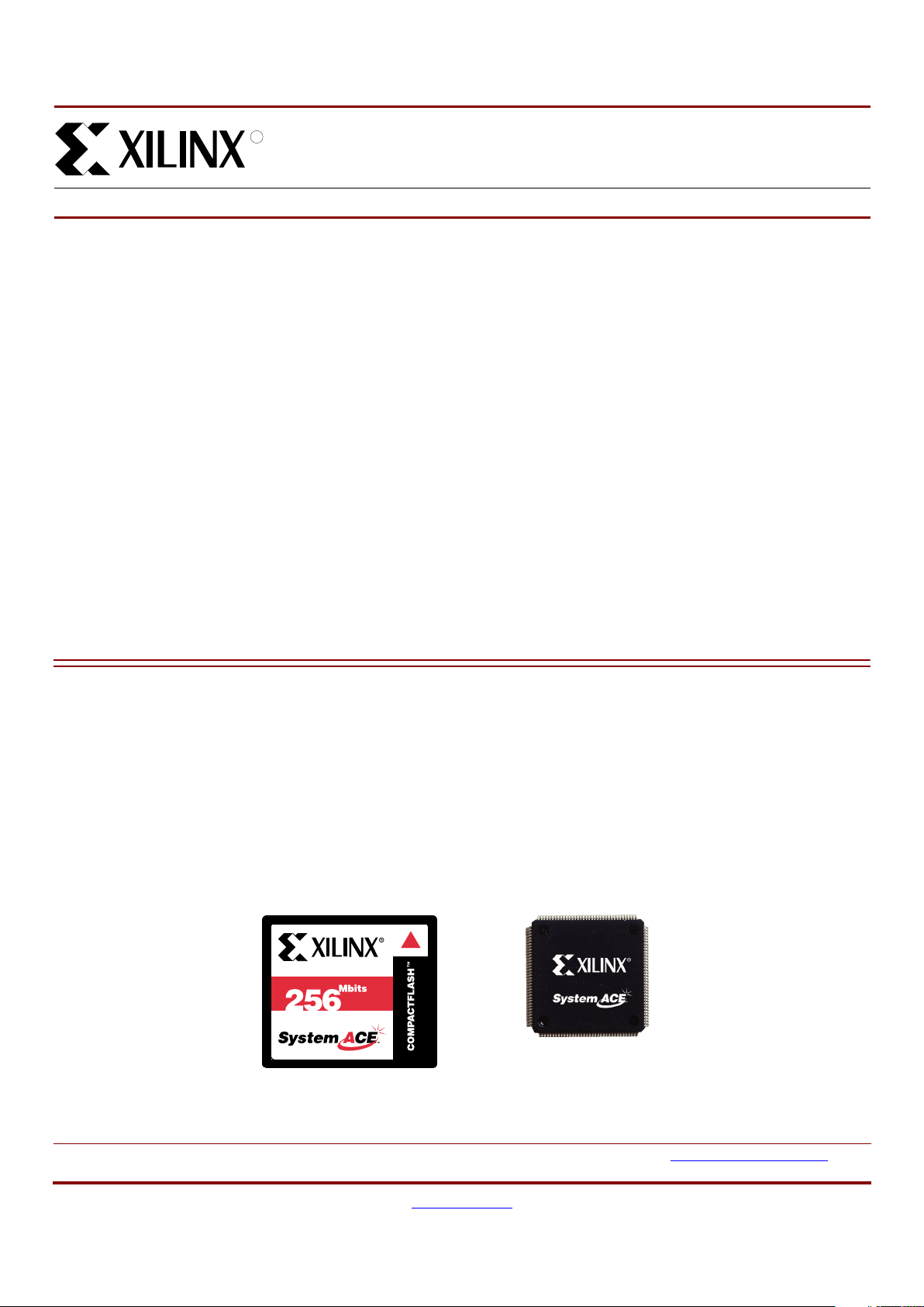
• ACE Flash (Xilinx-supplied Flash Cards):
- Densities of 128 Mbits and 256 Mbits
- CompactFlash Type I form factor
- PC Card ATA protocol compatible
- Noiseless and low CMOS power
- Automatic error correction and write retry capabilities
- Multiple partitions
- Program/erase over full commercial/industrial
temperature range
- Removable storage device
- Excellent quality and reliability
· MTBF >1,000,000 hours
· Minimum 10,000 insertions
• ACE Controller:
- CompactFlash interface supports ACE Flash
cards, standard third-party CompactFlash (Type I
or Type II) cards, and IBM Microdrives with up to
8 Gbit capacity
- Configuration of a target FPGA chain through
IEEE 1149.1 JTAG with a throughput up to
16.7 Mbits/sec
- Interfaces include CompactFlash, JTAG, and MPU
- MPU interface is compatible with microprocessor/
microcontroller bus interfaces, such as the IBM
PPC405, and Siemens 80C166
- IEEE 1149.1 Boundary-Scan Standard Compliant
(JTAG)
- FAT12/16 file system
- Compact 144-pin TQFP package
-Low power
General Description
Xilinx developed the System Advanced Con fig uration Environment (System ACE) family to address the need for a
space-efficient, pre- engineered, high-density configuratio n
solution for systems with multiple FPGAs. System ACE
technology is a ground-b reaking in-system programmable
configuration solution that provides substantial savings in
development effort and cost per bit over traditional PROM
and embedded solutions for high-capacity FPGA systems.
The System ACE family combines Xilinx expertise in configuration control with industry expertise in commodity memories. The first member of the System ACE family uses
CompactFlash.
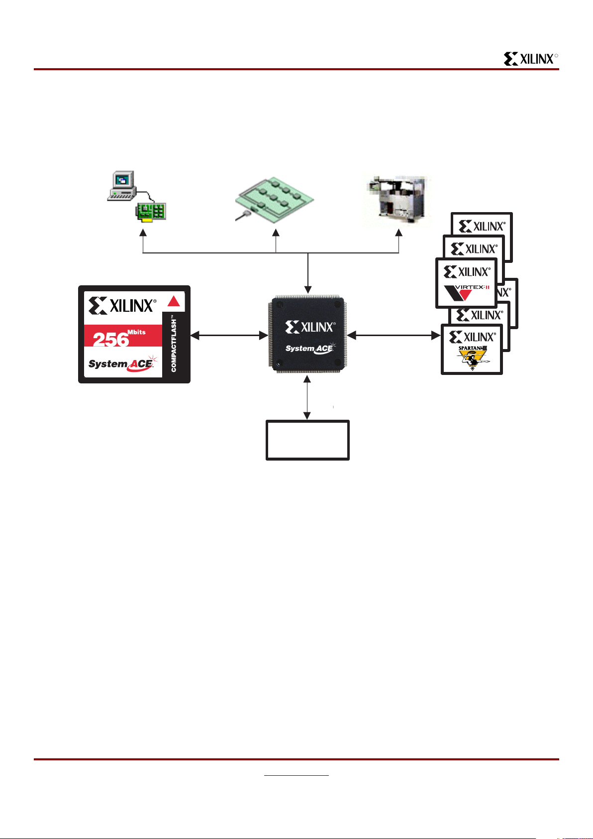
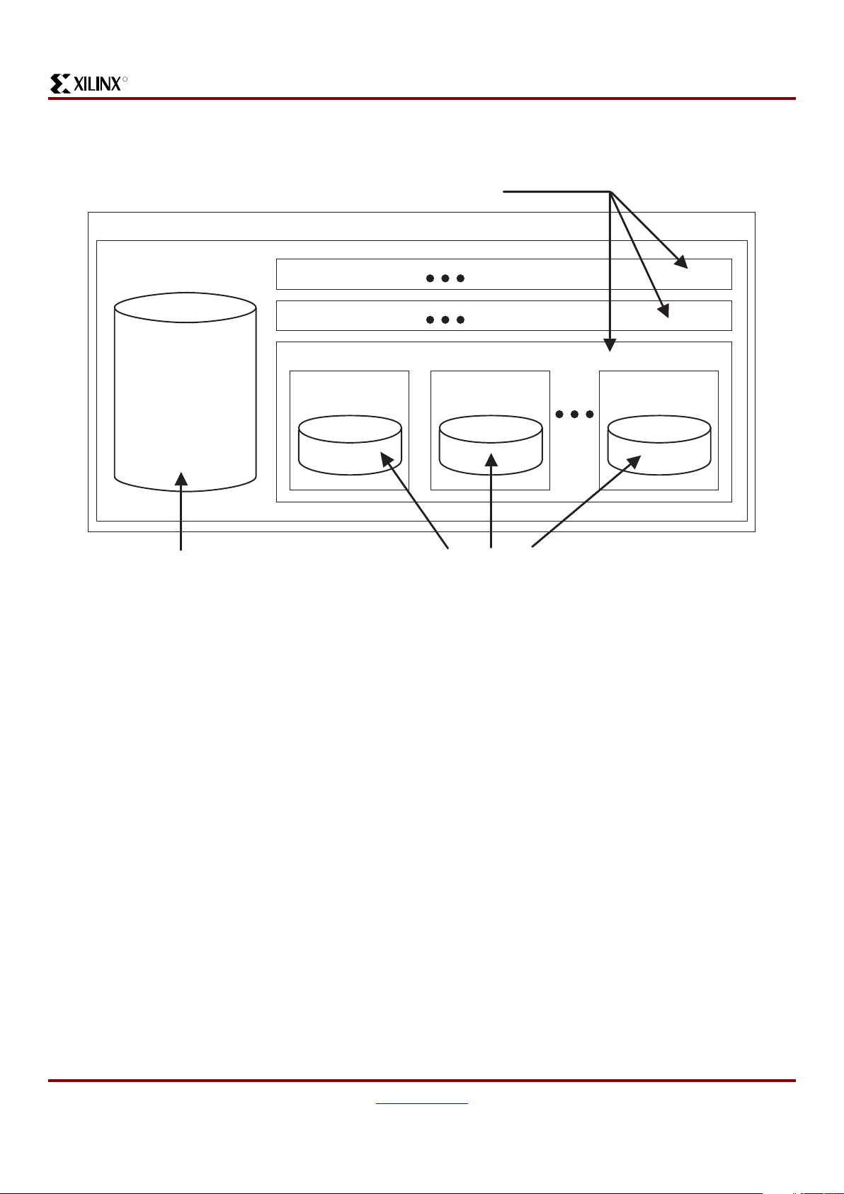
As shown in Figure 1, the System ACE CompactFlash solution is a chipset, consisting of a controller device (ACE Controller) and a CompactFlash storage device (ACE Flash).
0
System ACE
CompactFlash Solution
DS080 (v1.4) January 3, 2002
00
Advance Product Specification
R
Figure 1: System ACE Chipset
Interface to FPGA Target Chain
from CompactFlash, MPU,
or Test JTAG Port
ACE Flash
CompactFlash Storage Device
DS080_01_032101
128 Mbits or 256 Mbits
System ACE
Controller Device
Page 2
System ACE CompactFlash Solution
2 www.xilinx.com DS080 (v1.4) January 3, 2002
1-800-255-7778 Advan ce Product Specification
R
Figure 2 shows that the ACE Controller contains multiple
interfaces, including CompactFlash, MPU, and JTAG, to
allow for a highly flexible configuration solution . For added
flexibility , a CompactFlash or IBM Microdrive storage device
such as the Xilinx ACE Flash card can be used to store mul-
tiple bitstreams, with a capacity of up to 256 Mbits. The
combination of the ACE Controller and a standard CompactFlash or IBM Microdrive storage device delivers a powerful configuration solution for high-density FPGA systems.
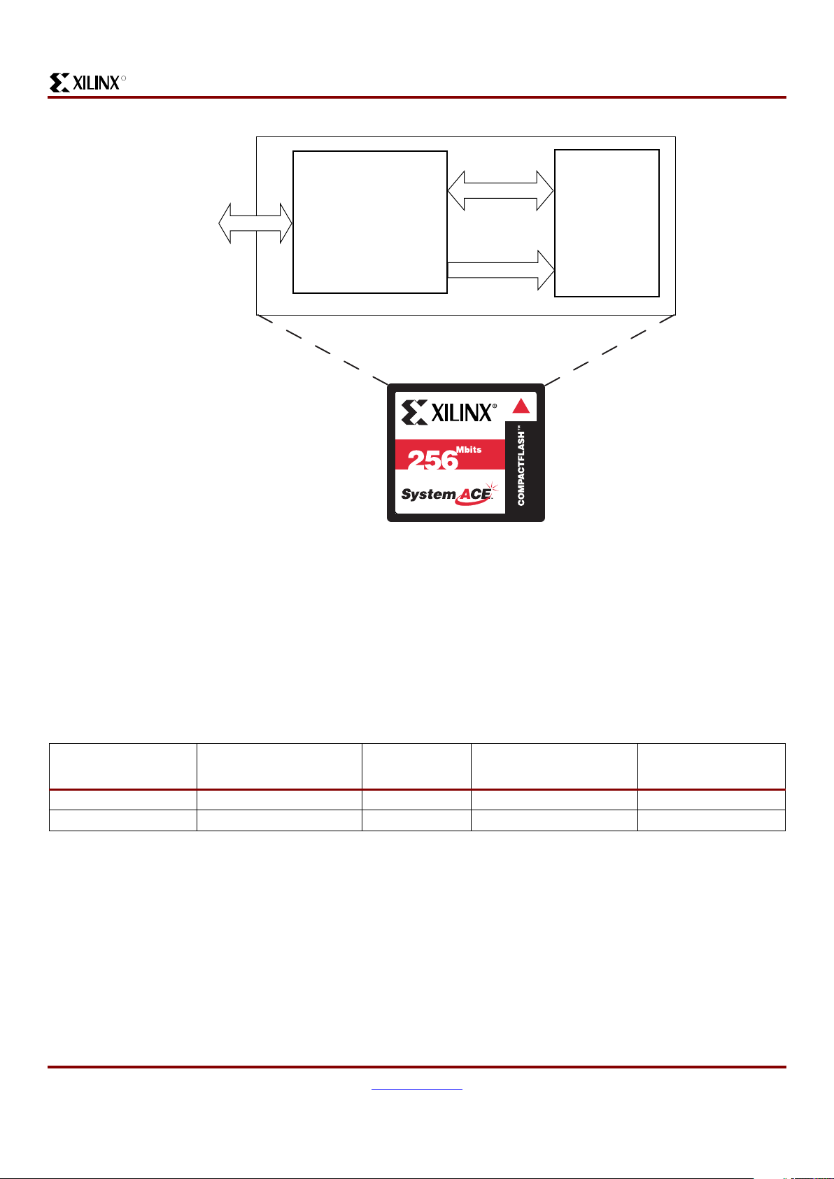
ACE Flash Memory Card
The Xilinx ACE Flash memory card is a CompactFlash
solid-state storage d evice that complies with the Personal
Computer Memory Card International Association ATA
(PCMCIA ATA) specifi cation. The ACE Flash card is available in two densities: 128 Mbits and 256 Mbits. This card
contains an on-card intelligent controller that manages
interface protocols, data storage a nd retr ieval, ECC, defect
handling and diagnostics, power management, and clock
control.
Using commerciall y available, low-cost peripheral devices,
the ACE Flash card can be programmed independently in a
PC environment, in which the Flash card appears as an
additional hard dri ve. Besides these standa rd options, the
System ACE solution allows for in-system programming of
an ACE Flash card through the ACE Controller MPU interface.
The ACE Flash card also interfaces dir ectly with the ACE
Controller to provide a powerful pre- engineered configuration solution. See Figure 3.
Figure 2: ACE Controller Interfaces
MPU Interface
Boundary-Scan Test Tools
PC-Based Tools
Embedded
MPU
Automatic Test Equipment
FPGA
Target Chain
DS080_02_032201
Configuration JTAG
Interface (CFGJTAG)
Test JTAG Interface
(TSTJTAG)
CompactFlash
Interface
ACE Flash,
Third Party CompactFlash,
or IBM Microdrive
Page 3
System ACE CompactFlash Solution
DS080 (v1.4) January 3, 2002 www.xilinx.com 3
Advance Product Specification 1-800-255-7778
R
System ACE File Structure
The System ACE file structure setup allows ACE Flash
memory not us ed for configuration storage to be used as
scratchpad memor y for other system storage needs. The
ability to store multip le bitstreams empowers designer s to
use a single ACE Flash card to run BIST patterns, PCI
applications, or store multiple bitstream variations of a
design (for example, versions for different geographical
regions).
The file structur e als o gives desig ner s the flexibility to st or e
supporting information with the bitstreams in addition to
configuration data, such as release notes, user guides,
FAQs, or other supporting files.
Figure 3: ACE Flash Card Block Diagram
DS080_03_032101
CompactFlash Internal
Single Chip Controller
Host
Interface
Data In/Out
CompactFlash
Modules
Control
Table 1: ACE Flash Card Capacity Specifications
Capacity (Bits)
Sectors/Card
(Max LBA+1)
Number of
Heads
Number of
Sectors/Tracks
Number of
Cylinders
128,450,560 31,360 2 32 490
256,901,120 62,720 4 32 490
Page 4
System ACE CompactFlash Solution
4 www.xilinx.com DS080 (v1.4) January 3, 2002
1-800-255-7778 Advan ce Product Specification
R
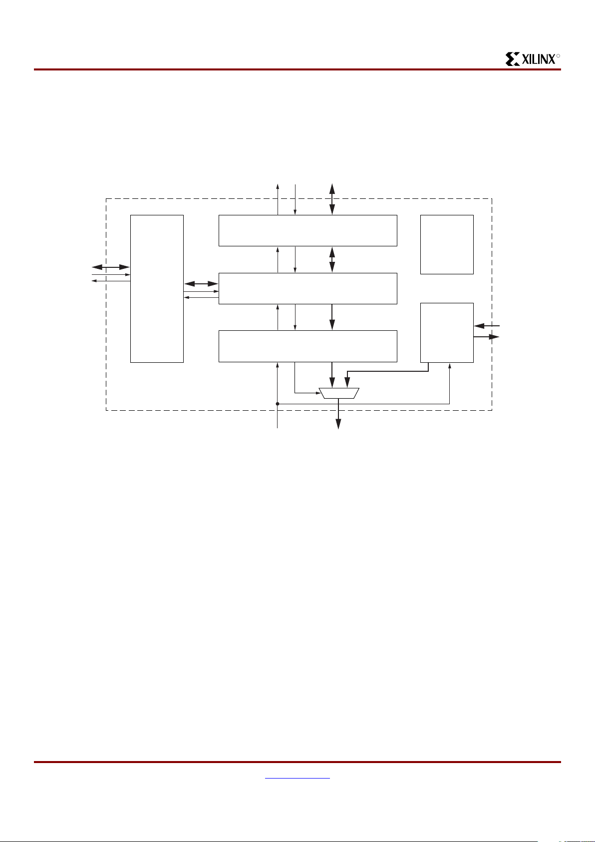
ACE Controller
The ACE Controller manages FPGA configuration data.
The controller provides an inte lligent interface between an
FPGA target chain and various supported configuration
sources; it can target multiple FPGA devices using JTAG at
a selectable throughput of up to 16.7 Mbits/sec. As shown in
Figure 4, three interfaces ar e availa b le for con fi g uri n g a ta r -
get FPGA chain through the Configuration JTAG Port.
These interfaces are: CompactFlash, Microprocessor
(MPU), and Test JTAG.
The directory structure used by the ACE Controller enables
it to support both CompactFlash and IBM Microdrive
devices through the CompactFlash port.
The MPU interface has acces s to the CompactFlash port,
the Configuration JTAG port, and local control/statu s features. The Test JTAG port is used when doing Boundary-Scan testing of the target FPGA chain or the ACE
Controller. Details about each interface are discussed
below.
The ACE Controller has two mai n power suppli es: the core
power supply (V
CCL
) and a CompactFlash /Test JTAG inter-
face power supply (V
CCH
). The V
CCH
power so urce suppl ies
the Test JTAG and CompactFlash port levels. These two
interfaces must be powered at 3.3 V. The V
CCL
core power
source supplies the MPU and Configuration JTAG ports,
which can be run at 3.3V or 2.5V. It is important to note that
these two interfaces are always powered at the same voltage. Considerations for the interface voltage are disc ussed
in Typical Configuration Modes, page 35. See Figure 5.
Figure 4: System ACE Controller Block Diagram
DS080_04_030801
CompactFlash Port
MPU Port
Test JTAG (TSTJTAG) Port
Configuration JTAG (CFGJTAG) Port
Configuration
JTAG Controller
CompactFlash
Arbiter
MPU
Control
and
Status
CompactFlash
Controller
Misc.
(LEDs,
etc.)
Test Scan
JTAG
Interface
(Target FPGA Chain)
Page 5

System ACE CompactFlash Solution
DS080 (v1.4) January 3, 2002 www.xilinx.com 5
Advance Product Specification 1-800-255-7778
R
Status Indicators
The ACE Controller has indicator pins to help monitor device status during operation.
Figure 5: ACE Controller I/O Requirements
DS080_05_030801
CompactFlash
CORE
CFGJTAG
MPU
TSTJTAG
LS LS LS LS
LS LS
Shaded output
buffers drive
V
OH
= V
CCL
=
2.5V or 3.3V
s
Shaded input
buffers sense
V
IH
= V
CCL
=
2.5V or 3.3V
s
All non-shaded
output buffers
drive V
OH
=
V
CCH
= 3.3V
s
All non-shaded
input buffers sense
V
IH
= V
CCH
= 3.3V
s
"LS" denotes
level-shifter
s
Core voltage level =
V
CCL
= 2.5V or 3.3V
s
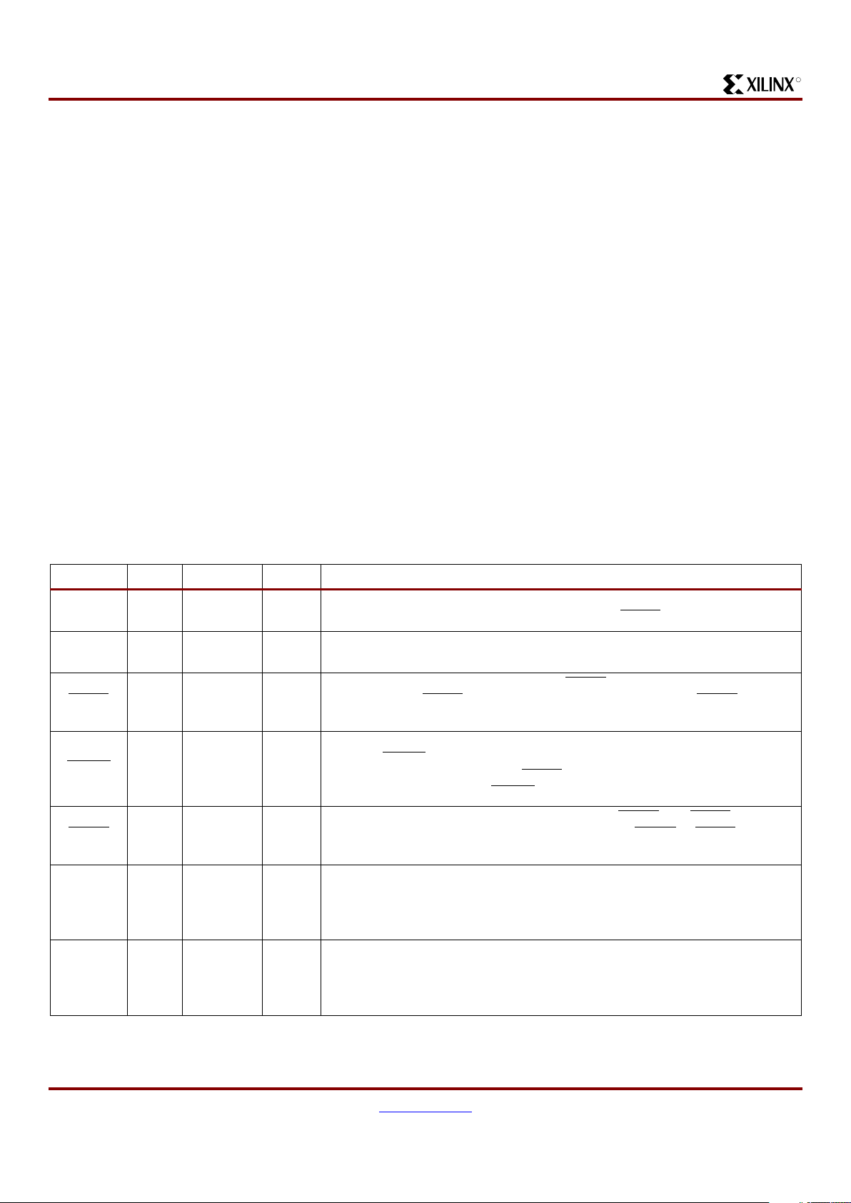
Table 2: ACE Controller Status Indicators
Name Pin Description
STATLED
95
• When on, the Status LED indicates that configuration is DONE.
• When blinking, this LED indicates that configuration is still in progress.
• When off this LED indicates that configuration is in an IDLE state.
ERRLED
96
• When on, the ERROR LED indicates that an error occurred.
• When blinking, this LED ind icates that no Co mpactFlash de vice w as f oun d when the Co mpactFlash
for the Configur ation JTAG interf ace w as enab led.
• When off, this LED indicates that no errors are detected.
Page 6
System ACE CompactFlash Solution
6 www.xilinx.com DS080 (v1.4) January 3, 2002
1-800-255-7778 Advan ce Product Specification
R
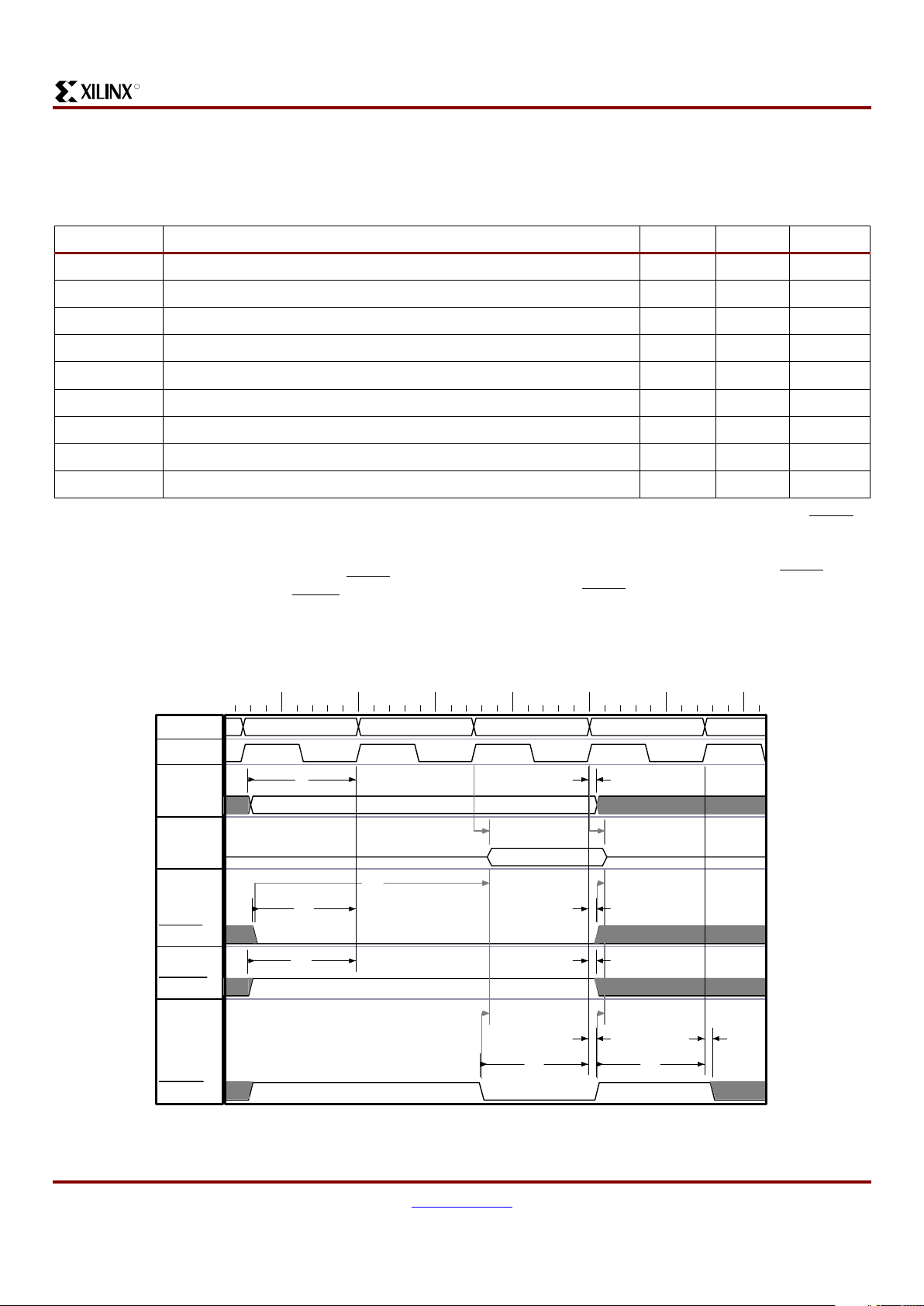
System ACE RESET
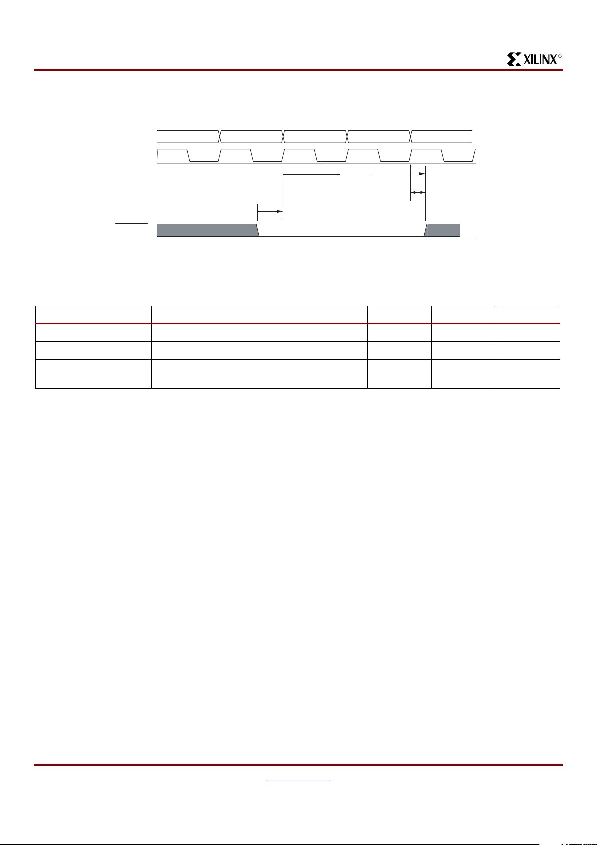
Notes:
1. When using the System ACE Controller RESET, TSRESET + TWRESET of three rising edges of CLK is required.
Figure 6: System ACE RESET Function Timing Diagram
CYCLE
CLK
RESET
Cycle 0
Cycle 1 Cycle 2 Cycle 3
TSRESET
THRESET
TWRESET
ds080_56_071801
Table 3: System ACE RESET
Symbol Parameter Min Max Units
TW(RESET) System ACE Controller Reset pulse width 3
(1)
rising edges
TH(RESET) Reset hold time after rising edge of CLK 0 ns
TS(RESET) System ACE Controller Reset setup up time
before rising edge of CLK
7
(1)
ns
Page 7
System ACE CompactFlash Solution
DS080 (v1.4) January 3, 2002 www.xilinx.com 7
Advance Product Specification 1-800-255-7778
R
Interfaces Overview
This section disc usses the details of each supported ACE
Controller interface.
CompactFlash Interface (CF)
The CompactFlash interface is the key ACE Controller interface for high-capacity systems. The CompactFlash port can
accommodate Xi linx ACE Flash c ards, any sta ndard CompactFlash module, or IBM Microdrives up to 8 Gbits, all with
the same form factor and board space requirements.
The use of standard Compac tFlash devices gives system
designers access to high-density Flash in a ver y efficient
footprint that does not change wi th density. CompactFlash
is a removable medium, which makes changes and/or
upgrades to the memory contents or density simple.
The CompactFlash interface is compr ised of two pieces: a
CompactFlash Controller, and a CompactFlash Arbiter. The
CompactFlash Contro ller detects the presence and maintains the status of the CompactFlash device. This Controller
also handles a ll CompactFlash device access bus cycles,
and abstracts and implements CompactFlash commands
such as soft res et, identify drive, and read/wr ite sector(s).
The CompactFlash Arbiter controls the in terface between
the MPU and the Configura tion JTAG Controller for access
to the CompactFlash data buffer.
CompactFlash devices are compliant with multiple read and
write modes. The System ACE Configuration Controller
supports ATA Common Memor y Read and Write func tions
specifically. Figure 7 and Figure 8 provide detailed timing
information on these functions.
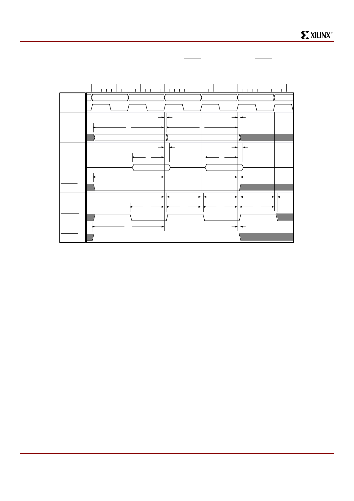
Figure 7: ACE Flash ATA Memory Write Timing Diagram
DS080_09_031301
ADDRESS
ADDRESS
REG
REG
DIN
DIN
CE
CE
WE
WE
WAIT
WAIT
TV(WT-WE)
(WT-WE)
DIN Valid
DIN Valid
TV(WT)
(WT)
T
SU
SU
(A)
(A)
T
SU
SU
(CE)
(CE)
TW(WE)
(WE)
TW(WT)
(WT)
T
SU
SU
(D - WEH)
(D - WEH)
TH(D)
(D)
TH(CE)
(CE)
T
REC
REC
(WE)
(WE)
Table 4: Common Memory Write Timing
Item Symbol IEEE Symbol Min (ns) Max (ns)
Data Setup before WE T
SU
(D-WEH) tDVWH 80
Data Hold following WE T
H
(D) tlWMDX 30
WE Pulse Width T
W
(WE) tWLWH 150
Address Setup Time T
SU
(A) tAVWL 30
CE Setup before WE T
SU
(CE) tELWL 0
Write Recovery Time T
REC
(WE) tWMAX 30
CE Hold following WE T
H
(CE) tGHEH 20
Wait Delay Falling from WE T
V
(WT-WE) tWLWTV 35
WE HIGH from Wait Release T
V
(WT) tWTHWH 0
Wait Width Time (Default Speed) T
W
(WT) tWTLWTH 350
Page 8
System ACE CompactFlash Solution
8 www.xilinx.com DS080 (v1.4) January 3, 2002
1-800-255-7778 Advance Product Specification
R
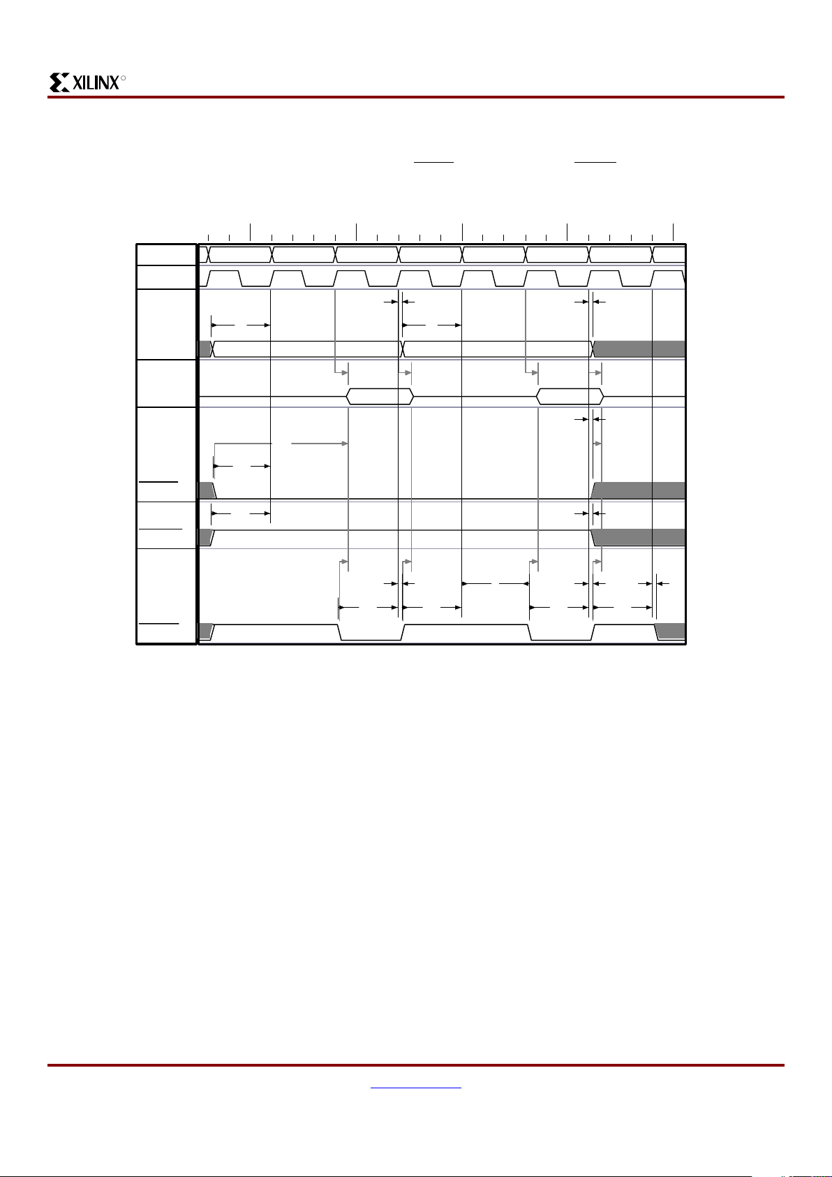
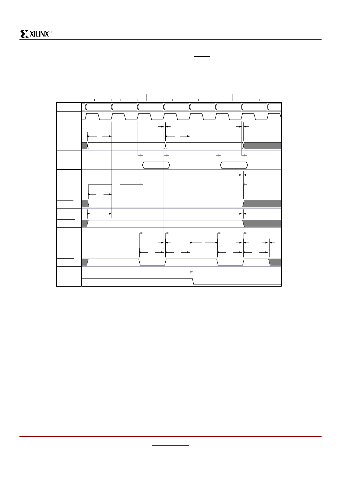
Figure 8: ACE Flash ATA Memory Read Timing Diagram
DS080_10_031301
ADDRESS
ADDRESS
REG
REG
DOUT
DOUT
CE
CE
OE
OE
WAIT
WAIT
TV(WT-OE)
(WT-OE)
TV(WT)
(WT)
T
SU
SU
(A)
(A)
T
SU
SU
(CE)
(CE)
TA(OE)
(OE)
TW(WT)
(WT)
TH(CE)
(CE)
TH(A)
(A)
T
DIS
DIS
(OE)
(OE)
Table 5: I/O Read Timing
Item Symbol IEEE Symbol Min (ns) Max (ns)
Data Delay after IORD T
D
(IORD) tlGLQV 100
Data Hold following IORD T
H
(IORD) tlGHQX 0
IORD Width Time T
W
(IORD) tlGLIGH 165
Address Setup before IORD T
SU
A(IORD) tAVIGL 70
Address Hold follow ing IORD T
H
A(IORD) tlGHAX 20
CE Setup before IORD T
SU
CE(IORD) tELIGL 5
CE Hold following IORD T
H
CE(IORD) tlGHEH 20
REG Setup before IORD T
SU
REG(IORD) tRGLIGL 5
REG Hold following IORD T
H
REG(IORD) tlGHRGH 0
INPACK Delay Falling from IORD T
DF
INPACK(IORD) tlGLIAL 0 45
INPACK Delay Rising from IORD T
DR
INPACK(IORD) tlGHIAH 45
IOIS16 Delay Falling from Address T
DF
IOIS16(ADR) tAVISL 35
IOIS16 Delay Rising from Address T
DR
IOIS16(ADR) tAVISH 35
Wait Delay Falling from IORD T
D
WT(IORD) tlGLWTL 35
Data Delay from Wait Rising T
D
(WT) tWTHQV 0
Wait Width Time (Default Speed) T
W
(WT) tWTLWTH 350
Page 9
System ACE CompactFlash Solution
DS080 (v1.4) January 3, 2002 www.xilinx.com 9
Advance Product Specification 1-800-255-7778
R
A basic understanding of the typical System ACE file and directory structure (shown in Figure 9) is useful when
programming an FPGA target system with a CompactFlash device in the System ACE solution.
The .ACE file is at the lowest level of the directory structure.
The Xilinx Syst em ACE software converts a revision of a
design (bitstream) into an .ACE file. An .ACE file re pr esen ts
a single set of bitstreams for a particular chain of devices.
The next level up in the file structure is a collection. The collection consists of eig ht .ACE files grouped together. All of
the .ACE files in a collection (directory) can be addresse d
when in the System ACE environment. There can be several collections stored on a CompactFla sh device, but only
one collection can be active at any given time.
The xilinx.sys file determines the collection from which
designs can be read.
The hierarchical design of the Sy stem ACE directo r y str ucture provides the ability to maintain multiple revisions or collections of different designs in a single ACE Flash device.
Each collect ion director y can contai n one or more des igns
that reside in different subdirecto ries. Each design subdirectory sh ould contain a singl e .ACE file that represents a
single set of bitstreams for a par ticular chain of devices. In
addition to FPGA configuration information, the collection
and design subdirectories can contain other information
pertain ing to the system design su ch as system software,
documentation, etc.
The xilinx.sys file in the root directory of the ACE Flash
device is used to control which of the designs within the
active collection is to be used to configu re the c hain of tar get devices. Only one collection, containing up to eight
designs, can be active at one time.
The ACE Controller parses the xilinx.sys file to determine
the active collection des igns and us es the thre e configuration address pins or MPU register bits (CFGADDR) to select
the desired design. If no xilinx.sys file exists in the root
directory of the ACE Flash device, a single .ACE file in the
root directory is used by System ACE as the active design.
Following are rules for the System ACE directory structure:
• System ACE configuration files must reside on the first
partition of the CompactFlash device.
• The System ACE partition must be formatted as FAT12
or FAT16.
• A xilinx.sys or single .ACE file must be in the root
(project) directory. An .ACE file is used only if the
xilinx.sys file cannot be found in this directory.
• Only one .ACE file should exist in the ROOT and/or
design directories. This directory structure allows the
Configuration controller to be able to use the .ACE file
to program the FPGA target system correctly.
Figure 9: System ACE Directory Structure
DS080_11_032101
dir = Rev_3;
cfgaddr0 = asia;
cfgaddr1 = europe;
cfgaddr3 = samerica;
cfgaddr4 = diag_1;
cfgaddr5 = diag_1;
cfgaddr6 = diag_2;
cfgaddr7 = diag_2;
xilinx.sys
Project Name - (root dir) "/"
*.ace *.ace *.ace
asia
(sub-dir)
europe
(sub-dir)
diag_2
(sub-dir)
Rev_3 (sub-dir)
Rev_2 (sub-dir)
Rev_1 (sub-dir)
CompactFlash
Available Collections
Collection Rev_3 Available Designs
for Target FPGA Chain
ACE System File
Containing Active Collection
(Up to 8 Designs)
Page 10
System ACE CompactFlash Solution
10 www.xilinx.com DS080 (v1.4) January 3, 2002
1-800-255-7778 Advance Product Specification
R
Microproce ssor Inte rf ac e (MPU)
The MPU Interface provides a useful me ans of monitorin g
the status of and controlling the Sy ste m ACE Contro ll er, as
well as ACE Flash card READ / WRITE data. T he MPU is
not required for normal operation, but when used, it provides numerous capabilities. This interface enables communication between an MPU device and a CompactFlash
module and the FPGA target system.
The MPU interface is composed of a set of registers that
provide a means for communicating with CompactFlash
control logic, configuration control logic, and other
resources in the ACE Contro ller. Specifically, this interface
can be used to read the identity of a Compac tFlash device
and read/write sectors from or to a CompactFlash device.
The MPU interface can also be used to control configuration
flow. The MPU interface enables monitoring of ACE Controller configuration status and error conditions. The MPU interface can be used to delay configuration, start configuration,
determine the source of configuration (CompactFlash or
MPU), control the bitstream version, reset the device, etc.
Two important issues should be understood when using the
microprocessor port:
• For the controller to be properly synchronized, the MPU
must provide the clock.
• The MPU must comply with System ACE timing diagrams.
This general-pur pose microproc essor interface can update
the CompactFlash, read the ACE status or obtain direct
access to the JTAG configuration ports using the ACE
Microprocessor commands. This interface suppor ts either
8-bit (default) or 16-bit data transfers. The bus width can be
configured dynamically.
All communications between the ACE Controller and a host
microprocessor involve transfer of data to or from ACE registers. There are 128 addres sable registers in 8- bit mode
and 64 addressable registers in 16-bit mode. For easy
selection of a new configuration from CompactFlash data,
the MPU interface allows for easy reconfiguration of an
FPGA chain or capability.
The following sections describe supported operations when
using the MPU interface.
MPU Port Signal Description
MPU interface port signals are described in Table 6.
Table 6: MPU Interface Port Signal Description
Name Width Direction Active Description
MPA 7 In N/A
Synchronous address inputs. The internal address register is loaded by MPA
by a combination of the rising edge of CLK and MPCE
LOW.
MPD 16 In/Out N/A
Synchronous data input/output pins. Both the data input and output path are
registered and triggered by the rising edge of CLK.
MPCE
1InLOW
Synchronous active LOW chip enable. MPCE
LOW is used to enable the
MPU interface. MPCE
LOW is also used in conjunction with MPOE LOW to
enable the MPD output.
MPWE
1InLOW
Synchronous active LOW write enable. A high-to-low-to-high transition must
occur on MPWE
in three consecutive clock cycles in order for the write to take
place.Du ring a va lid write cycle , MPCE
must be LOW a nd MPD must be valid
during the clock cycle that MPWE
.
MPOE 1InLOW
Asynchronous active LOW output enable. Both MPOE
and MPCE must be
LOW to read from the MPU interface. When either MPOE
or MPCE is HIGH,
the MPD pins of the ACE Controller are in a high-impedance state.
MPBRDY 1 Out HIGH
Synchronous active HIGH buffer ready output. During data buffer read mode
MPBRDY is HIGH when the data in the DATABUF buffer is valid. During data
buffer write mode MPBRDY is HIGH when data can be written to the
DATABUF buffer.
MPIRQ 1 Out HIGH
Synchronous active HIGH interrupt request output. MPIRQ HIGH indicates
that an interrupt condition has occurred in the MPU interface. All interrupt
conditions must be manually cleared before MPIRQ will go LOW. MPIRQ is
always LOW when interrupts are disabled.
Page 11
System ACE CompactFlash Solution
DS080 (v1.4) January 3, 2002 www.xilinx.com 11
Advance Product Specification 1-800-255-7778
R
MPU Timing Description
This section contai ns timing diagrams for the MPU interface. Parameters used in the timing dia grams are describ ed in
Table 7.
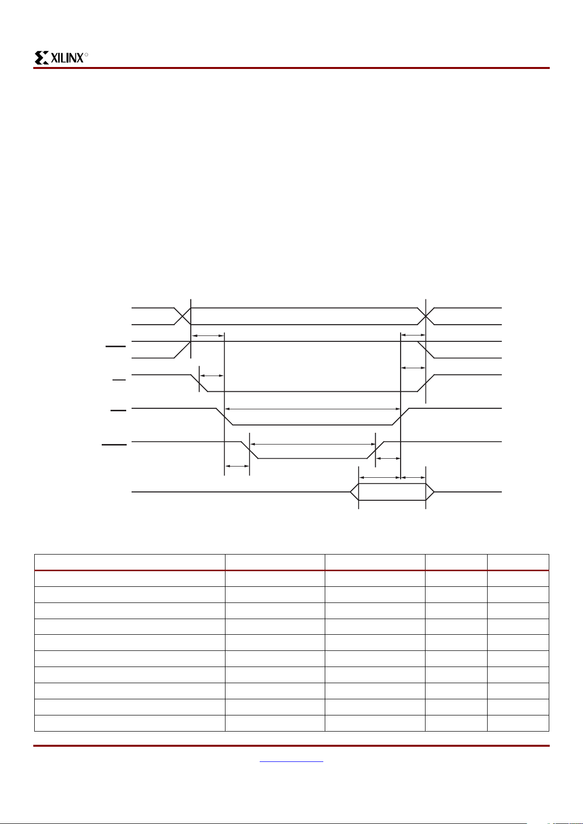
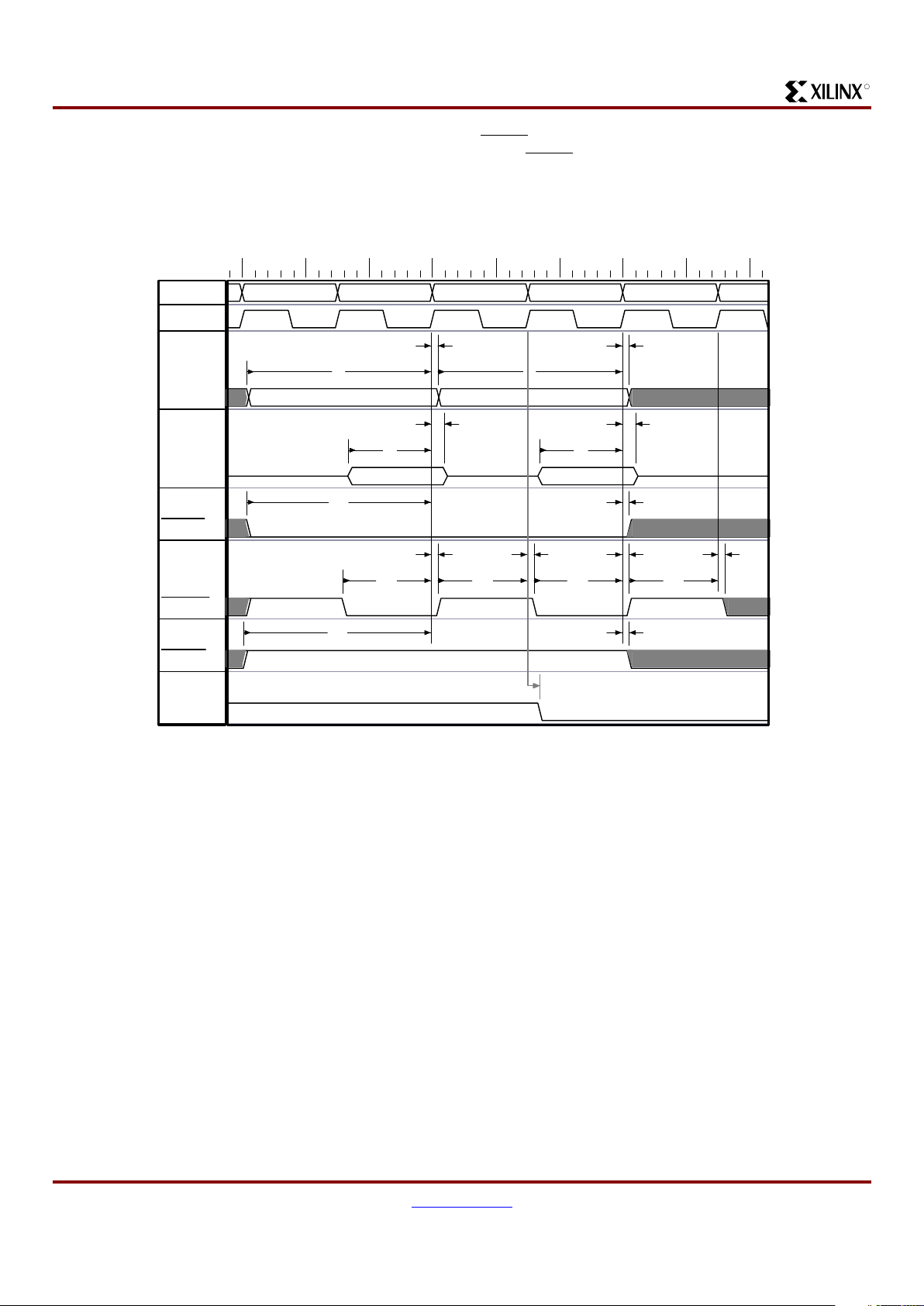
Single Register Read Cycle
The single regist er read cycl e is shown in Figure 10. A single register read is accomplished by asserting a valid
address (MPA), asser ting the chip enable (MPCE
= LOW)
and de-asser ting the write enable (MPW E
= HIGH) during
the first clock cycle (Cycle 0). These signals should hold
these values at least until the rising edge of the fourth clock
cycle (Cycle 3).
The output enable signal should be asserted (MPOE
=
LOW) during the th ird clock cycle ( Cycle 2). Regis ter data
associated with the spe ci fi ed a ddres s ap pears on the MP D
bus two clock cycles after the falling edge of MPCE
during
the assertion of MPCE
. The regist er read cycle i s then completed by de-asser ting the output enable dur ing the fourth
clock cycle (Cycle 3).
Table 7: MPU Interface Timing Parameters
Symbol Parameter Min Max Units
tSA Address setup time 4 -- ns
tSCE Chip enable setup time 4 -- ns
tSWE Write enable setup time 12 -- ns
tSOE Output enable setup time 12 -- ns
tSD Data setup time 4 -- ns
tDD Clock HIGH to valid data -- 22 ns
tDOE Chip/Output enable LOW to valid data -- 13 ns
tDBRDY Clock HIGH to buffer ready valid -- 22 ns
tH Hold time 0 -- ns
Figure 10: Single Read From an ACE Register
40ns 60ns 80ns 100ns 120ns 140ns 160
CYCLE
CLK
MPA
MPD
MPCE
MPWE
MPOE
Cycle 0 Cycle 1 Cycle 2 Cycle 3 Cycle 4
ADDRESS
DATA
tSA
tSCE
tSWE
tDD
tDOE tDOE
tDOE
tH
tH
tH
tDOE
tSOE
tH
tSOE
tH
tDD
DS080_14_013101
Page 12
System ACE CompactFlash Solution
12 www.xilinx.com DS080 (v1.4) January 3, 2002
1-800-255-7778 Advance Product Specification
R
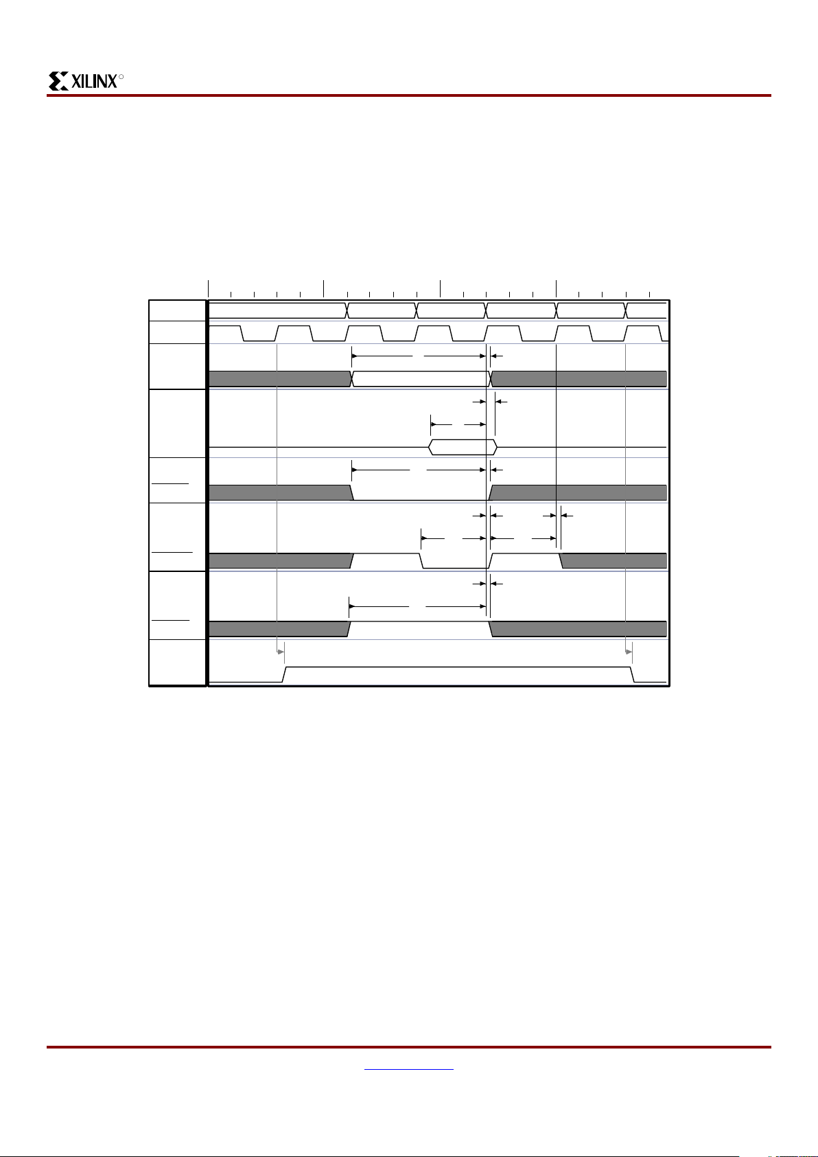
Single Register Write Cycle
The single regist er write cycle is sh own i n Figure 11. A single register write is accomplished by asserting a valid
address (MPA), asser ting the chip enable (MPCE
= LOW)
and de-asser tin g t he out put ena ble (MPOE
= HIGH) during
the first clock cycle (Cycle 0). These signals should hold
these values at least until the risin g edge of the thi rd clock
cycle (Cycle 2).
The write enable signal should be asserted (MPWE
= LOW)
during the second cl ock cycle (Cycle 1). Data (M PD) to be
written to the spec ified address should be asser ted d uring
the same clock cycle that the write enable is asserted
(Cycle 1). The register write cycle is then completed by
de-asserting the write enable during the third clock cycle
(Cycle 2).
Figure 11: Single WORD Write to an ACE Register
60ns 80ns 100ns 120ns 140ns 160
s
CYCLE
CLK
MPA
MPD
MPCE
MPWE
MPOE
Cycle 0 Cycle 1 Cycle 2 Cycle 3
ADDRESS
DATA
tSA
tSCE tH
tH
tH
tH
tSWE tSWE
tH
tSD
tH
tSOE
DS080_15_013101
Page 13
System ACE CompactFlash Solution
DS080 (v1.4) January 3, 2002 www.xilinx.com 13
Advance Product Specification 1-800-255-7778
R
Multiple Register Read Timing
The minimum timing requi rements for sequential r egister read c ycles are shown in Figure 12. Sequen tial read cycles are
identical to single read cycles, except that the chip enable (MPCE ) and write enable (MPW E) signals do not need to be
de-asserted between read cycles.
Figure 12: Multiple WORD Reads From ACE Register(s)
50ns 100ns 150ns 200ns 250
0
CYCLE
CLK
MPA
MPD
MPCE
MPWE
MPOE
Cycle 0 Cycle 1 Cycle 2 Cycle 3 Cycle 4 Cycle 5 Cycle 6 Cycle 7
ADDRESS <0> ADDRESS <1>
DATA <0> DATA <1>
tSA
tSCE
tSWE
tDD
tDOE tDOE
tH
tH
tDOE
tSOE
tH
tSOE
tH
tH
tSA
tDOE tDOE
tH
tSOE
tDOE
tH
tSOE
tDDtDD tDD
tH
DS080_16_013101
Page 14
System ACE CompactFlash Solution
14 www.xilinx.com DS080 (v1.4) January 3, 2002
1-800-255-7778 Advance Product Specification
R
Multiple Register Write Timing
The minimum timing requirements for sequential write
cycles are shown in Figure 13. Sequential write cy cles are
identical to single wri te cycles except that the chip enable
(MPCE
) and output enable (MPO E) signals do not need to
be de-asserted between write cycles.
Data Buffer Ready Timing
The data buffer ready (MPBRDY) signal indicates whether
the data buffer is ready to accept new data during a write
cycle or whether th e data buffer contains valid data to be
read during a read cycle. The data buffer itself is sixteen
words deep, where each word is 16 bits wide.
The data buffer mode transfer direction is id entified by the
state of the DATABUFMODE bit in the STATUSREG register:
• DATABUFMODE = 0 indicates data buffer read mode
• DATABUFMODE = 1 indicates data buffer write mode
The data buffer mode depends on the type of command that
was issued to the ACE Controller. If an IdentifyMemCard or
ReadMemCard command was issued, then the data buffer
remains in read mode until the command is finished executing (i.e., all sector data ha s been read from the buffer). If a
WriteMemCard c ommand was issu ed, then the data buffer
remains in write mode until the command is finished executing (i.e., all sector data has been written to the buffer).
Figure 13: Multiple WORD Writes to ACE Register(s)
60ns 80ns 100ns 120ns 140ns 160ns 180ns 200ns 22
CYCLE
CLK
MPA
MPD
MPCE
MPWE
MPOE
Cycle 0 Cycle 1 Cycle 2 Cycle 3 Cycle 4 Cycle 5
ADDRESS <0> ADDRESS <1>
DATA <0> DATA <1>
tSA
tSCE tH
tH
tH
tSWE tSWE
tH
tSD
tSOE
tSA
tH
tSD
tH
tH
tH tH
tSWE tSWE
tH
DS080_17_020101
Page 15
System ACE CompactFlash Solution
DS080 (v1.4) January 3, 2002 www.xilinx.com 15
Advance Product Specification 1-800-255-7778
R
Data Buffer Read Cycle Ready Timing
When the data buffer is in read mode and the last data word
is read from the buffer, the data buffer ready signal will go
inactive (MPBRDY = LOW) two clock cycles following the
last clock cycle that the output en able is active (MPOE
=
LOW). Any attempt to read data out of an “empty” data
buffer (MPOE
= LOW while MPBRDY = LOW) results in
invalid data. Valid and invalid data buffer reads are shown in
Figure 14.
Figure 14: Valid and Invalid Reads From DATABUFREG Data Buffer
50ns 100ns 150ns 200ns 250
CYCLE
CLK
MPA
MPD
MPCE
MPWE
MPOE
MPBRDY
Cycle 0 Cycle 1 Cycle 2 Cycle 3 Cycle 4 Cycle 5 Cycle 6 Cycle 7
DATABUFREG ADDRESS DATABUFREG ADDRESS
VALID DATA INVALID DATA
tSA
tSCE
tSWE
tDD
tDOE tDOE
tH
tH
tDOE
tSOE
tH
tSOE
tH
tH
tSA
tDOE tDOE
tH
tSOE
tDOE
tH
tSOE
tDDtDD tDD
tDBRDY
tH
DS080_18_020101
Page 16
System ACE CompactFlash Solution
16 www.xilinx.com DS080 (v1.4) January 3, 2002
1-800-255-7778 Advance Product Specification
R
Data Buffer Read Cycle Ready Timing
When the data buffer is in write mode and the last available
space for a data word has been filled, the data buffer ready
signal will go i nactive (MPBRDY = LOW) two clock cycles
following the last clock cycle that the wri te enable is active
(MPWE
= LOW). Any attempt to write da ta to a “full” data
buffer (MPWE
= LOW while MPBRDY = LOW) does not
result in a succes sful write to the buffer. Valid and invalid
data buffer writes are shown in Figure 15.
Figure 15: Valid and Invalid Writes to DATABUFREG Data Buffer
60ns 80ns 100ns 120ns 140ns 160ns 180ns 200ns 22
0
CYCLE
CLK
MPA
MPD
MPCE
MPWE
MPOE
MPBRDY
Cycle 0 Cycle 1 Cycle 2 Cycle 3 Cycle 4 Cycle 5
DATABUFREG ADDRESS DATABUFREG ADDRESS
VALID DATA INVALID DATA
tSA
tSCE tH
tH
tH
tSWE tSWE
tH
tSD
tSOE
tSA
tH
tSD
tH
tH
tH tH
tSWE tSWE
tH
tBRDY
DS080_19_020101
Page 17
System ACE CompactFlash Solution
DS080 (v1.4) January 3, 2002 www.xilinx.com 17
Advance Product Specification 1-800-255-7778
R
Interrupt Timing
The interrupt request and clearing cycles are shown in
Figure 16. In Figure 16, the interrupt request (MPIRQ =
HIGH) occurs sometime before Cycle 0. The interrupt
request is cleared by performing a single M PU write cycle
that sets RESETIRQ = 1 (bit number 11) in the CONTROLREG(15:0) register (BYTE address 0x19 or WORD address
0x0C).
The MPU interrupt request line (MPIRQ) remains active
HIGH until the RESETIRQ bit is set. The MPIRQ line
becomes inactive LOW two cycles after the comp letion of
the RESETIRQ wri te cy c le (Cyc l e 4 ). For subs equ ent MP U
interrupt requests to be enabled, the RESETIRQ bit must be
reset and one of the three IRQ enable bits (DATABUFRDYIRQ, ERRORIRQ, and/or CFGDONEIRQ) in the
CONTROLREG register should be set.
Figure 16: Interrupt Request Timing
0ns 50ns 100ns 150ns
CYCLE
CLK
MPA
MPD
MPCE
MPWE
MPOE
MPIRQ
Cycle 0 Cycle 1 Cycle 2 Cycle 3 Cycle 4
CONTROLREG(15:0) ADDRESS
0800h
tSA
tSCE tH
tH
tH
tH
tSWE tSWE
tH
tSD
tH
tSOE
tDIRQ tDIRQ
DS080_44_030501
Page 18
System ACE CompactFlash Solution
18 www.xilinx.com DS080 (v1.4) January 3, 2002
1-800-255-7778 Advance Product Specification
R
Register S p ec ification
The BYTE-mode register space of the MPU interface is shown in Table 8.
Table 8: Register Address Map (BYTE Mode Addresses)
BYTE Address
(MPA [6:0]) Register Name Width Mode Description
0x00 BUSMODEREG 1 RW Used to control the data bus access mode (8-bit
BYTE mode or 16-bit WORD mode)
0x01 BUSMODEREG 1 RW
0x02 -- -- -- Reser ved
0x03 -- -- -- Reser ved
0x04 STATUSREG(7:0) 8 R Used to monitor ACE Controller status
0x05 STATUSREG(15:8) 8 R
0x06 STATUSREG(23:16) 8 R
0x07 STATUSREG(31:24) 8 R
0x08 ERRORREG(7:0) 8 R Used to indicate any existing error condition
0x09 ERRORREG(15:8) 8 R
0x0A ERRORREG(23:16) 8 R
0x0B ERRORREG(31:24) 8 R
0x0C CFGLBAREG(7:0) 8 R Logical block address used by the Configuration
Controller during Compac tFlash data transfe rs
0x0D CFGLBAREG(15:8) 8 R
0x0E CFGLBAREG(23:16) 8 R
0x0F CFGLBAREG(27:24) 4 R
0x10 MPULBAREG(7:0) 8 RW Logical block address used by the MPU interface
during CompactFlash data transfers
0x11 MPULBAREG(15:8) 8 RW
0x12 MPULBAREG(23:16) 8 RW
0x13 MPULBAREG(27:24) 4 RW
0x14 SECCNTCMDREG(7:0) 8 RW Sector count and CompactFlash command
register
0x15 SECCNTCMDREG(15:8) 8 RW
0x16 VERSIONREG(7:0) 8 R Version register
0x17 VERSIONREG(15:8) 8 R
0x18 CONTROLREG(7:0) 8 RW Used to control ACE Controller operations
0x19 CONTROLREG(15:8) 8 RW
0x1A CONTROLREG(23:16) 8 RW
0x1B CONTROLREG(31:24) 8 RW
0x1C F ATST A TREG(7:0) 8 R Contains information about the FAT table of the first
valid partition found in the CompactFlash device.
0x1D FATSTATREG(15:8) 8 R
0x1E through 0x3F -- -- -- Reserved
Even V alues
0x40 through 0x7E
DAT ABUFREG(7:0) 8 RW Address range that provides read and write access
to the data buffer.
Odd Values
0x41 through 0x7F
DATABUFREG(15:8) 8 RW
Page 19
System ACE CompactFlash Solution
DS080 (v1.4) January 3, 2002 www.xilinx.com 19
Advance Product Specification 1-800-255-7778
R
The 16-bit WORD mode register space of the MPU interface is shown in Table 9.
Table 9: Register Address Map (WORD Mode Addresses)
WORD
Address
(MPA [6:1]) Register Name Width Mode Description
0x00 BUSMODEREG 1 RW Used to control the data bus access mode (8-bit BYTE
mode or 16-bit WORD mode)
0x01 -- -- -- Reserved
0x02 STATUSREG(15:0) 16 R Used to monitor ACE Contro ller status
0x03 STATUSREG(31:16) 16 R
0x04 ERRORREG(15:0) 16 R Used to indicate any existing error condition
0x05 ERRORREG(31:16) 16 R
0x06 CFGLBAREG(15:0) 16 R Logical block address used by the Configuration
Controller during CompactFlas h data transfers
0x07 CFGLBAREG(27:16) 12 R
0x08 MPULBAREG(15:0) 16 RW Logical block address used by the MPU interface during
CompactFlash data transfers
0x09 MPULBAREG(27:16) 12 RW
0x0A SECCNTCMDREG(15:0) 16 RW Sector count and CompactFlash command register
0x0B VERSIONREG(15:0) 16 R Version register
0x0C CONTROLREG(15:0) 16 RW Used to control ACE Controller operations
0x0D CONTROLREG(31:16) 16 RW
0x0E FATST ATREG(15:0) 16 R Contains information about the FAT table of the first valid
partition found in the CompactFlash device.
0x0F through
0x1F
-- -- -- Reserved
0x20 through
0x3F
DA TABUFREG(15:0) 16 RW Address range that provides read and write access to the
data buffer.
Page 20
System ACE CompactFlash Solution
20 www.xilinx.com DS080 (v1.4) January 3, 2002
1-800-255-7778 Advance Product Specification
R
BUSMODEREG Register (BYTE address 00h-01h, WORD address 00h)
The BUSMODEREG register is used to control the mode of the MPU address and data bus. The single-bit BUSMODEREG
register is aliased acros s two BYTE addresses (0x00-0x01) and one 16- bit WORD address (0x0). This register aliasing
ensures that the MPU bus mo de can be set re gardless of the mod e of the mi croproces sor that is communicati ng with th e
ACE Controller. Table 10 provides a description of the BUSMODEREG register bits.
STATUSREG Register (BYTE address 04h-07h, WORD address 02h-03h)
The STATUSREG register allows a microprocessor to monito r impor tant ACE Controller operati ng modes. This is also the
register that is rea d upon rece ivin g an IRQ req uest in o rder to id entify an inter r upt s ource. Table 11 provides a description
of the STATUSREG register bits.
Table 10: BUSMODEREG Register Bit Descriptions
Bit Name Description
0 BUSMODE0 The BUSMODE bits are used to select the width of the data bus portion of the
Microprocessor/Multi LINX bus (default is 0):
• When 0, the MPU interface is in BYTE mode (all MPU address bits are used, but only
MPU data bits 7:0 are used).
• When 1, the MPU interface is in WORD mode (all MPU data bits are used, but only
MPU address bits 6:1 are used).
1 -- Reserved
2 -- Reserved
3 -- Reserved
4 -- Reserved
5 -- Reserved
6 -- Reserved
7 -- Reserved
Table 11: STATUSREG Register Bit Descriptions
Bit Name Description
0 CFGLOCK Configuration controller lock status:
• 0 means that the configuration controller does not currently have a lock on the
CompactFlash controller resource
• 1 means that the configuration controller has successfully locked the CompactFlash
controller resource
1 MPULOCK MPU interface lock status:
• 0 means that the MPU interface does not currently have a lock on the CompactFlash
controller resource
• 1 means that the MPU interface has successfully locked the CompactFlash controller
resource
2 CFGERROR Configuration Controller error status:
• 0 means that no Configuration Controller error condition exists
• 1 means that an error has occurred in the Configuration Controller (check the
ERRORREG register for more information)
3 CFCERROR CompactFlash Controller error status:
• 0 means that no CompactFlash Controller error condition exists
• 1 means that an error has occurred in the CompactFlash controller (check the
ERRORREG register for more information)
Page 21
System ACE CompactFlash Solution
DS080 (v1.4) January 3, 2002 www.xilinx.com 21
Advance Product Specification 1-800-255-7778
R
4 CFDETECT CompactFlash detect flag:
• 0 means that no CompactFlash device is connected to the ACE Controller
• 1 means that a CompactFlash is connected to the ACE Controller
5 DATABUFRDY Data buffer ready status:
• 0 means that the data buffer is not ready for data transfer
• 1 means that the data buffer is ready for data to be transferred out of the buffer when
reading from the CompactFlash controller or into the buffer when writing to the
CompactFlash or Configuration controller
6 DATABUFMODE Data buffer mode status:
• 0 means read-only mode
• 1 means write-only mode
7 CFGDONE Configuration DONE status:
• 0 means that the configuration process has not completed
• 1 means that the entire ACE Controller configuration file has been executed and
configuration of all devices in the target Boundary-Scan chain is complete
8 RDYFORCFCMD Ready for CompactFlash controller command:
• 0 means not ready for command
• 1 means ready for command
9 CFGMODEPIN Configuration mode pin (note that this can be overridden by the CFGMODE bit in the
CONTROLREG register):
• 1 means automatically start the configuration process immediately after ACE
Controller Reset
• 0 means wait for CFGSTART bit in CONTROLREG before starting the configuration
process
10 -- Reserved
11 -- Reserved
12 -- Reserved
13 CFGADDRPIN0 Configuration address pins that are used as an offset into the system configuration file in
the CompactFlash device used to locate the ACE Controller configuration data file (note
that these pins can be overridden by the contents of the CFGADDRBIT[2:0] of the
CONTROLREG register)
14 CFGADDRPIN1
15 CFGADDRPIN2
16 -- Reserved
17 CFBSY CompactFlash BUSY bit (reflects the state of the BSY bit in the status register of the
CompactFlash device):
• 0 means that the CompactFlash device is not busy
• 1 means that the CompactFlash command register and data buffer cannot be
accessed; Bits 1-6 of the STATUSREG register are not valid when this bit is set
18 CFRD Y CompactFlash ready for operation bit (reflects the state of the RDY bit in the status register
of the CompactFlash device):
• 0 means the CompactFlash device is NOT ready to accept commands
• 1 means CompactFlash device is ready to accept commands
19 CFDWF CompactFlash data write fault bit (reflects the state of the DWF bit in the status register of
the CompactFlash device):
• 0 means that a write fault has NOT occurred
• 1 means that a write fault has occurred
Table 11: STATUSREG Register Bit Descriptions (Continued)
Bit Name Description
Page 22

System ACE CompactFlash Solution
22 www.xilinx.com DS080 (v1.4) January 3, 2002
1-800-255-7778 Advance Product Specification
R
ERRORREG Register (BYTE address 08h-0Bh, WORD address 04h-05h)
The ERRORREG register iden tifies specific information on any error conditions that might exist in the ACE Controller.
Table 12 provides a description of the ERRORREG register bits.
20 CFDSC CompactFlash ready bit (reflects the state of the DSC bit in the status register of the
CompactFlash device):
• 0 means that the CompactFlash device is NOT ready
• 1 means that the CompactFlash device is ready
21 CFDRQ CompactFlash data request bit (reflects the state of the DRQ bit in the status register of
the CompactFlash device):
• 0 means that no data is ready to be transferred to/from the data buffer of the
CompactFlash device
• 1 means that information be transferred to/from the data buffer of the CompactFlash
device
22 CFCORR CompactFlash correctable error bit (reflects the state of the CORR bit in the status register
of the CompactFlash device):
• 0 means that a correctable data error was NOT encountered
• 1 means that a correctable data error was encountered (check the ERRORREG
register for more information)
23 CFERR CompactFlash ERROR bit (reflects the state of the ERR bit in the status register of the
CompactFlash device):
• 0 means that no error has occurred during the execution of the previous command
• 1 means that the previous command has ended in some type of error (check the
ERRORREG register for more information)
24 -- Reserved
25 -- Reserved
26 -- Reserved
27 -- Reserved
28 -- Reserved
29 -- Reserved
30 -- Reserved
31 -- Reserved
Table 12: ERRORREG Register Bit Descriptions
Bit Name Description
0 CARDRESETERR CompactFlash card reset error:
• 0 means no error
• 1 means that the CompactFlash card has failed to reset properly before a time-out
condition occurred
1 CARDRDYERR CompactFlash card ready error:
• 0 means no error
• 1 means that the CompactFlash card has failed to become properly ready for
commands before a time-out condition occurred
2 CARDREADERR CompactFlash card read error:
• 0 means no error
• 1 means that a CompactFlash data read command (either ReadMemCardData or
IdentifyMemCard) has failed
Table 11: STATUSREG Register Bit Descriptions (Continued)
Bit Name Description
Page 23

System ACE CompactFlash Solution
DS080 (v1.4) January 3, 2002 www.xilinx.com 23
Advance Product Specification 1-800-255-7778
R
3 CARDWRITEERR CompactFlash card write error:
• 0 means no error
• 1 means that a CompactFlash data write command (WriteMemCardData) has failed
4 SECTORRDYERR CompactFlash sector ready:
• 0 means no error
• 1 means that a sector has failed to become properly valid during a CompactFlash read
or write command before a time-out condition occurred
5 CFGADDRERR CFGADDR error:
• 0 means no error
• 1 means that the CFGADDR (i.e., the CFGADDR(15:0) register or CFGADDR(1:0)
pins, depending on the state of the FORCECFGADDR bit in the CONTROLREG
register) does not correspond to a valid location in the CompactFlash
6 CFGFAILED Configuration failure error:
• 0 means no error
• 1 means that configuration of one or more devices in the target Boundary-Scan chain has
failed
7 CFGREADERR Configuration read error:
• 0 means no error
• 1 means that an error occurred while reading con fig urati on inform ation f rom
CompactFlash
8 CFGINSTRERR Configuration instruction error:
• 0 means no error
• 1 means that an invalid instruction was encountered during configuration
9 CFGINITERR Configuration INIT monitor error:
• 0 means no error
• 1 means that the CFGINIT
pin did not go HIGH within 500 ms of the start of
configuration
10 -- Reserved
11 CFBBK CompactFlash bad block error (reflects the state of the BBK bit in the error register of the
CompactFlash device):
• 0 means no error
• 1 means that a bad block has been detected
12 CFUNC CompactFlash uncorrectable error (reflects the state of the UNC bit in the error register of
the CompactFlash device):
• 0 means no error
• 1 means that an uncorrectable error has been encountered
13 CFIDNF CompactFlash ID not found error (reflects the state of the IDNF bit in the error register of
the CompactFlash device):
• 0 means no error
• 1 means that the requested sector ID is in error or cannot be found
14 CFABOR T CompactFlash command abort error (reflects the state of the ABRT bit in the error register
of the CompactFlash device):
• 0 means no error
• 1 means that the command has been aborted because of a CompactFlash status
condition (i.e., Not Ready, Write Fault) or when an invalid command has been issued
Table 12: ERRORREG Register Bit Descriptions (Continued)
Bit Name Description
Page 24

System ACE CompactFlash Solution
24 www.xilinx.com DS080 (v1.4) January 3, 2002
1-800-255-7778 Advance Product Specification
R
15 CFAMNF CompactFlash general error (reflects the state of the AMNF bit in the error register of the
CompactFlash device):
• 0 means no error
• 1 means that a general error has occurred
16 -- Reserved
17 -- Reserved
18 -- Reserved
19 -- Reserved
20 -- Reserved
21 -- Reserved
22 -- Reserved
23 -- Reserved
24 -- Reserved
25 -- Reserved
26 -- Reserved
27 -- Reserved
28 -- Reserved
29 -- Reserved
30 -- Reserved
31 -- Reserved
Table 12: ERRORREG Register Bit Descriptions (Continued)
Bit Name Description
Page 25

System ACE CompactFlash Solution
DS080 (v1.4) January 3, 2002 www.xilinx.com 25
Advance Product Specification 1-800-255-7778
R
CFGLBAREG Register (BYTE address 0Ch-0Fh, WORD address 06h-07h)
The CFGLBAREG read-o nly register contains the logical block address used by the ACE Contro ller configuration logic
during CompactFlash read/write opera tions. The CFGLBAREG regi ster affects only transfers between the ACE Controller
configuration logic and the CompactFlash card. The MPU uses a separate set of registers (MPULBAREG(27:0)) to transfer
data to and from the CompactFlash card. Table 13 provides a description of the CFGLBAREG register bits.
Table 13: CFGLBAREG Register Bit Descriptions
Bit Name Description
0 CFGLBA00 Logical Block Address used during CompactFlash read or write sector commands: each
block address points to a sector location which is made up of 512 bytes (i.e., maximum
CompactFlash device capacity is up to 128 gigabytes, or 137,438,953,472 bytes)
1CFGLBA01
2CFGLBA02
3CFGLBA03
4CFGLBA04
5CFGLBA05
6CFGLBA06
7CFGLBA07
8CFGLBA08
9CFGLBA09
10 CFGLBA10
11 CFGLBA11
12 CFGLBA12
13 CFGLBA13
14 CFGLBA14
15 CFGLBA15
16 CFGLBA16
17 CFGLBA17
18 CFGLBA18
19 CFGLBA19
20 CFGLBA20
21 CFGLBA21
22 CFGLBA22
23 CFGLBA23
24 CFGLBA24
25 CFGLBA25
26 CFGLBA26
27 CFGLBA27
28 -- Reserved
29 -- Reserved
30 -- Reserved
31 -- Reserved
Page 26

System ACE CompactFlash Solution
26 www.xilinx.com DS080 (v1.4) January 3, 2002
1-800-255-7778 Advance Product Specification
R
MPULBAREG Register (BYTE address 10h-13h, WORD address 08h-09h)
The MPULBAREG read-write register contains the logical block address that is used by the MPU interface during
CompactFlash read /wr ite op erati ons. The MP ULB A REG reg is ter af fects only tra ns fers between t he MPU in ter face and th e
CompactFlash card. ACE Contro ller configu ration logic ma intain s a separate set of r egisters ( CFGLBAR EG(27:0) ) for use
when transferring data to and from the CompactFlash card. Table 14 provides a description of MPULBAREG register bits.
Table 14: MPULBAREG Register Bit Descriptions
Bit Name Description
0 MPULBA00 Logical Block Address used during CompactFlash read or write sector commands: each
block address points to a sector location which is made up of 512 bytes (i.e., maximum
CompactFlash device capacity is up to 128 gigabytes, or 137,438,953,472 bytes)
1MPULBA01
2MPULBA02
3MPULBA03
4MPULBA04
5MPULBA05
6MPULBA06
7MPULBA07
8MPULBA08
9MPULBA09
10 MPULBA10
11 MPULBA11
12 MPULBA12
13 MPULBA13
14 MPULBA14
15 MPULBA15
16 MPULBA16
17 MPULBA17
18 MPULBA18
19 MPULBA19
20 MPULBA20
21 MPULBA21
22 MPULBA22
23 MPULBA23
24 MPULBA24
25 MPULBA25
26 MPULBA26
27 MPULBA27
28 -- Reserved
29 -- Reserved
30 -- Reserved
31 -- Reserved
Page 27

System ACE CompactFlash Solution
DS080 (v1.4) January 3, 2002 www.xilinx.com 27
Advance Product Specification 1-800-255-7778
R
SECCNTCMDREG Register (BYTE address 014h-15h, WORD address 0Ah)
The SECCNTCMDREG registe r provides the means for an
MPU interface to set the sector count and execute CompactFlash Controller commands. Table 15 provides a
description of the SECCNTCMDREG register bits.
The SECCNT bits of the SECCNTCMDREG register spec ify the number of sectors to transfer during each ReadMemCardData or WriteMemCardData command:
• A SECCNT value of 1 to 255 indicates to the
CompactFlash device that 1 to 255 sectors should be
transferred.
• A SECCNT value of 0 indicates that 256 sectors should
be transferred.
The CMD bits of the SECCNTCMDR EG register identify a
specific command to be executed:
• If the MPU has NOT successfully locked access to the
CompactFlash Controller, then writes to the CMD bits
of the SECCNTCMDREG register do not change the
value of the register.
• If the MPU has successfully locked access to the
CompactFlash Controller and a non-zero value is
written to the CMD bits of the SECCNTCMDREG
register, then the specified command is executed by
the CompactFlash Controller.
• If the MPU has successfully locked access to the
CompactFlash Controller and a zero value is written to
the CMD bits of the SECCNTCMDREG register, there is
no effect on the value of the CMD bits. The only way to
clear the CMD bits is to issue the cfAbort command,
which aborts the current ly execut in g co mman d an d
waits until the CompactFlash Controller clears the CMD
bits.
Table 15: SECCNTCMDREG Register Bit Descriptions
Bit Name Description
0 SECCNT0 Sector Count used during CompactFlash read or write sector commands: each sector is
made up of 512 bytes
1 SECCNT1
2 SECCNT2
3 SECCNT3
4 SECCNT4
5 SECCNT5
6 SECCNT6
7 SECCNT7
8 CMD0 Command value:
0x0 : Reserved
0x1 : ResetMemCard command
0x2 : IdentifyMemCard command
0x3 : ReadMemCardData command
0x4 : WriteMemCardData command
0x5: Reserved
0x6 : Abort command
0x7 : Reserved
9CMD1
10 CMD2
11 -- Reserved
12 -- Reserved
13 -- Reserved
14 -- Reserved
15 -- Reserved
Page 28

System ACE CompactFlash Solution
28 www.xilinx.com DS080 (v1.4) January 3, 2002
1-800-255-7778 Advance Product Specification
R
VERSIONREG Register (BYTE address 16h-17h, WORD address 0Bh)
The VERSIONREG register holds the ACE Controller version number in the form of a 4-bit major version field, a 4-bit minor
version field, and an 8-bit revision/build number field. Table 16 provides a description of the VERSIONREG register bits.
Table 16: VERSIONREG Register Bit Descriptions
Bit Name Description
0 VERSION0 Revision / build number: MSB is bit 7, LSB is bit 0
1 VERSION1
2 VERSION2
3 VERSION3
4 VERSION4
5 VERSION5
6 VERSION6
7 VERSION7
8 VERSION8 Minor version number: MSB is bit 11, LSB is bit 8
9 VERSION9
10 VERSION10
11 VERSION11
12 VERSION12 Major version number: MSB is bit 15, LSB is bit 12
13 VERSION13
14 VERSION14
15 VERSION15
Page 29

System ACE CompactFlash Solution
DS080 (v1.4) January 3, 2002 www.xilinx.com 29
Advance Product Specification 1-800-255-7778
R
CONTROLREG Register (BYTE address 18h-1Bh, WORD address 0Ch-0Dh)
The CONTROLREG register pr ovides the means for the MPU interface to control ACE Control ler functionality. Table 17
provides a description of the CONTROLREG register bits.
Table 17: CONTROLREG Register Bit Descriptions
Bit Name Description
0 FORC ELOCKREQ Forces the CompactFlash arbitration logic to grant a lock to t he MPU interface based on
the value of the LOCKREQ bit of the CONTROLREG register (default is 0):
• 0 means do not force MPU lock request (i.e., arbitrate between Configuration
Controller and MPU interface)
• 1 means force MPU lock request (i.e., do not perform arbitration: grant lock request
based only on MPU requests)
1 LOCKREQ CF arbitration lock request signal; Once a lock is granted, the LOCKREQ must be
de-asserted before the lock is removed (default is 0):
• 0 means do not request CompactFlash access lock
• 1 means request CompactFlash access lock
2 FORCECFGADDR Forces the ov erriding of the CFGADDR(1:0) pins in fav or of using the CFGADDRBIT(2:0)
bits of the CONTROLREG(15:13) register (default is 0):
• 0 means use the CFGADDR(1:0) pins
• 1 means use the CONTROLREG(15:13) register bits
3 FORCECFGMODE Forces the overriding of CFGMODEPIN in favor of using the CFGMODE bit of the
CONTROLREG register (defau lt is 0):
• 0 means use CFGMODEPIN
• 1 means use the CFGMODE bit of the CONTROLREG register
4 CFGMODE Configuration mode (default is 0):
• 1 means automatically start the configuration process immediately after ACE Controller
Reset
• 0 means wait for CFGSTART bit in CO NTR OLRE G bef or e starting the configur ation
process
5 CFGSTAR T Configuration start bit (default is 0):
• 0 means do not start configuration
• 1 means start configuration process
6 CFGSEL Configuration select (default is 0):
• 0 means configure from CompactFlash
• 1 means configure from MPU interface
7 CFGRESET Configuration/CompactFlash controller reset (default is 0):
• 0 means do not reset
• 1 means reset the Configuration and CompactFlash controllers (this also causes a
“soft-reset” of the CompactFlash device)
8 DATABUFRDYIRQ Data buffer ready IRQ enable (default is 0):
• 1 means interrupts are enabled for when data buffer is ready for transfer of data into or
out of the buffer
• 0 means data buffer ready interrupts are disabled
9 ERRORIRQ Error IRQ enable (default is 0):
• 1 means interrupts are enabled for when an error occurs
• 0 means error interrupts are disabled
Page 30

System ACE CompactFlash Solution
30 www.xilinx.com DS080 (v1.4) January 3, 2002
1-800-255-7778 Advance Product Specification
R
10 CFGDONEIRQ Configuration DONE IRQ enable (default is 0):
• 1 means interrupts are enabled for when configuration is DONE
• 0 means configuration DONE interrupts are disabled
11 RESETIRQ Resets the interrupt request line when a ’1’ is written to this register bit. Note that a ’0’ must
be written to this register bit in order to re-arm for subsequent interrupt conditions.
12
CFGPROG Inverted ACE Controller CFGPROG pin control (default is 0):
• 0 means set the
CFGPROG pin to its inactive HIGH state of 1
• 1 means set the
CFGPROG pin to its active LOW state of 0
13 CFGADDRBIT0 Configuration address register bits that are used as an offset into the system configuration
file in the CompactFlash device used to locate the ACE Controller configuration data file
(note that these register bits can be used to override the CFGADDR[2:0] pins of the ACE
Controller)
14 CFGADDRBIT1
15 CFGADDRBIT2
16 CFGRSVD0 Reserved for future use. These bits must be set to zero at all times.
17 CFGRSVD1
18 CFGRSVD2
19 -- Reserved
20 -- Reserved
21 -- Reserved
22 -- Reserved
23 -- Reserved
24 -- Reserved
25 -- Reserved
26 -- Reserved
27 -- Reserved
28 -- Reserved
29 -- Reserved
30 -- Reserved
31 -- Reserved
Table 17: CONTROLREG Register Bit Descriptions (Continued)
Bit Name Description
Page 31

System ACE CompactFlash Solution
DS080 (v1.4) January 3, 2002 www.xilinx.com 31
Advance Product Specification 1-800-255-7778
R
FATSTATREG Register (BYTE address 1Ch-1Dh, WORD address 0Eh)
The FATSTATREG register cont ain s infor m ati on abou t th e f ir st valid partition o f th e Co mpactFlash device such a s the boo t
record and FAT types found. Table 18 provides a description of the FATSTATREG register bits.
Table 18: FATSTATREG Register Bit Descriptions
Bit Name Description
0 MBRVALID Master boot record (MBR) valid flag:
• 0 means no MBR was detected
• 1 means a valid MBR was found
1 PBRVALID Partition boot record (PBR) valid flag:
• 0 means no PBR was detected
• 1 means a valid PBR was found
2 MBRFAT12 Master boot record (MBR) FAT12 flag:
• 0 means FAT12 flag is not set in MBR
• 1 means FAT12 flag is set in MBR
3 PBRFAT12 Partition boot record (PBR) FAT12 flag:
• 0 means FAT12 flag is not set in PBR
• 1 means FAT12 flag is set in PBR
4 MBRFAT16 Master boot record (MBR) FAT16 flag:
• 0 means FAT16 flag is not set in MBR
• 1 means FAT16 flag is set in MBR
5 PBRFAT16 Partition boot record (PBR) FAT16 flag:
• 0 means FAT16 flag is not set in PBR
• 1 means FAT16 flag is set in PBR
6 CALCFAT12 Calculated FAT12 flag (based on cluster count):
• 0 means not FAT12 (cluster count > 4085)
• 1 means FAT12 (cluster count < 4085)
7 CALCFAT16 Calculated FAT12 flag (based on cluster count):
• 0 means not FAT16 (cluster count > 65525)
• 1 means FAT16 (4085 < cluster count < 65535)
8 -- Reserved
9 -- Reserved
10 -- Reserved
11 -- Reserved
12 -- Reserved
13 -- Reserved
14 -- Reserved
15 -- Reserved
Page 32

System ACE CompactFlash Solution
32 www.xilinx.com DS080 (v1.4) January 3, 2002
1-800-255-7778 Advance Product Specification
R
DATABUFREG Register (BYTE address 40h-7Fh, WORD address 20h-3Fh)
The DATA BUFREG reg ister is the portal registe r to the data buffer that is used to transfer data between the MPU interface
and the CompactFlash and/or Configuration controllers. The descr iption of the DATABUFR EG register bits are shown in
Table 19.
Test JTAG Interface (TSTJTAG)
The Test JTAG Interface (TSTJTAG) supports 1149.1
Boundary-Scan operations on the ACE Controller and all
chained FPGA devices connected to the Configuration
JTAG (CFGJTAG) port. This interface can also be us ed to
program the target FPGA chain on the CFGJTAG port,
using Xilinx or third-party JTAG programming tools.
The ACE Controller is fully compliant with the IEEE 1149.1
Boundary-S can standard, commonly referred to as JTAG.
As shown in Figure 17, a T est Access P ort (TAP), instruction
decoder, and the required IEEE 1149.1 Registers are
included in the ACE Controller to suppor t the mandatory
Boundary-Sc an ins tructions. In addition, the Contro ll er als o
supports an optional 32-bit identification regis ter. Refer to
the 1149.1 Boundary-Scan standard specification for a
complete description of the required instructions and
detailed information on JTAG.
Table 19: DATABUFREG Register Bit Descriptions
Bit Name Description
0 DATA00 Data buffer portal register:
• Data register bits are read-only when the DATABUFMODE bit in the STATUSREG
register is a 0, otherwise they are write-only when the DATABUFMODE bit is a 1.
• DATABUFREG(07:00) are accessible in BYTE and WORD bus modes.
1DATA01
2DATA02
3DATA03
4DATA04
5DATA05
6DATA06
7DATA07
8 DATA08 Data register:
• Data register bits are read-only when the DATABUFMODE bit in the STATUSREG
register is a 0, otherwise they are write-only when the DATABUFMODE bit is a 1.
• DATABUFREG(15:08) are accessible in BYTE and WORD bus modes.
• During BYTE bus write mode, if the data buffer is ready, any writes to the
DATABUFREG(15:08) bits cause the DATABUFREG(15:00) contents to be written to
the data buffer.
• During BYTE bus read mode, if the data buffer is ready, the DATABUFREG(15:00)
register will hold the current value until the DATABUFREG(15:08) bits are read. After
DATABUFREG(15:08) is read, the DATABUFREG(15:00) register is loaded with any
pending new data.
9DATA09
10 DATA10
11 DATA11
12 DATA12
13 DATA13
14 DATA14
15 DATA15
Table 20: ACE Controller TAP Pins
Pins Description
TSTTDI (TDI) Test Data In
TSTTDO (TDO) Test Data Out
TSTTMS (TMS) Test Mode Select
TSTTCK (TCK) Test Clock
Page 33

System ACE CompactFlash Solution
DS080 (v1.4) January 3, 2002 www.xilinx.com 33
Advance Product Specification 1-800-255-7778
R
The TSTJT A G logic is connected to the CFGJTAG port as long as the CompactFlash and MPU interfaces are not connected
to the CFGJTAG port. Outlined in the following sections are the details of the JTAG interface for the ACE Controller.
The available Boundary-Scan registers for the ACE Controller are shown in Table 21.
Instruction Register
The Instruction Register (IR) for the ACE Controll er is eight bits wide and is co nnected between TDI and TDO dur ing an
instruction scan sequence. The Instruction Register is parallel loaded with a fixed instruction capture pattern in preparation
for an instruction sequence. This pattern is shifted out onto TDO (LSB first), while an instruction is shifted into the instruction
register from TDI. This pattern is illustrated in Table 22.
The optional IDCODE instruction is supported in addition to the mandatory instructions (BYPASS, SAMPLE/PRELOAD, and
EXTEST). The binary values for these instructions are listed in Table 23.
Figure 17: Test JTAG Interface Block Diagram
TAP
Controller
Logic
Identifcation Register
Instruction Register
Bypass Register
Boundary Scan Register
1
0
TSTTDI
TSTTMS
TSTTCK
CFGTDO
TSTTDO
CFGTCK
CFGTMS
CFGTDI
CFGSEL (from core)
CFGDATA (from core)
DS080_45_030801
Table 21: ACE Controller Boundary-Scan Registers
Register Name Register Length Description
Instruction Register 8 bits Holds current instruction OPCODE and captures internal device status.
Boundary-Scan Register 109 bits Controls and observes input, output, and output enable.
Identification Register 32 bits Captures device IDCODE.
Bypass Register 1 bit Device bypass.
Table 22: Instruction Register Values Loaded into IR During Instruction Scan Sequence
IR[7] IR[6] IR[5] IR[4] IR[3] IR[2]
IR[1:
0]
CFGINSTRERR
(MPU ERRORREG
register bit)
CFGFAILED
(MPU ERRORREG
register bit)
CFGREADERR
(MPU ERRORREG
register bit)
CFCERROR
(MPU STATUSREG
register bit)
CFGERROR
(MPU ST A TUSREG
register bit)
CFGDONE 01
Page 34

System ACE CompactFlash Solution
34 www.xilinx.com DS080 (v1.4) January 3, 2002
1-800-255-7778 Advance Product Specification
R
Boundary-Scan Register
The Boundary -Sc an regis te r, which is the primary test data register, is used to control and observe the state of device pins
during EXTEST and SAMP LE/PRELOAD instructi ons. For more information on the System ACE Boundar y-Scan register
(such as bit sequence, 3-state control, and so forth), refer to the System ACE Boundary-Scan Description Language (BSDL)
file available from the software download area at:
www.xilinx.com.
Bit Sequence
The bit sequence of the device is obtai nable from the B oundary-Scan Des cri ption Langu age (BSDL) Files. These files ar e
available from the software download area at:
www.xilinx.com.
Identification Register
The Identification Register known as the IDCODE is a fixed, vendor-assigned value that is used to electronically identify the
type of device and the manufacturer for a specific device being tested. The ACE Controller IDCODE register is 32 bits wide.
The contents of this register can be shifted out for examination by selecting the IDCODE instruction. The IDCODE is
available to any other system component vi a JTAG. The IDCODE register has the following binary format, described in
Table 24: vvvv:ffff:ffff:aaaa:aaaa:cccc:cccc:ccc1
Bypass Register
The last standard 1149.1 Boundary-Scan data register in the ACE Controller is the single flip-flop BYPASS register. It
directly passes data ser ially from the TDI pin to the TDO pin dur ing a bypass ins truct ion. This regi ster is init ialized to zero
when the TAP controller is in the UPDATE-DR state.
TAP Timing Characteristics
IEEE 1149.1 bounda ry-scan (JTAG) testing is per formed via the standar d 4-wire Te st Access Port (TAP). The Boundary
Scan timing waveforms and switching characteristics of the TAP are described in Figure 18 and Table 25, respectively.
Table 23: ACE Controller Boundary-Scan Instructions
Boundary-Scan Instruction Binary Code [7:0] Description
BYPA SS 11111111 Enables BYPASS
SAMPLE/PRELOAD 00000001 Enables boundary-scan SAMPLE/PRELOAD Operation
IDCODE 00001001 E nables sh ifting out 32- bi t IDCODE
EXTEST 00000000 Enables boundary-scan EXTEST operation
Table 24: ACE Controller Identification Register
Version Family Array Size Manufacturer Required by 1149.1
0000 0000001 00000000 00001001001 1
Figure 18: Test J TAG Boundary-Scan Port Timing Waveforms
0ns 50ns 100ns 150ns
2
TSTTMS
TSTTDI
TSTTCK
TSTTDO
VALID
TTCKTDO
TTAPTCK
TTAPTCK
TTCKTAP
TTCKTAP
DS080_46_030801
Page 35

System ACE CompactFlash Solution
DS080 (v1.4) January 3, 2002 www.xilinx.com 35
Advance Product Specification 1-800-255-7778
R
Configuration JTAG Interface (CFGJTAG)
Configuration JT A G P ort is the interface between the ACE Controller and the target FPGA chain. This port is accessed when
configuring the target FPGA chain of devices via any of the ACE Controller interfaces (Test JTAG, MPU, or CompactFlash).
To program o r test the FPGA targ et chain, the data from these interfaces is c onverted to 1149.1 B oundary-Scan (JTAG)
serial data.
Typical Configuration Modes
The four ACE Controller interfaces are designed to work together in a number of different combinations. This section
discusses typic al user co nfi gura tion mo des. A hand ful of s i gnal s determine wh ich i nter face provides the co nfi gurat ion dat a
source. Table 26 describes these important signals, and Table 27 shows how they work together to determine which
interface will be used. This is especially important when using multiple interfaces in a design, or when not using the default
values of these signals. The default values of these s ignals set th e CompactFla sh int erface as the source of configuratio n
data.
Table 25: System ACE Controller TAP Characteristics
Symbol Parameter Min Max Units
T
(TAPTCK)
TSTTMS and TSTTDI setup time before rising edge of TSTTCK 4 ns
T
(TCKTAP)
TSTTMS and TSTTDI hold times after TSTTCK 0 ns
T
(TCKTDO)
TSTTCK falling edges to TSTTDO output valid 16 ns
F
(TSTTCK)
Maximum TSTTCK clock frequency 16.7 MHz
Table 26: Configuration Signals Used for Selecting Configuration Modes and Active Design
Configuration Signal Description Default
CFGMODE Pin or MPU register bit CFGMODEPIN = 1
CFGMODE Register Bit = 0
CFGADDR[2:0] Pins or MPU register bits 0
CFGSEL MPU register bit 0
CFGSTART MPU re gister bit 0
CFGRESET MPU register bit (CFGRESET is a subset of the RESET
pin) 0
FORCECFGADDR MPU register bit (Overrides value on CFGADDR [2:0] pins) 0
FORCECFGMODE MPU register bit (Overrides value on CFGMODEPIN) 0
Table 27: Active Configuration Modes
Configuration Interface CFGMODE
(1)
CFGSEL CFGSTART CFGRESET
CompactFlash (Configure from CF immediately after reset) 10X
(2)
0
CompactFlash
(Configure from CF after receiving MPU start signal) 001 0
Microprocessor
(Configure from MPU after receiving MPU start signal) 111 0
Microprocessor
(Configure from MPU) 11X 0
Test JTAG
(Configure using the TSTJTAG port) 1X 0 0
Notes:
2. The FORCECFGMODE bit in the CONTROLREG register of the MPU interface can be used to force the CFGMODE register bit to
override the ACE Controller CFGMODEPIN.
3. An X entry indicates “don’t care”.
Page 36

System ACE CompactFlash Solution
36 www.xilinx.com DS080 (v1.4) January 3, 2002
1-800-255-7778 Advance Product Specification
R
CompactFlash (CF) to Configuration JTAG (CFGJTAG) Setup
This setup provides a standard CompactFlash interface for high-density FPGA systems. The CompactFlash interface is the
source of configuration data. The data configures the Xilinx FPGA chain through Boundary-Scan (JTAG) using the
Configuration JTAG port, as shown in Figure 19.
The ACE Controller handles all necessary steps to perform configuration from the CF to the target system. The appropriate
signal connections for this setup are shown in Figure 20. This setup can be used in conjunction with any of the other
interfaces.
Figure 19: Data Flow Diagram of CF to CFGJTAG
MPU
TSTTDI
TAP
CTRL.
CompactFlash
ACE
Controller
Core
TSTTDO
TDO
TDI
CFGTDO CFGTDI
TDI
TDO TDI TDOTDO TDI
DS080_22_030801
*CFCGTCK and CFGTMS lines are driven
by ACE Controller Core Logic and are broadcast
to all target devices.
BS NAC
(Test JTAG Port)
(Configuration JTAG Port)
Page 37

System ACE CompactFlash Solution
DS080 (v1.4) January 3, 2002 www.xilinx.com 37
Advance Product Specification 1-800-255-7778
R
CompactFlash (CF) to Microprocessor (MPU) Setup
This setup provides a standar d Compact Flash to MPU inter face for high-density FPGA sys tems. This inte rface provides a
great deal of flexibility. T he ability to communicate with the CF through the MPU port allows the user to perform many
operations, such as being able to switch the programming .ACE file so that it can be used for the target system.
Figure 20: Wiring Diagram for CF to CFGJTAG
ACE
Controller
CompactFlash
Device
CFD(15:0)
CFA(10:0)
D(15:0)
A(10:0)
Xilinx FPGA
Target Chain
CFGTMS TMS
CFGTCK
CFGTDI
CFGTDO
TCK
TDO
TDI
DS080_24_121201
CE1
CE2
WE
OE
WAIT
REG
CD1
CD2
CFCE1
CFCE2
CFWE
CFOE
CFWAIT
CFREG
CFCD1
CFCD2
CFGPROG
CFGINIT
PROGRAM
INIT
STATLED
RESET
ERRLED
V
CC
V
CC
5.1 kΩ
5.1 kΩ
1.0 kΩ
1.0 kΩ
RESET
V
CC
V
CC
180 Ω
180 Ω
5.1 kΩ
CFRSVD
V
CC
CFRESET
CSEL
IOWR
IORD
Figure 21: Data Flow Diagram of CF to MPU
TAP
CTRL.
TDO
TDI
CFGTDO CFGTDI
TDI
TDO TDI TDOTDO TDI
DS080_28_030801
BS NAC
MPU
CompactFlash
ACE
Controller
Core
TSTTDI
TSTTDO
(Test JTAG Port)
(Configuration JTAG Port)
Page 38

System ACE CompactFlash Solution
38 www.xilinx.com DS080 (v1.4) January 3, 2002
1-800-255-7778 Advance Product Specification
R
The ACE Controller handles all necessary steps to perform a CF to MPU operation. This setup uses the CF to MPU signals
shown in the wiring diagram in Figure 22.
Figure 22: Wiring Diagram CF to MPU
ACE Controller
MPU Device
CLK
MPBRDY
MPIRQ
MPA(6:0)
MPD(15:0)
DS080_27_121201
CompactFlash
Device
D(15:0)
A(10:0)
CFD(15:0)
CFA(10:0)
Refer to the microprocessor
or microcontroller data sheet
for appropriate signal names.
CE2
CE1
WE
OE
WAIT
REG
CD1
CD2
CFCE1
CFCE2
CFWE
CFOE
CFWAIT
CFREG
CFCD1
CFCD2
RESET
STATLED
ERRLED
MPCE
MPWE
MPOE
V
CC
V
CC
5.1 kΩ
5.1 kΩ
1.0 kΩ
1.0 kΩ
IOWR
IORD
CSEL
CFRESET
V
CC
V
CC
5.1 kΩ
CFRSVD
V
CC
180 Ω
180 Ω
Page 39

System ACE CompactFlash Solution
DS080 (v1.4) January 3, 2002 www.xilinx.com 39
Advance Product Specification 1-800-255-7778
R
Reading Sector Data from Compact Flash Control
Flow Process
Sector data can be read from the CompactFlash device via
the MPU interface of the SystemACE controller by following
the control flow sequence shown in Figure 23. The first step
in the sequence of accessing the CompactFlash interface is
to arbitrate for a lock. The control flow process for obtaining
a CompactFlash resource lock is shown in Figure 24. Once
the MPU interface has been granted a CompactFlash lock,
the MPU interface needs to make sure tha t the CompactFlash device is ready to receive a command. The process
for polling the command readiness indicator is shown in
Figure 25.
Figure 23: Reading Sector Data from CompactFlash Control Flow Process
Set ReadMemCardData
Command Control
Set MPU LBA
Set Sector
Count Control
Initialize Buffer
Count variable*
Read Data Buffer
Release CF Lock
Data is read.
Return success.
Buffer Count
equal to 0?
Decrement Buffer
Count variable
No
Yes
*Set Buffer Count variable equal to
the number of buffers in a sector transfer
= ((Sector Count)*(512 Bytes per sector))/
(32 bytes per buffer)
= (Sector Count) * (16 buffers per sector)
Read Data from CF
Get CF Lock
Check If Ready
For Command
• Write LBA bits 7:0 to byte address 10h
Write LBA bits 15:8 to byte address 11h
Write LBA bits 23:16 to byte address 12h
Write LBA bits 27:24 to byte address 13h
Write SECCNT bits 7:0 to byte address 14h
Write CFGRESET bit = 1 to byte address 18h
Write LOCKREQ
bit = 0 to byte
address 18h
Reset configuration
controller
Clear configuration
controller reset
Write CFGRESET
bit = 0 to byte
address 18h
Write CMD bits to byte address 15h
DS080_48_051701
Page 40

System ACE CompactFlash Solution
40 www.xilinx.com DS080 (v1.4) January 3, 2002
1-800-255-7778 Advance Product Specification
R
Once the CompactFlash device is ready to rec eive a new
command, the following informa tion needs to be wr itten to
the MPU interface:
1. The sector address or logical block address (LBA) of
the first sector to be transferred should be written to the
following MPU address locations:
- LBA[7:0] @ MPU byte address 10h
- LBA[15:8] @ MPU byte address 11h
- LBA[23:16] @ MPU byte address 12h
- LBA[27:24] @ MPU byte address 13h (note that
only four bits are used in the most significant LBA
byte)
2. The number of sectors to be read should be written to
the low byte of the SECCNTCMDREG register (MPU
byte address 14h)
3. The ReadMemCardData command (03h) should be
written to the high byte of the SECCNTCMDREG
register (MPU byte address 15h)
4. Reset the CFGJTAG controller by setting the
CFGRESET bit (bit 7) of the CONTROLREG register
(MPU address 18h) to a 1.
Immediately after wr iting the command to the MPU i nterface, the CFGJTAG controller should be reset before reading the sector data from the data buffer.
The control flow process for reading the sector data from
the data buffer is shown in Figure 26.
After all of the requested se ctor data has been read, the
CFGJTAG controll er should be taken out of reset an d the
CompactFlash lock should be released by setting the
LOCKREQ bit (bit 1) an d CFGRESET bit (bi t 7) of the low
byte of the CONTROLREG register (MPU byte address
18h) to a 0. Note that all requeste d sector data should be
read from the data buffer in order to avoid a deadlock situation with the CompactFlash device.
Page 41

System ACE CompactFlash Solution
DS080 (v1.4) January 3, 2002 www.xilinx.com 41
Advance Product Specification 1-800-255-7778
R
Get CompactFlash Lock Control Flow Process
The CompactFlash resource must be arbitrated for before it
can be accessed via t he MPU int erf a ce . Th e Comp act Flash
arbitration process is s hown in Figure 24. A CompactFlash
lock is requested by setting the LOCKREQ bit (bit 1) to a 1
in the CONTROLREG register (MPU address 18h) and polling the MPULOCK b it (bit 1) in the STATUSREG register
(MPU byte address 04h).
Note that if the CFGLOCK bit (bit 0) in the STATUSREG register (MPU byte address 04h) is set, then the CFGJTAG
controller has locked the CompactFlash resource. In this
case, the MPU interface must either wait for the CFGJTAG
interface to release the lock or it can force the lock to be
released. This is done by resetting th e CFGJ TAG controller
by setting the CFGRESET bit (bit 7) and the FORCELOCKREQ bit (bit 0) in the CONTROLREG register (M PU byte
address 18h). The lock request process can be started
again after forcing the CFGJTAG controller to release the
lock.
Figure 24: Get CompactFlash Lock Control Flow Process
CF Locked?
Timer Expired?
Decrement timer
variable
CF is busy.
Return timeout
error.
CF is locked.
Return success.
No
Yes
No
Yes
Write LOCKREQ bit = 1
to byte address 18h
Get CF Lock
Set Lock Control
Initialize timer variable
Get Lock Status
Read MPULOCK bit
from byte address 04h
DS080_49_051701
Page 42

System ACE CompactFlash Solution
42 www.xilinx.com DS080 (v1.4) January 3, 2002
1-800-255-7778 Advance Product Specification
R
Check if Ready fo r a Command Control
Flow Process
Before reading or writing sector data, it is important to make
sure that the CompactFlash device is ready for a command.
This is done by polling the RDYFORCFCMD bit (bit 0) in the
second byte of the STATUSREG register (MPU byte
address 05h) until it is set to a 1. This control flow process is
shown in Figure 25.
Figure 25: Check if Ready for a Command Control Flow Process
Check If Ready
For Command
Get Command
Ready Status
Ready For
Command?
Timer Expired?
Decrement timer
variable
Initialize timer variable
Busy.
Return timeout
error.
Ready.
Return success.
No
Yes
No
Yes
Read RDYFORCMD bit
from byte address 05h
DS080_50_051701
Page 43

System ACE CompactFlash Solution
DS080 (v1.4) January 3, 2002 www.xilinx.com 43
Advance Product Specification 1-800-255-7778
R
Read Data Buffer Control Flow Process
The control flow process for reading from the data buffer is
shown in Figure 26. The SystemACE data buffer is implemented as a 32-byte (16 -word) deep FIFO that is al iased
across a range of MPU byte addresses (40h through 7Fh) in
order to facilitate burst transfers across the MPU interface.
Sector data is read f rom the data buffer by first waiting for
the buffer to become ready (i.e., full of sector data), as
shown in Figure 27. Once the buffer is ready, then all 32
bytes can be read from the buffer from alternating even and
odd byte addresses. Reading from an odd byte address
while in BYTE mode causes the FIFO to increment the data
word to the next available word in the FIFO. Reading from
any data buffer address while in WORD mode will cause the
FIFO to increment.
Figure 26: Read Data Buffer Control Flow Process
Read data word
from buffer
Decrement Data
Count variable
Data Count
equal to 0?
Buffer is written.
Return success.
Yes
No
Wait for Buffer Ready
Read Data Buffer
Initialize Data
Count variable*
*Set Data Count variable equal to
the number of data items in a buffer
(e.g., 16 bytes or 32 words)
Read data bits 7:0 from byte address 40h
Read data bits 15:8 from byte address 41h
(Note that the following conditions must
be valid for a data read to occur from the
CompactFlash data buffer:
1. The data buffer must be ready
2. A single read from byte address 41h
must occur that will cause the entire 16bit data register to be overwritten by the
buffer with new data)
DS080_51_051701
Page 44

System ACE CompactFlash Solution
44 www.xilinx.com DS080 (v1.4) January 3, 2002
1-800-255-7778 Advance Product Specification
R
Wait for Buffer Ready Control Flow Process
The readiness of the Sys temACE data buffer indicates that
the buffer is either full during a ReadM emCardData command execution or empty during a WriteMemCardData
command execution. The control flow process for waiting for
the buffer to become ready is shown in Figure 27. The
buffer ready status can be obtained from either the
DATABUFR DY bit (bit 5) of the STATUSREG register (MPU
byte address 04h) or from the MPBRDY pin of the SystemACE controller.
Figure 27: Wait for Buffer Ready Control Flow Process
Wait for Buffer Ready
Get Buffer
Ready Status
Buffer Ready?
Timer Expired?
Decrement timer
variable
Initialize timer variable
Buffer not
ready. Return
timeout error.
Buffer is ready.
Return success.
No
Yes
No
Yes
Read DATABUFRDY bit
from byte address 04h
DS080_52_051701
Page 45

System ACE CompactFlash Solution
DS080 (v1.4) January 3, 2002 www.xilinx.com 45
Advance Product Specification 1-800-255-7778
R
Microprocessor (MPU) to CompactFlash (CF) Setup
This setup provides a communication path from the MPU to the CF device. The CompactFlash is the source of the
configuration data, and this path enables users to read the contents of the CF device.
The ACE Controller handles all nec essary steps to p erform an M PU to CF ope ration. Th e neces sar y signals for this setup
are shown in Figure 22.
Figure 28: Data Flow Diagram of MPU to CF
MPU
TSTTDI
TAP
CTRL.
CompactFlash
TSTTDO
TDO
TDI
CFGTDO CFGTDI
TDI
TDO TDI TDOTDO TDI
DS080_25_030801
BS NAC
ACE
Controller
Core
(Test JTAG Port)
(Configuration JTAG Port)
Page 46

System ACE CompactFlash Solution
46 www.xilinx.com DS080 (v1.4) January 3, 2002
1-800-255-7778 Advance Product Specification
R
Writing Sector Data to Compact Flash Control
Flow Process
Sector data can be wr itten to the Com pactFla sh device via
the MPU interface of the SystemACE controller by following
the control flow sequence shown in Figure 29. The first step
in the sequence of accessing the CompactFlash interface is
to arbitrate for a lock. The control flow process for obtaining
a CompactFlash resource lock is shown in Figure 24. Once
the MPU interface has been granted a CompactFlash lock,
the MPU interface needs to make sure tha t the CompactFlash device is ready to receive a command. The process
for polling the command readiness indicator is shown in
Figure 25.
Figure 29: Write Data to CompactFlash Control Flow Process
Set MPU LBA
Set WriteMemCardData
Command Control
Set Sector
Count Control
Initialize Buffer
Count variable*
Write Data Buffer
Release CF Lock
Data is written.
Return success.
Buffer Count
equal to 0?
Decrement Buffer
Count variable
No
Yes
*Set Buffer Count variable equal to
the number of buffers in a sector transfer
= ((Sector Count)*(512 Bytes per sector))/
(32 bytes per buffer)
= (Sector Count) * (16 buffers per sector)
Write Data to CF
Get CF Lock
Check If Ready
For Command
Write LBA bits 7:0 to byte address 10h
Write LBA bits 15:8 to byte address 11h
Write LBA bits 23:16 to byte address 12h
Write LBA bits 27:24 to byte address 13h
Write SECCNT bits 7:0 to byte address 14h
Write CFGRESET bit = 1 to byte address 18h
Write LOCKREQ
bit = 0 to byte
address 18h
Reset configuration
controller
Clear configuration
controller reset
Write CFGRESET
bit = 0 to byte
address 18h
Write CMD bits to byte address 15h
DS080_053_051701
Page 47

System ACE CompactFlash Solution
DS080 (v1.4) January 3, 2002 www.xilinx.com 47
Advance Product Specification 1-800-255-7778
R
Once the CompactFlash device is ready to rec eive a new
command, the following informa tion needs to be wr itten to
the MPU interface:
1. The sector address or logical block address (LBA) of
the first sector to be transferred should be written to the
following MPU address locations:
- LBA[7:0] @ MPU byte address 10h
- LBA[15:8] @ MPU byte address 11h
- LBA[23:16] @ MPU byte address 12h
- LBA[27:24] @ MPU byte address 13h (note that
only four bits are used in the most significant LBA
byte)
2. The number of sectors that will be written should be
loaded into the low byte of the SECCNTCMDREG
register (MPU byte address 14h)
3. The WriteMemCardData command (04h) should be
written to the high byte of the SECCNTCMDREG
register (MPU byte address 15h)
4. Reset the CFGJTAG controller by setting the
CFGRESET bit (bit 7) of the CONTROLREG register
(MPU address 18h) to a 1.
Immediately after wr iting the command to the MPU i nterface, the CFGJTAG controller should be reset before writing
the sector data to the data buffer.
The control flow process for writing the sector data from the
data buffer is shown in Figure 30.
After all of the requir ed sector data has been written, th e
CFGJTAG controll er should be taken out of reset an d the
CompactFlash lock should be released. This is done by setting the CFGRESET (bit 7) and LOCKREQ (bit 1) bits of the
low byte of the CONTROLREG register (MPU byte address
18h) to a 0, respectively. Note that all requested sector data
should be written to the data buffer in order to avoid a deadlock situation with the CompactFlash device.
Figure 30: Write Data Buffer Control Flow Process
Write data word
to buffer
Decrement Data
Count variable
Data Count
equal to 0?
Buffer is written.
Return success.
Yes
No
Wait for Buffer Ready
Write Data Buffer
Initialize Data
Count variable*
*Set Data Count variable equal to
the number of data items in a buffer
(e.g., 16 bytes or 32 words)
Write data bits 7:0 to byte address 40h
Write data bits 15:8 to byte address 41h
(Note that the following conditions must
be valid for a data write to occur to the
CompactFlash data buffer:
1. The data buffer must be ready
2. A single write to byte address 41h
must occur that will cause the entire 16bit data register to be written to the
buffer)
DS080_54_051701
Page 48

System ACE CompactFlash Solution
48 www.xilinx.com DS080 (v1.4) January 3, 2002
1-800-255-7778 Advance Product Specification
R
Write Data Buffer Control Flow Process
The control flow process for writing to the data buffer is
shown in Figure 30. The SystemACE data buffer is implemented as a 32-byte (16 -word) deep FIFO that is al iased
across a range of MPU byte addresses (40h through 7Fh) in
order to facilitate burst transfers across the MPU interface.
Sector data is writte n to the data buffer by first waiting for
the buffer to become ready (i.e., empty of any sector data),
as shown in Figure 27. Once the buffer is ready, then all 32
bytes can be written to the buffer to alternating even and
odd byte addresses. Writing to an odd byte address while in
BYTE mode causes the FIFO to increment the data word to
the next available word in the FIFO. Writing to any data
buffer address while in WORD mode will cause the FIFO to
increment.
Microprocessor (MPU) to Configuration JTAG (CFGJTAG) Setup
This setup provides an MPU to CFGJT A G communication path. The data configures the FPGA system through JTA G via the
Configuration JTAG Port.
The ACE Controller handles all necessa r y steps to perform c onfigu ration usin g the MPU co mmunica tion path to the targe t
system. Figure 32 shows the connections required for this setup.
Figure 31: Data Flow Diagram of MPU to CFGJTAG
TSTTDI
TAP
CTRL.
TSTTDO
TDO
TDI
CFGTDO CFGTDI
TDI
TDO TDI TDOTDO TDI
DS080_30_030801
*CFCGTCK and CFGTMS lines are driven
by ACE Controller Core Logic and are broadcast
to all target devices.
BS NAC
MPU
CompactFlash
ACE
Controller
Core
(Test JTAG Port)
(Configuration JTAG Port)
Page 49

System ACE CompactFlash Solution
DS080 (v1.4) January 3, 2002 www.xilinx.com 49
Advance Product Specification 1-800-255-7778
R
Write Data to CFGJTAG Interface Control
Flow Process
The target devices in the CFGJTAG chain can also be programmed via the MPU interface as shown in Figure 33. The
first step is to arbi trate for the data buffer by requesting a
CompactFlash lock as sh own in Figure 24. Once the lock
has been granted, the following steps s hould be taken to
write configuration data to the CFGJTAG controller:
1. Reset the CFGJTAG controller by setting the
CFGRESET bit (bit 7) of the CONTROLREG register
(MPU address 18h) to a 1.
2. Select the MPU interface as the source of the
configuration data by setting the CFGSEL bit (bit 6) of
the CONTROLREG register (MPU byte address 18h) to
a 1.
3. Direct the CFGJTAG controller to wait for the MPU
interface for the start signal by setting the both the
FORCECFGMODE (bit 3) and CFGMODE (bit 4) bits of
the CONTROLREG register (MPU byte address 18h) to
a 1.
4. Set the configuration start signal by setting the
CFGSTART bit (bit 5) of the CONTROLREG register
(MPU byte address 18h) to a 1.
Figure 32: Wiring Diagram of MPU to CFGJTAG
ACE Controller
Xilinx FPGA
Target Chain
CFGTCK
CFGTMS
CFGTDO
CFGTDI
TCK
TMS
TDI
TDO
CLK
MPBRDY
MPIRQ
MPA(6:0)
MPD(15:0)
V
CC
V
CC
DS080_33_121201
MPU Device
Refer to the microprocessor
or microcontroller data sheet
for appropriate signal names.
CFGINIT
CFGPROG
PROGRAM
INIT
RESET
STATLED
ERRLED
MPCE
MPWE
MPOE
5.1 kΩ
V
CC
CFRSVD
180 Ω
180 Ω
Page 50

System ACE CompactFlash Solution
50 www.xilinx.com DS080 (v1.4) January 3, 2002
1-800-255-7778 Advance Product Specification
R
5. Take the CFGJTA G controller out of reset by setting the
CFGRESET bit (bit 7) of the CONTROLREG register
(MPU address 18h) to a 0.
6. At this point, the configuration data should be written to
the data buffer (as shown in Figure 30) until
configuration is done or until an error is encountered.
Note that in either case that an entire buffer’s worth of
data should be written to the buffer to ensure that it gets
sent to the CFGJTAG controller.
After the configuration information has been written successfully, the CFGDONE bit (bit 7) of the STATUSREG register (MPU byte address 0 4h) should be set to a 1. If thi s is
not the case, then the other bits of the STATUSREG and
ERRORREG register should indicate the sta tus of th e configuration process.
Figure 33: Write Data to CFGJTAG Interface Control Flow Process
Read status & error
bits at byte addresses
04h through 0Bh
Initialize Buffer
Count variable*
Write Data Buffer
Return error.
Decrement Buffer
Count variable
NoYes
*Set Buffer Count variable equal to
the number of buffers in a transfer
Write Data
to CFGJTAG
Set CFGSEL bit to a 1 at byte address 18h
Select MPU as config
data source
Set CFGRESET bit to a 0 at byte address 18h
Clear configuration
controller reset
Get CF Lock
Set FORCECFGMODE bit to a 1 at byte address 18h
Set CFGMODE bit to a 0 at byte address 18h
Direct controller
to wait for MPU
Set CFGRESET bit to a 1 at byte address 18h
Reset configuration
controller
Set CFGSTART bit to a 1 at byte address 18h
Start
configuration
Buffer Count
equal to 0?
Check status of
configuration
Error?
Data written.
Return status.
No
Yes
DS080_55_051701
Page 51

System ACE CompactFlash Solution
DS080 (v1.4) January 3, 2002 www.xilinx.com 51
Advance Product Specification 1-800-255-7778
R
Test JTAG (TSTJTAG) to Configuration JTAG (CFGJTAG) Setup
This setup provides a 1149.1 Bo undary-Scan communic ation pat h to the targ et FPGA sy stem. Usin g this s etup, the target
system can be configured via JTAG from a JTAG compliant tool.
Figure 34: Data Flow Diagram of TSTJTAG to CFGJTAG (Using Bypass Path)
TSTTDI
TA P
CTRL.
TSTTDO
TDO TDI
CFGTDO CFGTDI
TDI
TDO TDI TDOTDO TDI
DS080_32_030801
*CFCGTCK and CFGTMS lines are driven
by ACE Controller Core Logic and are broadcast
to all target devices.
BS NAC
MPU
CompactFlash
ACE
Controller
Core
(Test JTAG Port)
(Configuration JTAG Port)
Figure 35: Data Flow Diagram of TSTJTAG to CFGJTAG (Using Bounda ry-Scan Path)
TSTTDI
TA P
CTRL.
TSTTDO
TDO TDI
CFGTDO CFGTDI
TDI
TDO TDI TDOTDO TDI
DS080_34_051701
*TSTTCK, TSTTMS are multiplexed onto
the CFGTCK, CFGTMS lines, respectively
and are brodcast to all devices.
BS NAC
MPU
CompactFlash
ACE
Controller
Core
(Test JTAG Port)
(Configuration JTAG Port)
Page 52

System ACE CompactFlash Solution
52 www.xilinx.com DS080 (v1.4) January 3, 2002
1-800-255-7778 Advance Product Specification
R
The ACE Controller handles all necess ary steps to perform a co nfiguratio n from the T STJTAG to the target system via the
CFGJTAG interface. When using the TSTJTAG to CFGJTAG setup, the signals in Figure 36 should be connected.
Figure 36: Wiring Diagram of TSTJTAG to CFGJTAG
Test JTAG
Interface
ACE
Controller
Configuration
JTAG Interface
(Xilinx FPGA
Target Chain)
TCK
TMS
TCK
TDI
TDO
CFGTMS
CFGTCK
CFGTDO
CFGTDI
TMS TDI TDO
TSTTCK
TSTTMS
TSTTDI
TSTTDO
V
CC
V
CC
DS080_35_121201
RESET
CFGINIT
CFGPROG
PROGRAM
INIT
RESET
CFRSVD
STATLED
ERRLED
V
CC
5.1 kΩ
180 kΩ
180 kΩ
Page 53

System ACE CompactFlash Solution
DS080 (v1.4) January 3, 2002 www.xilinx.com 53
Advance Product Specification 1-800-255-7778
R
General Timing Specifications
MPU Interface Timi ng C h aracteristics
Table 28: Clock Frequency Characteristics
Symbol Parameter Min Max Units
F(CLK) System ACE clock frequency 33 MHz
F(TSTTCK) Test JTAG clock frequency 16.7 MHz
Table 29: MPU Interface Timing Characteristics
Symbol Parameter Min Max Units
T
S(MPACLK) MPA[6:0] setup time before rising edge of CLK 4 ns
T
S(MPCECLK) MPCE setup time before rising edge of CLK 4 ns
T
S(MPDCLK) MPD[15:0] setup time before rising edge of CLK 4 ns
T
S(MPOECLK) MPOE setup time before rising edge of CLK 12 ns
T
S(MPWECLK) MPWE setup time before rising edge of CLK 12 ns
T
H(CLKMPA) MPA hold time after rising edge of CLK 0 ns
T
H(CLKMPCE) MPCE hold time after rising edge of CLK 0 ns
T
H(CLKMPD) MPD[15:0] hold time after rising edge of CLK 0 ns
T
H(CLKMPOE) MPOE hold time after rising edge of CLK 0 ns
T
H(CLKMPWE) MPWE hold time after rising edge of CLK 0 ns
T
D(CLKMPD) CLK rising edge to MPD 22 ns
T
D(CLKMPBRDY) CLK rising edge to MPBRDY 22 ns
T
D(CLKMPIRQ) CLK rising edge to MPIRQ 22 ns
T
D(MPCEMPD) Propagation delay from MPCE to MPD 13 ns
T
D(MPOEMPD) Propagation delay from MPOE to MPD 13 ns
Page 54

System ACE CompactFlash Solution
54 www.xilinx.com DS080 (v1.4) January 3, 2002
1-800-255-7778 Advance Product Specification
R
CompactFlash Interface Timing Characteristics
Configuration JTAG Interface Timing Characteristics
Table 30: CompactFlash Interface Timing Characteristics
Symbol Parameter Min Max Units
T
S(CFCDCLK) CFCD1 and CFCD2 setup time before rising edge of CLK 4 ns
T
S(CFDCLK) CFD[15:0] setup time before rising edge of CLK 4 ns
T
S(CFWAITCLK) CFWAIT setup time before rising edge of CLK 4 ns
T
H(CLKCFCD) CFCD1 and CFCD2 hold time after rising edge of CLK 0 ns
T
H(CLKCFD) CFD[15:0] hold time after rising edge of CLK 0 ns
T
H(CLKCFWAIT) CFWAIT hold time after rising edge of CLK 0 ns
T
D(CLKCFA) CLK rising edge to CFA[10:0] 19 ns
T
D(CLKCFCE) CLK rising edge to CFCE1 and CFCE2 16 ns
T
D(CLKCFD) CLK rising edge to CFD[15:0] 19 ns
T
D(CLKCFOE) CLK rising edge to CFOE 16 ns
T
D(CLKCFWE) CLK rising edge to CFWE 16 ns
Table 31: Configuration JTAG Interface Timing Characteristics
Symbol Parameter Min Max Units
T
S(CFGADDRCLK) CFGADDR[2:0] setup time before rising edge of CLK 6 ns
T
S(CFGINITCLK) CFGINIT setup time before rising edge of CLK 11 ns
T
S(CFGMODEPINCLK) CFGMODEPIN setup time before rising edge of CLK 7 ns
T
S(CFGTDICLK) CFGTDI setup time before falling edge of CLK 4 ns
T
H(CLKCFGADDR) CFGADDR[2:0] hold time after rising edge of CLK 0 ns
T
H(CLKCFGINIT) CFGINIT hold time after rising edge of CLK 0 ns
T
H(CLKCFGMODEPIN) CFGMODEPIN hold time after rising edge of CLK 0 ns
T
H(CLKCFGTDI) CFGTDI hold time after falling edge of CLK 0 ns
T
D(CLKCFGPROG) CLK rising edge to CFGPROG 17 ns
T
D(CLKCFGTDO) CLK falling edge to CFGTDO 16 ns
T
D(CLKCFGTMS) CLK falling edge to CFGTMS 20 ns
T
D(CLKCFGTCK) Propagation delay from CLK to CFGTCK 15 ns
Page 55

System ACE CompactFlash Solution
DS080 (v1.4) January 3, 2002 www.xilinx.com 55
Advance Product Specification 1-800-255-7778
R
Test JTAG Interface Timing Characteristics
Miscellaneous Timing Characteristics
Table 32: Test JTAG Interface Timing Characteristics
Symbol Parameter Min Max Units
T
S(TSTTDITSTTCK) TSTTDI setup time before rising edge of TSTTCK 4 ns
T
S(TSTTMSTSTTCK) TSTTMS setup time before rising edge of TSTTCK 4 ns
T
S(INTSTTCK) All other inputs setup time before rising edge of TSTTCK 5 ns
T
H(TSTTCKTSTTDI) TSTTDI hold time after rising edge of TSTTCK 0 ns
T
H(TSTTCKTSTTMS) TSTTMS hold time after rising edge of TSTTCK 0 ns
T
H(TSTTCKIN) All other inputs hold time after rising edge of TSTTCK 0 ns
T
D(TSTTCKOUT) TSTTCK falling edge to all other outputs 24 ns
T
D(TSTTCKCFGTCK) Propagation delay from TSTTCK to CFGTCK 14 ns
T
D(CFGTDITSTTDO) Propagation delay from CFGTDI to TSTTDO 11 ns
T
D(TSTTMSCFGTMS) Propagation delay from TSTTMS to CFGTMS 13 ns
Table 33: Miscellaneous Timing Characteristics
Symbol Parameter Min Max Units
T
S(RESETCLK) RESET setup time before rising edge of CLK 7 ns
T
H(CLKRESET) RESET hold time after rising edge of CLK 0 ns
T
H(CLKERRLED) CLK rising edge to ERRLED 17 ns
T
H(CLKSTATLED) CLK rising edge to STATLED 17 ns
Page 56

System ACE CompactFlash Solution
56 www.xilinx.com DS080 (v1.4) January 3, 2002
1-800-255-7778 Advance Product Specification
R
Electrical Characteristics
For more detailed ACE Flash specifications, refer to the CompactFlash Memory Card Product Manual from SanDisk, or visit
their website at: www.sandisk.com
.
Table 34: ACE Flash Card Characteristics
Type Description Symbol Min Typ Max Units Conditions
DC Input Voltage V
CC
–0.3 7.0 V
1 Input Voltage
(V
CC
= 3.3 V)
V
IH
V
IL
2.4
0.6
V
2 Input Voltage
(V
CC
= 3.3 V)
V
IH
V
IL
1.5
0.6
V
3 Input Voltage
(V
CC
= 3.3 V)
V
TH
V
TL
1.8
1.0
V
1 Output Voltage V
OH
V
OL
V
CC
– 0.8
GND + 0.4
VIOH = –4 mA
I
OL
= 4 mA
2 Output Voltage V
OH
V
OL
V
CC
– 0.8
GND + 0.4
VIOH = –8 mA
I
OL
= 8 mA
3 Output Voltage V
OH
V
OL
V
CC
– 0.8
GND + 0.4
VIOH = –8 mA
I
OL
= 8 mA
X 3-State Leakage
Current
I
OZ
–10 10 µA VOL = GND
V
OH
= V
CC
Ambient Temperature T
A
060°C
IxZ IL Input
Leakage
Current
–1 1 µA V
IH
= VCC/VIL = GND
IxU RPU1 Pull-Up
Resistor
50 500 k
8
VCC = 5.0 V
IxD RPD1 Pull-Down
Resistor
50 500 k
8
VCC = 5.0 V
O
TX
Totempole IOH & I
OL
O
ZX
3-State N-P
Channel
IOH & I
OL
O
PX
P-Channel
Only
IOH Only
O
NX
N-Channel
Only
IOL Only
Notes:
1. The minimum pull-up resistor leakage current meets the PCMCIA specification of 10 K
8
but is intentionally higher in the
CompactFlash Memory Card Series product to reduce power use. x refers to the Type 1, 2, or 3. For example, OT3 refers to
Totempole output with a type 3 output drive characteristic.
Page 57

System ACE CompactFlash Solution
DS080 (v1.4) January 3, 2002 www.xilinx.com 57
Advance Product Specification 1-800-255-7778
R
Table 35: ACE Controller Absolute Maximum Ratings (for V
CCL
= 2.5 [V] or V
CCL
= 3.3 [V])
Description Symbol Limits Units
Power Supply Voltage V
CCH
(1)
GND – 0.3 to 7.0
V
V
CCL
(1)
GND – 0.3 to 4.0
Input Voltage V
IH
GND – 0.3 to V
CCH
+ 0.5
V
V
IL
GND – 0.3 to V
CCL
+ 0.5
Output Voltage V
OH
GND – 0.3 to V
CCH
+ 0.5
V
V
OL
GND – 0.3 to V
CCL
+ 0.5
Output Current/Pin I
OUT
±30 mA
Storage Temperature T
STG
–65 to 150 °C
Notes:
1. V
CCH
is greater than or equal to V
CCL
.
Table 36: ACE Controller Recommended Operating Conditions ( for V
CCL
= 2.5 [V])
Description Symbol Min Typ Max Units
Power Supply Voltage V
CCH
3.0 3.3 3.6
V
V
CCL
2.25 2.5 2.75
Input Voltage V
IH
GND – V
CCH
V
V
IL
GND – V
CCL
Ambient Temperature T
A
–40 – 85
(1)
°C
Notes:
1. The ambient temperature range is recommended for T
J
= –40 to 125 °C.
Table 37: ACE Controller Recommended Operating Conditions ( for V
CCL
= 3.3 [V])
Description Symbol Min Typ Max Units
Power Supply Voltage V
CCH
3.0 3.3 3.6
V
V
CCL
3.0 3.3 3.6
Input Voltage V
IH
GND – V
CCH
V
V
IL
GND – V
CCL
Ambient Temperature T
A
–40 – 85
(1)
°C
Notes:
1. The ambient temperature range is recommended for T
J
= –40 to 125 °C.
Page 58

System ACE CompactFlash Solution
58 www.xilinx.com DS080 (v1.4) January 3, 2002
1-800-255-7778 Advance Product Specification
R
Table 38: ACE Controller Characteristics
Description Symbol Min Typ Max Units Conditions
Quiescent Current
(between V
CCH
and GND)
I
CCSH
-- -- 300 µA
V
I
= V
CCH
or V
CCL
or GND,
V
CCH
= Max, V
CCL
= Max,
I
OH
= IOL = 0
Quiescent Current
(between V
CCL
and GND)
I
CCSL
-- -- 420 µA
V
I
= V
CCH
or V
CCL
or GND,
V
CCH
= Max, V
CCL
= Max,
I
OH
= IOL = 0
Input Leakage Current I
LI
–1-- 1µA
V
CCH
= Max, V
CCL
= Max,
V
IHH
= V
CCH
, V
IHL
= V
CCL
, V
IL
= GND
High-Level Input Voltage V
IH1H
2.0 -- -- V
Input Characteristics for I/O Supply
Rail
V
CCH
= Max
Low-Level Input Voltage V
IL1H
-- -- 0.8 V
Input Characteristics for I/O Supply
Rail
V
CCH
= Min
High-Level Input Voltage V
IH1L
2.0 -- -- V
Input Characteristics for I/O Supply
Rail
V
CCL
= Max
Low-Level Input Voltage V
IL1L
-- -- 0.8 V
Input Characteristics for I/O Supply
Rail
V
CCL
= Min
Pull-Up Resistance R
PU1H
40 100 240 k
8
VI = GND
Pull-Down Resistance R
PD1H
40 100 240 k
8
VI = V
CCH
Pull-Up Resistance R
PU1L
20 50 120 k
8
VI = GND
Pull-Down Resistance R
PD1L
20 50 120 k
8
VI = V
CCL
High-Level Output Voltage V
OH3H
V
CCH
– 0.4 -- -- V V
CCH
= Min, IOH = –12 mA
Low-Level Output Voltage V
OL3H
-- -- GND + 0.4 V V
CCH
= Min, IOL = 12 mA
High-Level Output Voltage V
OH3L
V
CCL
– 0.4 -- -- V V
CCL
= Min, IOH = –12 mA
Low-Level Output Voltage V
OL3L
-- -- GND + 0.4 V V
CCL
= Min, IOL = 12 mA
Off-State Leakage Current I
OZ
–1-- 1µA
V
CCH
= Max, V
CCL
= Max,
V
OHH
= V
CCH, VOHL
= V
CCL,
V
OL
= GND
Input Terminal
Capacitance
C
I
-- -- -- pF
--
Output Terminal
Capacitance
C
O
-- -- -- pF
--
Input/Output Terminal
Capacitance
C
IO
-- -- -- pF
--
Page 59

System ACE CompactFlash Solution
DS080 (v1.4) January 3, 2002 www.xilinx.com 59
Advance Product Specification 1-800-255-7778
R
Package Specifications: (Package Dimensions and Reliability Data)
Figure 37: ACE Flash Card Dimensions
1.685±.004
[42.80]
1.433±.006
[36.40]
.039±.002
[1.00]
.063±.002
[1.60]
1
26
25
50
.040±.003
[1.00]
.040±.003
[1.00]
.130±.004
[3.30]
2X 1.015±.003
[25.78]
2X .472±.004
[12.00]
2X .118±.003
[3.00]
TOP
1.640±.005 [41.66]
.096±.003
[2.4]
.030±.003
[0.8]
.025±.003
[0.6]
4X R.020±.004
[0.5]
DS080_36_020601
Page 60

System ACE CompactFlash Solution
60 www.xilinx.com DS080 (v1.4) January 3, 2002
1-800-255-7778 Advance Product Specification
R
Table 39 shows ACE Flash reliability considerations.
Figure 38: ACE Flash Card Adapter Dimensions
0.130
[3.3]
0.196
[5.0]
1.196
[30.4]
3.370
[85.6]
2.126
[54.0]
1.694
[43.03]
0.138
[3.5]
.866
[22.0]
1.536
[39.03]
.472
[12.0]
.078
[2.0]
DS080_37_020601
Table 39: ACE Flash Reliability
MTBF (@ 25 degrees C) >1,000,000 hours
Preventative Maintenance None
Data Reliability <1 non-recoverable error in 10
14
bits read
Endurance >= 300,000 erase/program cycles per logical sector
Page 61

System ACE CompactFlash Solution
DS080 (v1.4) January 3, 2002 www.xilinx.com 61
Advance Product Specification 1-800-255-7778
R
Figure 39: ACE Controller TQ144 Package Drawing
DS080_47_030801
Page 62

System ACE CompactFlash Solution
62 www.xilinx.com DS080 (v1.4) January 3, 2002
1-800-255-7778 Advance Product Specification
R
Pin Descriptions
This section provides ACE Flash and ACE Controller pinout information.
ACE Flash Card I/O Pins
Table 40 l ists ACE Flash signal/pin assignments. LOW active signals have an overline. Pin types are Input, Output, or
Input/Output.
Table 40: ACE Flash Card Pin Assignments and Pin
Types
PC Card Memory Mode
Pin
Number Signal Name
Pin
Type In, Out
(2)
Type
1 GND Ground
2 D03 I/O I1Z,OZ3
3 D04 I/O I1Z,OZ3
4 D05 I/O I1Z,OZ3
5 D06 I/O I1Z,OZ3
6 D07 I/O I1Z,OZ3
7CE1
II3U
8 A10 I I1Z
9OE
II3U
10 A09 I I1Z
11 A08 I I1Z
12 A07 I I1Z
13 VCC Power
14 A06 I I1Z
15 A05 I I1Z
16 A04 I I1Z
17 A03 I I1Z
18 A02 I I1Z
19 A01 I I1Z
20 A00 I I1Z
21 D00 I/O I1Z,OZ3
22 D01 I/O I1Z,OZ3
23 D02 I/O I1Z,OZ3
24 WP O OT3
25 CD2
O Ground
26 CD1 O Ground
27 D11
(1)
I/O I1Z,OZ3
28 D12
(1)
I/O I1Z,OZ3
29 D13
(1)
I/O I1Z,OZ3
30 D14
(1)
I/O I1Z,OZ3
31 D15
(1)
I/O I1Z,OZ3
32 CE2
(1)
II3U
33 VS1
OGround
34 IORD II3U
35 IOWR II3U
36 WE II3U
37 RDY/BSY OOT1
38 VCC Power
39 CSEL
II2Z
40 VS2
O OPEN
41 RESET I I2Z
42 WAIT
OOT1
43 INPACK OOT1
44 REG
II3U
45 BVD2 I/O I1U,OT1
46 BVD1 I/O I1U,OT1
47 D08
(1)
I/O I1Z,OZ3
48 D09
(1)
I/O I1Z,OZ3
49 D10
(1)
I/O I1Z,OZ3
50 GND Ground
Notes:
1. These signals are required only for 16-bit access and not
required when installed in 8-bit systems. For lowest power
dissipation, leave these signals ope n.
2. For definitions of In, Out Type, refer to Electrical
Characteristics, page 56.
Table 40: ACE Flash Card Pin Assignments and Pin
Types (Continued)
PC Card Memory Mode
Pin
Number Signal Name
Pin
Type In, Out
(2)
Type
Page 63

System ACE CompactFlash Solution
DS080 (v1.4) January 3, 2002 www.xilinx.com 63
Advance Product Specification 1-800-255-7778
R
Table 41 defines the DC characteristics for all ACE Flash input and output type structures.
Table 41: ACE Flash Signal Descriptions
Signal Name Dir. Pin Description
A10 - A0 I 8, 10, 11,
12, 14, 15,
16, 17, 18,
19, 20
These address lines along with the REG
signal are used to select the
following: The I/O port address registers within the CompactFlash
Card, the memory map ped port address regis ter s with in the card, a
byte in the card's information structure and its configuration control
and status registers.
BVD1 I/O 46 This signal is asserted HIGH as the BVD1 signal since a battery is not
used with this product.
BVD2 I/O 45 This output line is always driven to a HIGH state in Memory Mode
since a battery is not required for this product.
CD1
, CD2 O 26, 25 These Card Detect pins are connected to ground on the
CompactFlash Card. They are used by the host to determine if the
card is fully inserted into its socket.
CE1
, CE2 I 7, 32 These input signal s are us ed both to selec t the car d and to in dicat e to
the card whether a byte or a word operation is being performed. CE2
always accesses the odd byte of the word. CE1
accesses the even
byte or the Odd byte of the word depending on A0 and CE2
. A
multiplexing scheme based on A0, CE1
, CE2 allows 8 bit hosts to
access all data on D0-D7. See the “Attribute Memory Function” tables
in the CompactFlash Memory Card Product Manual.
CSEL
I 39 This signal is not used for this mode.
D15 - D00 I/O 31, 30, 29,
28, 27, 49,
48, 47, 6, 5,
4, 3, 2, 23,
22, 21
These lines carry the Data, Commands and Status information
between the host and the controller. D00 is the LSB of the Even Byte
of the Word. D08 is the LSB of the Odd Byte of the Word.
GND -- 1, 50 Ground.
INPACK
O 43 This signal is not used in this mode.
IORD
I 34 This signal is not used in this mode.
IOWR
I 35 This signal is not used in this mode.
OE
I 9 This is an Output Enable strobe generated by the host interface. It is
used to read data from the CompactFlash Card in Memory Mode and
to read the CIS and configuration registers.
RDY/BSY
O 37 In Memory Mode this signal is set HIGH when the CompactFlash Card
is ready to accept a new data transfer operation and held LOW when
the card is busy . The Host memory card socket must provide a pull-up
resistor.
At power up and at Reset, the RDY/-BSY signal is held LOW (busy)
until the CompactFlash Card has completed its power up or reset
function. No access of an y type shoul d be made to the Compac tFlash
Card during this time. The RDY/-BSY signal is held HIGH (disabled
from being busy) whenever the following condition is true: The
CompactFlash Card has been powered up with RESET continuously
disconnected or asserted.
Page 64

System ACE CompactFlash Solution
64 www.xilinx.com DS080 (v1.4) January 3, 2002
1-800-255-7778 Advance Product Specification
R
ACE Controller I/O Pins
Table 42 lists ACE Controller active pins.
REG
Attribute Memory Select
I 44 This signal is used during Memory Cycles to distinguish between
Common Memory and Register (Attribute) Memory accesses. HIGH
for Common Memory, LOW for Attribute Memory.
RESET I 41 When the pin is HIGH, this signal resets the CompactFlash Card. The
card is Reset only at power up if this pin is left HIGH or open from
power-up. The card is also reset when the Soft Reset bit in the Card
Configuration Option Register is set.
VCC -- 13, 38 +5 V, +3.3 V power.
VS1
VS2
O 33
40
Voltage Sense Signals. VS1
is grounded so that the CompactFlash
Card CIS can be read at 3.3 volts and VS2
is open and reserved by
PCMCIA for a secondary voltage.
WAIT
O42 The WAIT signal is driven LOW by the CompactFlash Card to signal
the host to delay completion of a memory or I/O cycle that is in
progress.
WE
I 36 This is a signal driven by the host and used for strobing memory write
data to the registers of the CompactFlash Card when the card is
configured in the memory interface mode. It is also used for writing the
configuration register s.
WP
Write Protect
O 24 Memory Mode — the CompactFlash Card does not have a write
protect switch. This signal is held LOW after the completion of the reset
initialization sequence.
Table 41: ACE Flash Signal Descriptions (Continued)
Signal Name Dir. Pin Description
Table 42: ACE Controller P in Table (IN = input, OUT2 = 2-State Output, OUT3 = 3-State Output)
Pin Name Pin # I/O Type I/O Supply Rail Termination Description
CLK 93 IN V
CCL
N/A ACE Controller system clock
RESET
33 IN V
CCL
Int. Pull-up
ACE Controller reset (active LOW; needs to be
active for three clock cycles)
STATLED
95
OUT3
(Open-drain)
V
CCL
Ext. Pull-up
ACE Controller status LED
ERRLED
96
OUT3
(Open-drain)
V
CCL
Ext. Pull-up
ACE Controller error LED; when LOW, this pin
indicates that an error has occurred in the ACE
Controller.
MPCE
42 IN V
CCL
Int. Pull-up Chip enable (active LOW)
MPWE
76 IN V
CCL
Int. Pull-up Write enable (active LOW)
MPOE
77 IN V
CCL
Int. Pull-up Output enable (active LOW)
MPIRQ 41 OUT2 V
CCL
N/A Interrupt request flag
MPBRDY 39 OUT2 V
CCL
N/A Data buffer ready flag
MPA00 70 IN V
CCL
N/A MPU address line 0
MPA01 69 IN V
CCL
N/A MPU address line 1
Page 65

System ACE CompactFlash Solution
DS080 (v1.4) January 3, 2002 www.xilinx.com 65
Advance Product Specification 1-800-255-7778
R
MPA02 68 IN V
CCL
N/A MPU address line 2
MPA03 67 IN V
CCL
N/A MPU address line 3
MPA04 45 IN V
CCL
N/A MPU address line 4
MPA05 44 IN V
CCL
N/A MPU address line 5
MPA06 43 IN V
CCL
N/A MPU address line 6
MPD00 66 IN/OUT3 V
CCL
N/A MPU data line 0
MPD01 65 IN/OUT3 V
CCL
N/A MPU data line 1
MPD02 63 IN/OUT3 V
CCL
N/A MPU data line 2
MPD03 62 IN/OUT3 V
CCL
N/A MPU data line 3
MPD04 61 IN/OUT3 V
CCL
N/A MPU data line 4
MPD05 60 IN/OUT3 V
CCL
N/A MPU data line 5
MPD06 59 IN/OUT3 V
CCL
N/A MPU data line 6
MPD07 58 IN/OUT3 V
CCL
N/A MPU data line 7
MPD08 56 IN/OUT3 V
CCL
N/A MPU data line 8
MPD09 53 IN/OUT3 V
CCL
N/A MPU data line 9
MPD10 52 IN/OUT3 V
CCL
N/A MPU data line 10
MPD11 51 IN/OUT3 V
CCL
N/A MPU data line 11
MPD12 50 IN/OUT3 V
CCL
N/A MPU data line 12
MPD13 49 IN/OUT3 V
CCL
N/A MPU data line 13
MPD14 48 IN/OUT3 V
CCL
N/A MPU data line 14
MPD15 47 IN/OUT3 V
CCL
N/A MPU data line 15
CFA00 4 OUT2 V
CCH
N/A CompactFlash address line 0
CFA01 142 OUT2 V
CCH
N/A CompactFlash address line 1
CFA02 141 OUT2 V
CCH
N/A CompactFlash address line 2
CFA03 139 OUT2 V
CCH
N/A CompactFlash address line 3
CFA04 137 OUT2 V
CCH
N/A CompactFlash address line 4
CFA05 135 OUT2 V
CCH
N/A CompactFlash address line 5
CFA06 134 OUT2 V
CCH
N/A CompactFlash address line 6
CFA07 132 OUT2 V
CCH
N/A CompactFlash address line 7
CFA08 130 OUT2 V
CCH
N/A CompactFlash address line 8
CFA09 125 OUT2 V
CCH
N/A CompactFlash address line 9
CFA10 121 OUT2 V
CCH
N/A CompactFlash address line 10
CFD00 5 IN/OUT3 V
CCH
N/A CompactFlash data line 0
CFD01 6 IN/OUT3 V
CCH
N/A CompactFlash data line 1
CFD02 8 IN/OUT3 V
CCH
N/A CompactFlash data line 2
Table 42: ACE Controller P in Table (IN = input, OUT2 = 2-State Output, OUT3 = 3-State Output) (Continued)
Pin Name Pin # I/O Type I/O Supply Rail Termination Description
Page 66

System ACE CompactFlash Solution
66 www.xilinx.com DS080 (v1.4) January 3, 2002
1-800-255-7778 Advance Product Specification
R
CFD03 104 IN/OUT3 V
CCH
N/A CompactFlash data line 3
CFD04 106 IN/OUT3 V
CCH
N/A CompactFlash data line 4
CFD05 113 IN/OUT3 V
CCH
N/A CompactFlash data line 5
CFD06 115 IN/OUT3 V
CCH
N/A CompactFlash data line 6
CFD07 117 IN/OUT3 V
CCH
N/A CompactFlash data line 7
CFD08 7 IN/OUT3 V
CCH
N/A CompactFlash data line 8
CFD09 11 IN/OUT3 V
CCH
N/A CompactFlash data line 9
CFD10 12 IN/OUT3 V
CCH
N/A CompactFlash data line 10
CFD11 105 IN/OUT3 V
CCH
N/A CompactFlash data line 11
CFD12 107 IN/OUT3 V
CCH
N/A CompactFlash data line 12
CFD13 114 IN/OUT3 V
CCH
N/A CompactFlash data line 13
CFD14 116 IN/OUT3 V
CCH
N/A CompactFlash data line 14
CFD15 118 IN/OUT3 V
CCH
N/A CompactFlash data line 15
CFCE1
119 OUT2 V
CCH
N/A CompactFlash chip enable 1 (active LOW);
CFCE2
138 OUT2 V
CCH
N/A CompactFlash chip enable 2 (active LOW);
CFREG
3OUT2 V
CCH
N/A
CompactFlash register select line (active LOW);
this pin is always driven to a 1 but is provided here
for future compatibility.
CFWE
131 OUT2 V
CCH
N/A CompactFlash write enable line (active LOW)
CFOE
123 OUT2 V
CCH
N/A CompactFlash output enable line (active LOW)
CFWAIT
140 IN V
CCH
N/A
CompactFlash memory cycle wait flag (active
LOW)
CFRSVD 133 IN V
CCH
Ext. Pull-up
This pin must be pulled up to V
CCH
using an
external pull-up resistor.
CFCD1
103 IN V
CCH
Int. Pull-up CompactFlash card detect line 1 (active LOW)
CFCD2
13 IN V
CCH
Int. Pull-up CompactFlash card detect line 2 (active LOW)
CFGADDR0 86 IN V
CCL
Int. Pull-down Configurat ion address select pin 0
CFGADDR1 87 IN V
CCL
Int. Pull-down Configurat ion address select pin 1
CFGADDR2 88 IN V
CCL
Int. Pull-down Configurat ion address select pin 2
CFGMODEPIN 89 IN V
CCL
Int. Pull-up
Configuration mode pin:
• When 0, this pin instructs the ACE Controller to
start the configuration process when the
CFGSTART bit is set in the CONTROLREG
register in the MPU interface.
• When 1, this pin instructs the ACE Controller to
start the configuration process immediately
following reset.
TSTTDI 102 IN V
CCH
Int. Pull-up Test JTAG port test data input
TSTTCK 101 IN V
CCH
N/A Test JTAG port test clock
Table 42: ACE Controller P in Table (IN = input, OUT2 = 2-State Output, OUT3 = 3-State Output) (Continued)
Pin Name Pin # I/O Type I/O Supply Rail Termination Description
Page 67

System ACE CompactFlash Solution
DS080 (v1.4) January 3, 2002 www.xilinx.com 67
Advance Product Specification 1-800-255-7778
R
TSTTMS 98 IN V
CCH
Int. Pull-up Test JTAG port test mode select
TSTTDO 97 OUT3 V
CCH
Ext. Pull-up
(1)
Test JTAG port test data output
CFGTDO 82 OUT3 V
CCL
Ext. Pull-up
(1)
Configuration JTAG test data output
CFGTDI 81 IN V
CCL
Int. Pull-up Configuration JTAG test data input
CFGTCK 80 OUT2 V
CCL
N/A Configuration JTAG test clock
CFGTMS 85 OUT3 V
CCL
Ext. Pull-up
(1)
Configuration JTAG test mode select
CFGPROG
79
OUT3
(Open-drain)
V
CCL
Ext. Pull-up
Configuration JTAG PROGRAM
pin (active LOW);
this pin is driven LOW when the ACE Controller
PROG instruction is executed.
CFGINIT
78 IN V
CCL
Int. Pull-up
Configuration JTAG INIT pin (active LOW); this pin
is used to sense when all devices are ready to be
programmed (i.e., INIT = 1 indicates target
device(s) are ready to receive configuration data
and INIT = 0 indicates that the target device(s) are
being cleared and are not ready to be configured)
POR_BYPASS 108 IN V
CCH
Int. Pull-down
Power-on-reset (POR) bypass input; used in
conjunction with POR_RESET to bypass the
internal POR circuit in favor of using an external
board-level POR circuit; the internal POR circuit is
bypassed when POR_BYPASS = 1; the
POR_BYPASS pin should be held at a static 0 or 1
while the ACE controller is receiving power.
POR_RESET 72 IN V
CCH
Int. Pull-down
Power-on-reset bypass input; can be used in
conjunction with POR_BYPASS to bypass the
internal POR circuit in favor of using an external
board-lev el POR circuit ; all internal circuitry is reset
when POR_BYPASS = 1 and POR_RESET = 1;
The POR_RESET pulse duration sh ould be at least
1 microsecond long.
POR_TEST
74 OUT2 V
CCH
N/A
Po wer-on-reset test output; this pin should be a true
“no connect” on the board. This pin is Low when it
is finished resetting.
Notes:
1. JTAG 1149.1 requires a pull-up resistor on potentially undriven TDO/TMS signals.
Table 42: ACE Controller P in Table (IN = input, OUT2 = 2-State Output, OUT3 = 3-State Output) (Continued)
Pin Name Pin # I/O Type I/O Supply Rail Termination Description
Page 68

System ACE CompactFlash Solution
68 www.xilinx.com DS080 (v1.4) January 3, 2002
1-800-255-7778 Advance Product Specification
R
Table 43 lists ACE Controller voltage and ground pins. Table 44 lists ACE Controller no-connect pins.
Table 43: ACE Controller Voltage and Ground Pins
Pin Name Pin Number Description
VCCH 1 High-voltage (3.3V)
source pins
17
37
55
73
92
109
128
VCCL 10 Low-voltage (2.5V or
3.3V) source pins
15
25
57
84
94
99
126
GND 9 Ground pins
18
26
35
46
54
64
75
83
91
100
110
111
112
120
129
136
144
Table 44: ACE Controller No-Connect Pins
Pin Name
Pin
Number Description
NC 2 Pins that must not be
connected to any board-level
signals, including ground and
power planes.
14
16
19
20
21
22
23
24
27
28
29
30
31
32
34
36
38
40
71
90
122
124
127
143
Page 69

System ACE CompactFlash Solution
DS080 (v1.4) January 3, 2002 www.xilinx.com 69
Advance Product Specification 1-800-255-7778
R
Ordering Information
Revision History
System ACE
Valid Ordering Combinations Description Package Operating Range
XCCACE — TQ144I ACE Controller Chip TQ144 (T
A
= -40 to +85 °C)
XCCACE128-I 128-Mbit ACE Flash Card CF Type I (T
A
= -40 to +85 °C)
XCCACE256-I 256-Mbit ACE Flash Card CF Type I (T
A
= -40 to +85 °C)
Version No. Date Description
1.0 05/18/01 Initial Xilinx release.
1.1 06/04/01 Corrected Table 27, page 35. CFGMODE is 1 after Reset, 0 after MPU start signal.
1.2 07/18/01 Updated.
1.3 12/12/01 Updated.
1.4 01/03/02 Updated Table 2, Figure 20, Figure 22, Figure 32, Figure 36, and Table 42 (last row only).
 Loading...