

Page 1

INTEGRATED CIRCUITS
XA-S3
XA 16-bit microcontroller
32 K/1 K OTP/ROM/ROMless, 8-channel 8-bit A/D,
2
low voltage (2.7 V–5.5 V), I
16 MB address range
Preliminary specification
Supersedes data of 2000 Mar 09
C, 2 UARTs,
2000 Aug 22
Page 2

Philips Semiconductors Preliminary specification
XA 16-bit microcontroller
32 K/1 K OTP/ROM/ROMless, 8-channel 8-bit A/D, low voltage (2.7 V–5.5 V),
I2C, 2 UARTs, 16 MB address range
XA-S3
GENERAL DESCRIPTION
The XA-S3 device is a member of Philips Semiconductors’ XA
(eXtended Architecture) family of high performance 16-bit
single-chip microcontrollers.
The XA-S3 device combines many powerful peripherals on one
chip. With its high performance A/D converter, timers/counters,
watchdog, Programmable Counter Array (PCA), I
UARTs, and multiple general purpose I/O ports, it is suited for
general multipurpose high performance embedded control functions.
2
C interface, dual
Specific features of the XA-S3
•2.7 V to 5.5 V operation.
•32 K bytes of on-chip EPROM/ROM program memory.
•1024 bytes of on-chip data RAM.
•Supports off-chip addressing up to 16 megabytes (24 address
lines). A clock output reference is added to simplify external bus
interfacing.
•High performance 8-channel 8-bit A/D converter with automatic
channel scan and repeated read functions. Completes a
conversion in 4.46 microseconds at 30 MHz. Alternate operating
mode allows 10-bit conversion results.
•Three standard counter/timers with enhanced features. All timers
have a toggle output capability.
•Watchdog timer .
•5-channel 16-bit Programmable Counter Array (PCA).
2
•I
C-bus serial I/O port with byte-oriented master and slave
functions.
•Two enhanced UARTs with independent baud rates.
•Seven software interrupts.
•Active low reset output pin indicates all reset occurrences
(external reset, watchdog reset and the RESET instruction). A
reset source register allows program determination of the cause of
the most recent reset.
•50 I/O pins, each with 4 programmable output configurations.
•30 MHz operating frequency at 2.7–5.5 V V
•Power saving operating modes: Idle and Power-down. Wake-up
from power-down via an external interrupt is supported.
•68-pin PLCC and 80-pin PQFP packages.
ORDERING INFORMATION
ROMless ROM EPROM TEMPERATURE RANGE (°C)
PXAS30KBA PXAS33KBA PXAS37KBA OTP 0 to +70, Commercial
68-pin Plastic Leaded Chip Carrier
PXAS30KBBE PXAS33KBBE PXAS37KBBE OTP 0 to +70, Commercial
80-pin Plastic Low Profile Quad Flat Pack
PXAS30KFA PXAS33KFA PXAS37KFA OTP –40°C to +85°C, Industrial 68-pin Plastic
PXAS30KFBE PXAS33KFBE PXAS37KFBE OTP –40°C to +85°C, Industrial 80-pin Plastic Low
AND PACKAGE
Leaded Chip Carrier
Profile Quad Flat Pack
.
DD
FREQ.
(MHz)
30 SOT188-3
30 SOT315-1
30 SOT188-3
30 SOT315-1
DRAWING
NUMBER
2000 Aug 22
2
Page 3
Philips Semiconductors Preliminary specification
XA 16-bit microcontroller
32 K/1 K OTP/ROM/ROMless, 8-channel 8-bit A/D, low voltage (2.7 V–5.5 V),
2
C, 2 UARTs, 16 MB address range
I
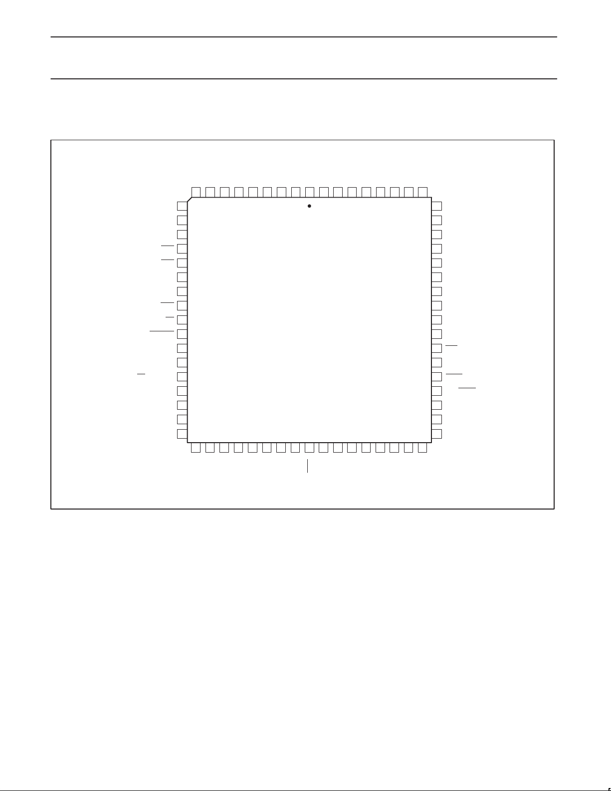
PIN CONFIGURATIONS
68-pin PLCC package
SS
DD
P4.0/ECI
V
AVDDAV
V
SS
P1.0/A0/WRH
XTAL1
37 3828 29
P1.1/A1
XTAL2
P2.7/A19D15
P2.6/A18D14
39 40 41 42 43
P1.3/A3
P1.2/A2
P1.4/RxD1
P4.7/A21
P3.0/RxD0
P3.1/TxD0
P3.2/INT0
P3.3/INT1
P3.4/T0
P3.5/T1/BUSW
P3.6/WRL
P3.7/RD
RSTOUT
V
V
EA/WAIT/V
P5.0/AD0
P5.1/AD1
P5.2/AD2
P5.3/AD3
P4.6/A20
P4.5/CEX4
P4.4/CEX3
P4.3/CEX2
P4.2/CEX1
P4.1/CEX0
765432168 6798 66 65 64 63 62
10
11
12
13
14
15
16
17
18
19
20
SS
21
DD
22
PP
23
24
25
26
27
P5.5/AD5
P5.4/AD4
PLASTIC LEADED CHIP CARRIER
30 31 32 33 34 35 36
REF–
REF+
AV
AV
P5.6/AD6/SCL
P5.7/AD7/SDA
P2.5/A17D13
P2.4/A16D12
P1.6/T2
P1.5/TxD1
P2.3/A15D11
P2.2/A14D10
61
P6.0/A22
P1.7/T2EX
60
P2.1/A13D9
59
P2.0/A12D8
58
P0.7/A11D7
57
P0.6/A10D6
56
P0.5/A9D5
V
55
54
V
P0.4/A8D4
53
P0.3/A7D3
52
51
P0.2/A6D2
RST
50
49
CLKOUT
48
PSEN
ALE/PROG
47
P0.1/A5D1
46
P0.0/A4D0
45
P6.1/A23
44
44
SU00936
SS
DD
XA-S3
2000 Aug 22
3
Page 4
Philips Semiconductors Preliminary specification
XA 16-bit microcontroller
32 K/1 K OTP/ROM/ROMless, 8-channel 8-bit A/D, low voltage (2.7 V–5.5 V),
2
C, 2 UARTs, 16 MB address range
I
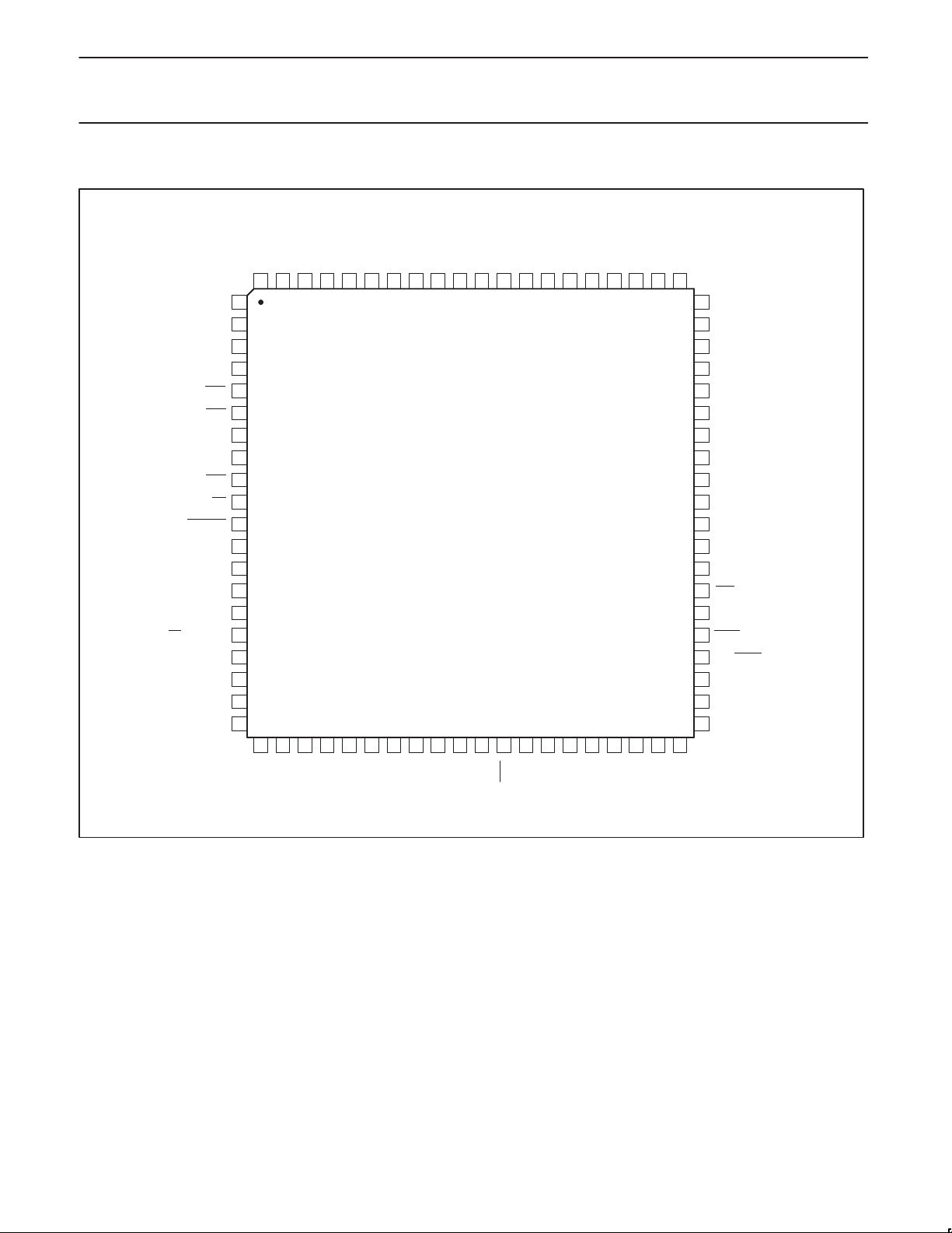
80-pin LQFP package
DD
NC
P4.7/A21
P3.0/RxD0
P3.1/TxD0
P3.2/INT0
P3.3/INT1
P3.4/T0
P3.5/T1/BUSW
P3.6/WRL
P3.7/RD
RSTOUT
V
V
V
V
EA
/WAIT/V
P5.0/AD0
P5.1/AD1
P5.2/AD2
P5.3/AD3
DD
V
P4.0/ECI
P4.1/CEX0
P4.2/CEX1
P4.3/CEX2
P4.4/CEX3
P4.5/CEX4
P4.6/A20
NC
78 77 76 75 74 73 72 71 7080 79 69 68 67 66 65
1
2
3
4
5
6
7
8
9
10
11
12
SS
13
SS
14
DD
15
DD
16
PP
17
18
19
20
NC
P5.4/AD4
LOW PROFILE PLASTIC QUAD FLAT PACK
AVDDAV
30 3121 22
DD
23 24 25 26 27 28 29
REF–
REF+
AV
P5.5/AD5
P5.6/AD6/SCL
AV
P5.7/AD7/SDA
VSSVSSV
32 33 34 35 36
SSAVSS
AV
P1.0/A0/WRH
XTAL1
P1.1/A1
XTAL2
P1.2/A2
P2.7/A19D15
P1.3/A3
P2.4/A16D12
P2.5/A17D13
P2.6/A18D14
64 63 62 61
37 38 39 40
P1.6/T2
P1.5/TxD1
P1.4/RxD1
P2.2/A14D10
P2.3/A15D11
P6.0/A22
P1.7/T2EX
60
NC
59
P2.1/A13D9
58
P2.0/A12D8
57
P0.7/A11D7
56
P0.6/A10D6
P0.5/A9D5
55
54
V
53
V
52
V
V
51
P0.4/A8D4
50
49
P0.3/A7D3
48
P0.2/A6D2
47
RST
CLKOUT
46
PSEN
45
ALE/PROG
44
43
P0.1/A5D1
42
P0.0/A4D0
41
P6.1/A23
SU00937
SS
SS
DD
DD
XA-S3
2000 Aug 22
4
Page 5
Philips Semiconductors Preliminary specification
XA 16-bit microcontroller
32 K/1 K OTP/ROM/ROMless, 8-channel 8-bit A/D, low voltage (2.7 V–5.5 V),
2
C, 2 UARTs, 16 MB address range
I
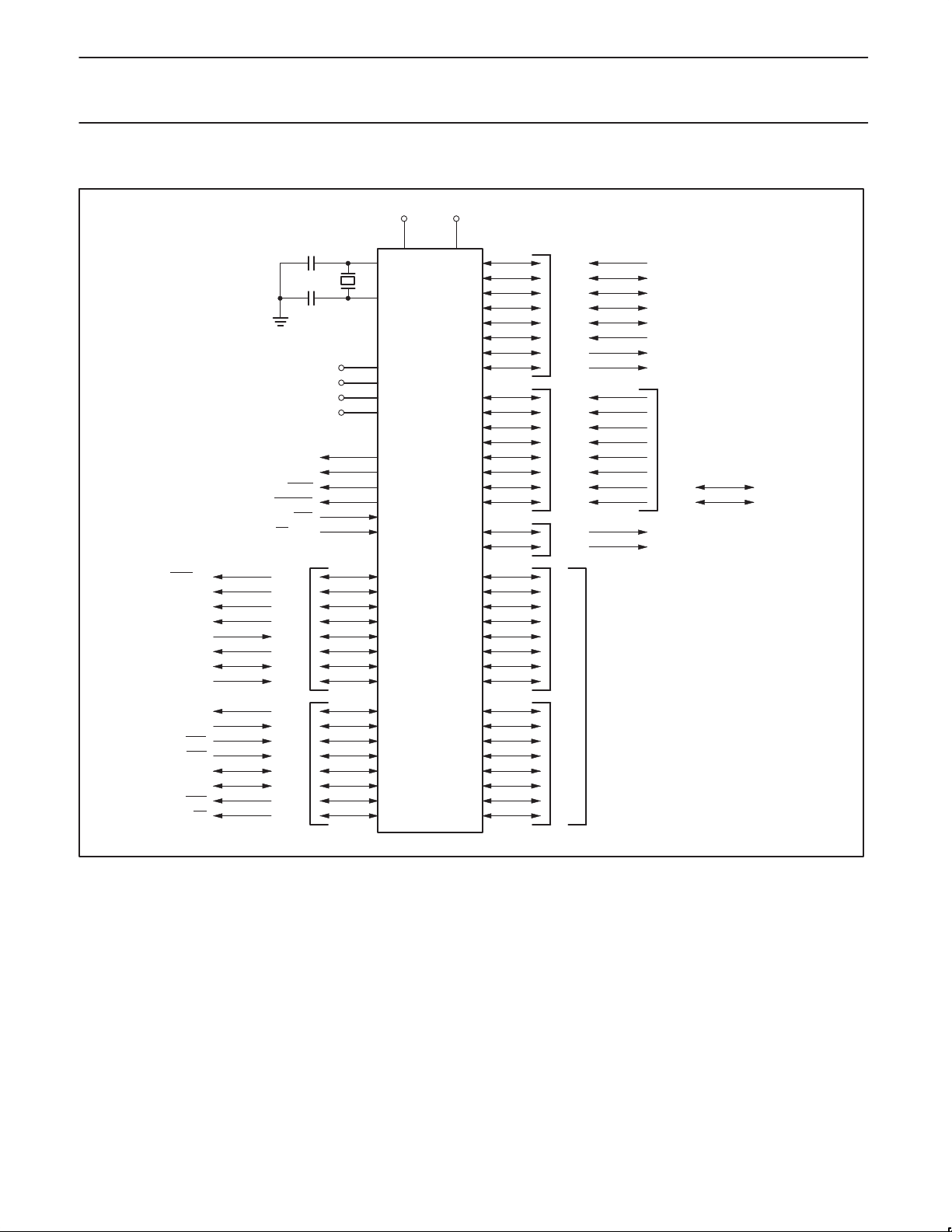
LOGIC SYMBOL
XA-S3
WRH
RxD1
TxD1
T2EX
/A0
A1
A2
A3
V
DD
XTAL1
XTAL2
AV
DD
AV
REF+
AV
REF–
AV
SS
CLKOUT
ALE
PSEN
RSTOUT
RST
EA/WAIT
PORT1PORT3
T2
V
SS
ECI
CEX0
CEX1
CEX2
PORT4PORT5PORT6PORT0PORT2
CEX3
CEX4
A20
A21
INPUTS
A22
A23
A/D
SCL
SDA
RxD0
TxD0
INT0
INT1
T1/BUSW
WRL
ADDRESS AND DATA BUS
T0
RD
SU00847A
2000 Aug 22
5
Page 6
Philips Semiconductors Preliminary specification
XA 16-bit microcontroller
32 K/1 K OTP/ROM/ROMless, 8-channel 8-bit A/D, low voltage (2.7 V–5.5 V),
2
C, 2 UARTs, 16 MB address range
I
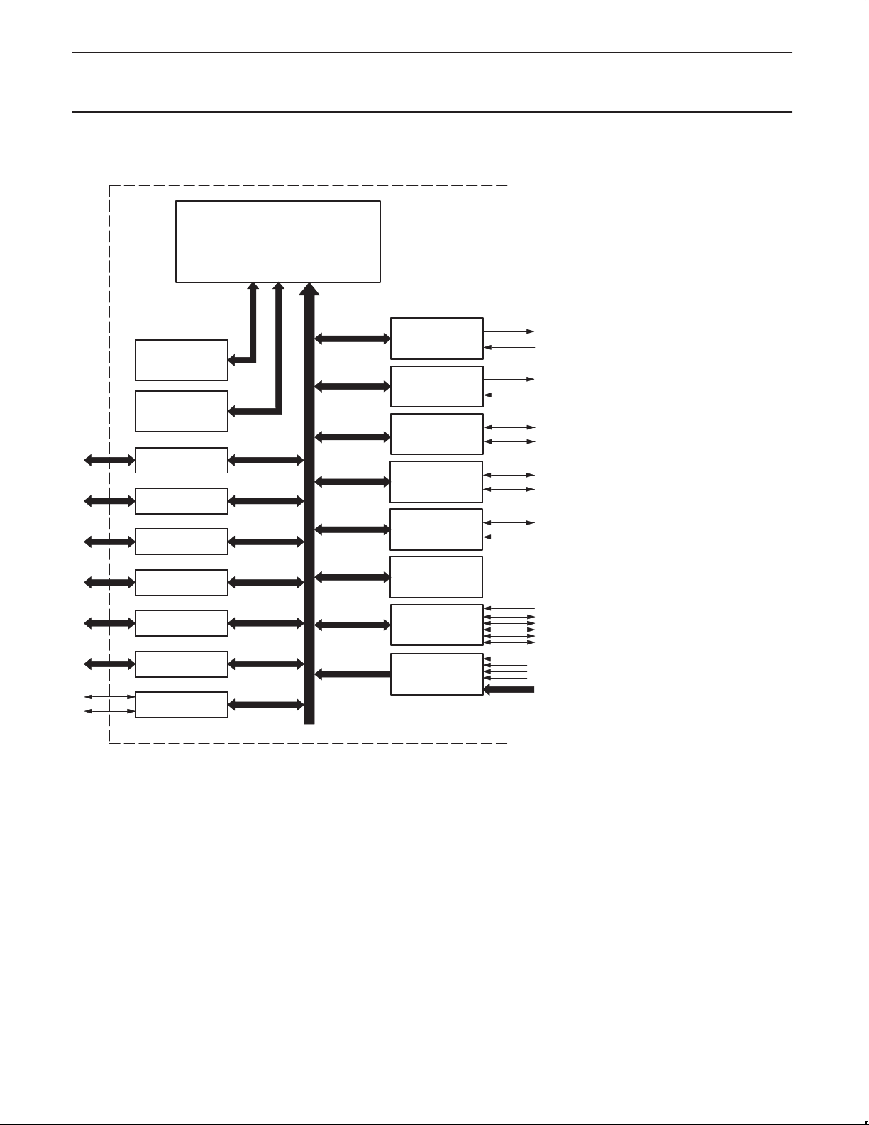
BLOCK DIAGRAM
XA-S3
XA CPU Core
Program
Memory
32K Bytes
ROM/EPROM
1024 Bytes
Static RAM
Port 0
Port 1
Port 2
Port 3
Port 4
Port 5
Port 6
Bus
Data
Bus
SFR
bus
UART 0
UART 1
I2C
Timer 0, 1
Timer 2
Watchdog
Timer
PCA
Input Port/
A/D
2000 Aug 22
SU00846
6
Page 7
Philips Semiconductors Preliminary specification
MNEMONIC
TYPE
NAME AND FUNCTION
XA 16-bit microcontroller
32 K/1 K OTP/ROM/ROMless, 8-channel 8-bit A/D, low voltage (2.7 V–5.5 V),
2
C, 2 UARTs, 16 MB address range
I
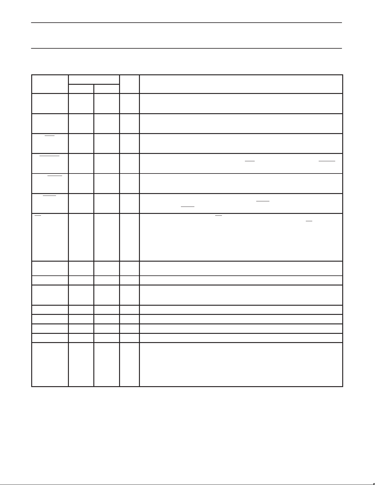
PIN DESCRIPTIONS
PIN NUMBER
PLCC LQFP
V
SS
V
DD
RST 50 47 I Reset: A low on this pin resets the microcontroller, causing I/O ports and peripherals to
RSTOUT 19 11 O Reset Output: This pin outputs a low whenever the XA-S3 processor is reset for any
ALE/PROG 47 44 I/O Address Latch Enable/Program Pulse: A high output on the ALE pin signals external
PSEN 48 45 O Program Store Enable: The read strobe for external program memory. When the
EA/WAIT/V
XTAL1 68 68 I Crystal 1: Input to the inverting amplifier used in the oscillator circuit and input to the
XTAL2 67 67 I Crystal 2: Output from the oscillator amplifier.
CLKOUT 49 46 O Clock Output: This pin outputs a buffered version of the internal CPU clock. The clock
AV
DD
AV
SS
AV
REF+
AV
REF–
P0.0 – P0.7 45, 46,
1, 20, 55 12, 13,
2, 21, 54 14, 15,
PP
22 16 I External Access/Bus W ait: The EA input determines whether the internal program
33 28, 29 I Analog Power Supply: Positive power supply input for the A/D converter.
34 30, 31 I Analog Ground.
32 27 I A/D Positive Reference Voltage: High end reference for the A/D converter.
31 26 I A/D Negative Reference Voltage: Low end reference for the A/D converter.
51–53,
56–58
53, 54,
69, 70
51, 52,
71, 72
42, 43,
48–50,
55–57
I Ground: 0 V reference.
I Power Supply: This is the power supply voltage for normal, idle, and power down
operation.
take on their default states, and the processor to begin execution at the address contained
in the reset vector.
reason. This includes an external reset via the RST pin, watchdog reset, and the RESET
instruction.
circuitry to latch the address portion of the multiplexed address/data bus. A pulse on ALE
occurs only when it is needed in order to process a bus cycle.
microcontroller accesses external program memory, PSEN is driven low in order to enable
memory devices. PSEN
memory of the microcontroller is used for code execution. The value on the EA pin is
latched as the external reset input is released and applies during later execution. When
latched as a 0, external program memory is used exclusively. When latched as a 1, internal
program memory will be used up to its limit, and external program memory used above that
point. After reset is released, this pin takes on the function of bus WAIT input. If WAIT is
asserted high during an external bus access, that cycle will be extended until WAIT is
released.
internal clock generator circuits.
output may be used in conjunction with the external bus to synchronize WAIT state
generators, etc. The clock output may be disabled by software.
I/O Port 0: Port 0 is an 8-bit I/O port with a user-configurable output type. Port 0 latches have
1s written to them and are configured in the quasi-bidirectional mode during reset. The
operation of port 0 pins as inputs and outputs depends upon the port configuration
selected. Each port pin is configured independently. Refer to the section on I/O port
configuration and the DC Electrical Characteristics for details.
When the external program/data bus is used, Port 0 becomes the multiplexed low
data/instruction byte and address lines 4 through 11.
is only active when external code accesses are performed.
XA-S3
2000 Aug 22
7
Page 8
Philips Semiconductors Preliminary specification
XA 16-bit microcontroller
32 K/1 K OTP/ROM/ROMless, 8-channel 8-bit A/D, low voltage (2.7 V–5.5 V),
2
C, 2 UARTs, 16 MB address range
I
XA-S3
MNEMONIC NAME AND FUNCTIONTYPE
MNEMONIC NAME AND FUNCTIONTYPE
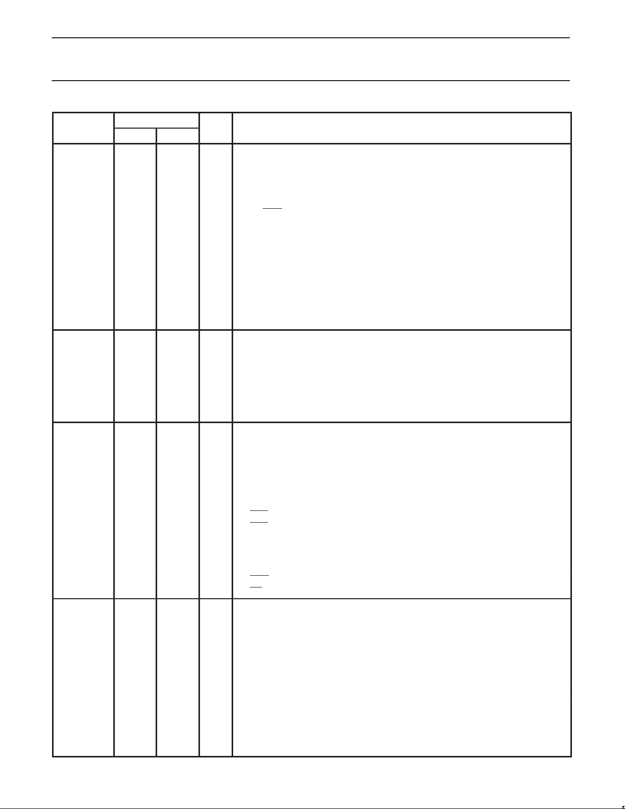
P1.0 – P1.7
P2.0 – P2.7 59–66 58, 59,
P3.0 – P3.7
P4.0 – P4.7
PIN NUMBER
LQFPPLCC
35–42 32–39 I/O Port 1: Port 1 is an 8-bit I/O port with a user-configurable output type. Port 1 latches have
35 32 O A0/WRH (P1.0) Address bit 0 of the external address bus when the eternal data
36 33 O A1 (P1.1): Address bit 1 of the external address bus.
37 34 O A2 (P1.2): Address bit 2 of the external address bus.
38 35 O A3 (P1.3): Address bit 3 of the external address bus.
39 36 I RxD1 (P1.4): Serial port 1 receiver input.
40 37 O TxD1 (P1.5): Serial port 1 transmitter output.
41 38 I/O T2 (P1.6): Timer/counter 2 external count input or overflow output.
42 39 O T2EX (P1.7): Timer/counter 2 reload/capture/direction control.
I/O Port 2: Port 2 is an 8-bit I/O port with a user-configurable output type. Port 2 latches have
61–66
11–18 3–10 I/O Port 3: Port 3 is an 8-bit I/O port with a user-configurable output type. Port 3 latches have
11 3 I RxD0 (P3.0): Receiver input for serial port 0.
12 4 O TxD0 (P3.1): Transmitter output for serial port 0.
13 5 I INT0 (P3.2): External interrupt 0 input.
14 6 I INT1 (P3.3): External interrupt 1 input.
15 7 I/O T0 (P3.4): Timer/counter 0 external count input or overflow output.
16 8 I/O T1 / BUSW (P3.5): Timer/counter 1 external count input or overflow output. The
17 9 O WRL (P3.6): External data memory low byte write strobe.
18 10 O RD (P3.7): External data memory read strobe.
3–10 73–79, 2 I/O Port 4: Port 4 is an 8-bit I/O port with a user-configurable output type. Port 4 latches have
3 73 I ECI (P4.0): PCA External clock input.
4 74 I/O CEX0 (P4.1): Capture/compare external I/O for PCA module 0.
5 75 I/O CEX1 (P4.2): Capture/compare external I/O for PCA module 1.
6 76 I/O CEX2 (P4.3): Capture/compare external I/O for PCA module 2.
7 77 I/O CEX3 (P4.4): Capture/compare external I/O for PCA module 3.
8 78 I/O CEX4 (P4.5): Capture/compare external I/O for PCA module 4.
9 79 O A20 (P4.6): Address bit 20 of the external address bus.
10 2 O A21 (P4.7): Address bit 21 of the external address bus.
1s written to them and are configured in the quasi-bidirectional mode during reset. The
operation of port 1 pins as inputs and outputs depends upon the port configuration
selected. Each port pin is configured independently. Refer to the section on I/O port
configuration and the DC Electrical Characteristics for details.
Port 1 also provides various special functions as described below:
bus is configured for an 8-bit width. When the external data bus
is configured for a 16-bit width, this pin becomes the high byte
write strobe.
1s written to them and are configured in the quasi-bidirectional mode during reset. The
operation of port 2 pins as inputs and outputs depends upon the port configuration
selected. Each port pin is configured independently. Refer to the section on I/O port
configuration and the DC Electrical Characteristics for details.
When the external program/data bus is used in 16-bit mode, Port 2 becomes the
multiplexed high data/instruction byte and address lines 12 through 19. When the external
data/address bus is used in 8-bit mode, the number of address lines that appear on Port 2
is user programmable in groups of 4 bits.
1s written to them and are configured in the quasi-bidirectional mode during reset. The
operation of port 3 pins as inputs and outputs depends upon the port configuration
selected. Each port pin is configured independently. Refer to the section on I/O port
configuration and the DC Electrical Characteristics for details.
Port 3 also provides the various special functions as described below:
value on this pin is latched as an external chip reset is
completed and defines the default external data bus width.
1s written to them and are configured in the quasi-bidirectional mode during reset. The
operation of Port 4 pins as inputs and outputs depends upon the port configuration
selected. Each port pin is configured independently. Refer to the section on I/O port
configuration and the DC Electrical Characteristics for details.
Port 4 also provides various special functions as described below:
2000 Aug 22
8
Page 9
Philips Semiconductors Preliminary specification
XA 16-bit microcontroller
32 K/1 K OTP/ROM/ROMless, 8-channel 8-bit A/D, low voltage (2.7 V–5.5 V),
2
C, 2 UARTs, 16 MB address range
I
XA-S3
MNEMONIC NAME AND FUNCTIONTYPE
MNEMONIC NAME AND FUNCTIONTYPE
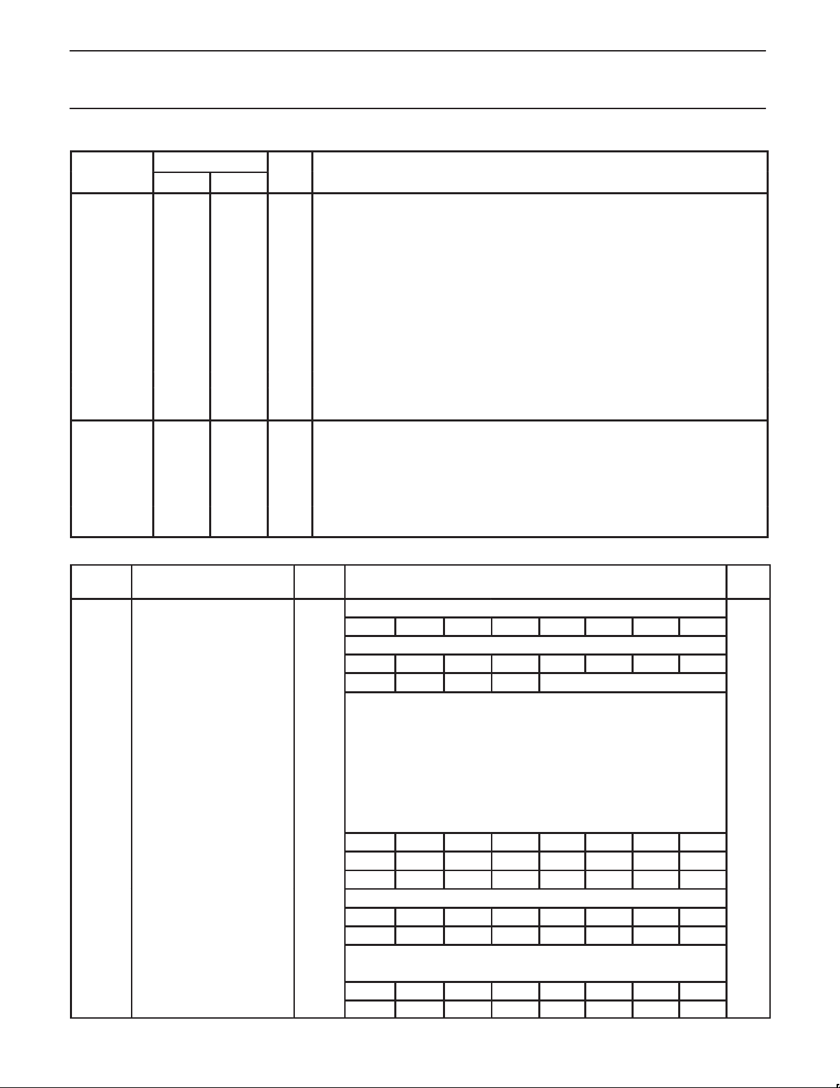
P5.0 – P5.7
P6.0 – P6.7
PIN NUMBER
LQFPPLCC
23–30 17–20,
22–25
23 17 I AD0 (P5.0): A/D channel 0 input.
24 18 I AD1 (P5.1): A/D channel 1 input.
25 19 I AD2 (P5.2): A/D channel 2 input.
26 20 I AD3 (P5.3): A/D channel 3 input.
27 22 I AD4 (P5.4): A/D channel 4 input.
28 23 I AD5 (P5.5): A/D channel 5 input.
29 24 I/O AD6/SCL (P5.6): A/D channel 6 input. I2C serial clock input/output.
30 25 I/O AD7/SDA (P5.7): A/D channel 7 input. I2C serial data input/output.
43, 44 40, 41 I/O Port 6: Port 6 is a 2-bit I/O port with a user-configurable output type. Port 6 latches have
43 40 O A22 (P6.0): Address bit 22 of the external address bus.
44 41 O A23 (P6.1): Address bit 23 of the external address bus.
I/O Port 5: Port 5 is an 8-bit I/O port with a user-configurable output type. Port 5 latches have
1s written to them and are configured in the quasi-bidirectional mode during reset. The
operation of Port 5 pins as inputs and outputs depends upon the port configuration
selected. Each port pin is configured independently. Refer to the section on I/O port
configuration and the DC Electrical Characteristics for details.
Port 5 also provides various special functions as described below. Port 5 pins used as A/D
inputs must be configured by the user to the high impedance mode.
1s written to them and are configured in the quasi-bidirectional mode during reset. The
operation of Port 6 pins as inputs and outputs depends upon the port configuration
selected. Each port pin is configured independently. Refer to the section on I/O port
configuration and the DC Electrical Characteristics for details.
Port 6 also provides special functions as described below:
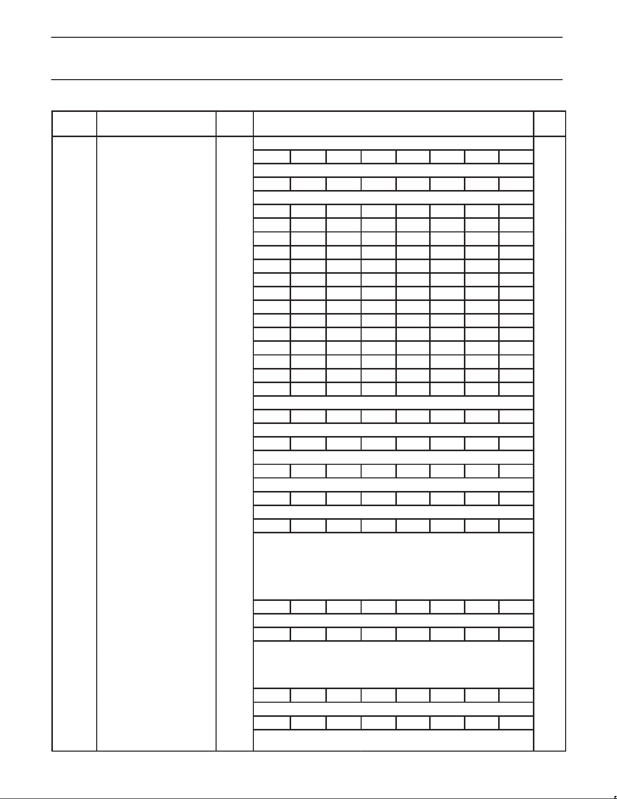
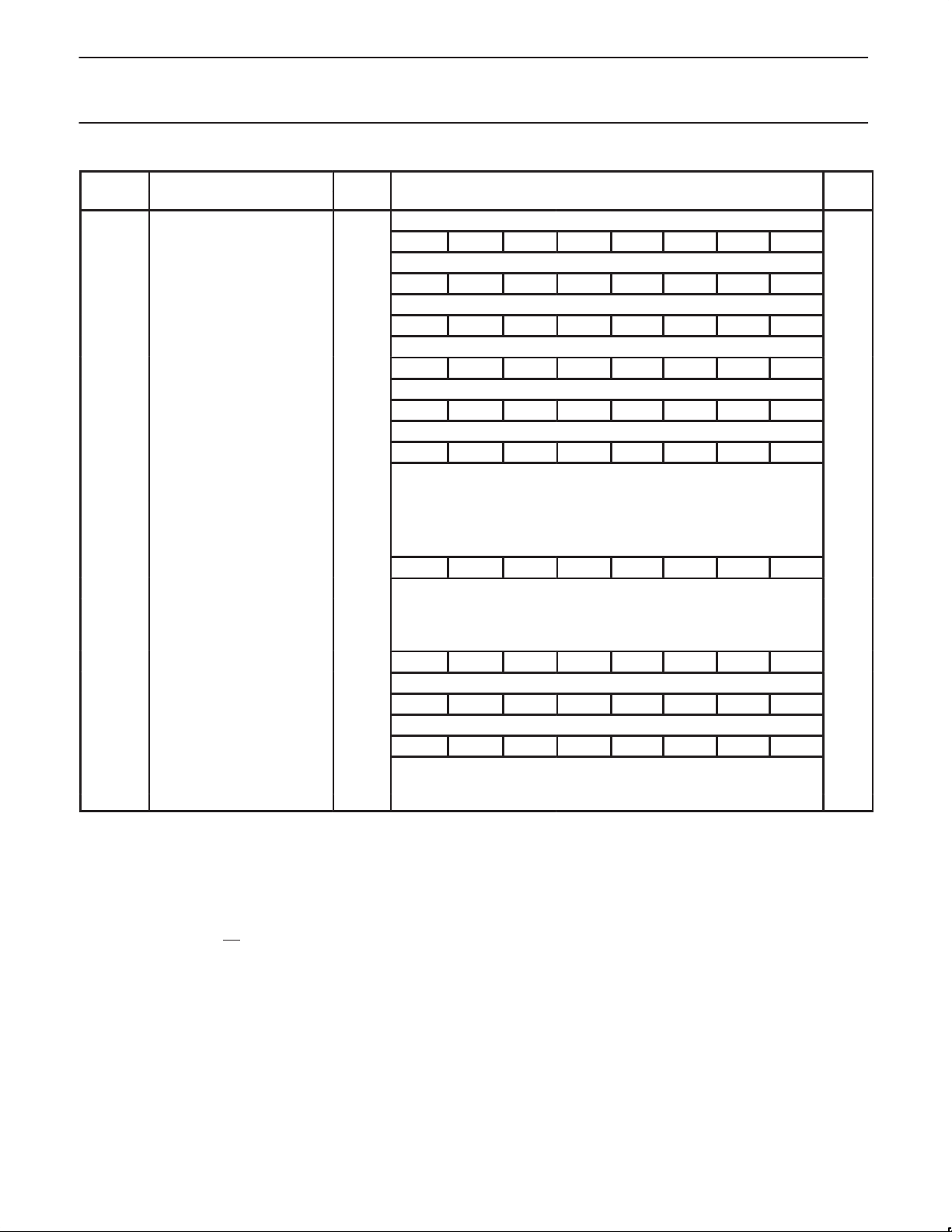
Table 1. Special Function Registers
SFR
NAME DESCRIPTION
ADCON#* A/D control register 43E – – – –
ADCS#* A/D channel select register 43F
ADCFG# A/D timing configuration 4B9 – – – – A/D Timing Configuration 0Fh
ADRSH0# A/D high byte result, channel 0 4B0 xx
ADRSH1# A/D high byte result, channel 1 4B1 xx
ADRSH2# A/D high byte result, channel 2 4B2 xx
ADRSH3# A/D high byte result, channel 3 4B3 xx
ADRSH4# A/D high byte result, channel 4 4B4 xx
ADRSH5# A/D high byte result, channel 5 4B5 xx
ADRSH6# A/D high byte result, channel 6 4B6 xx
ADRSH7# A/D high byte result, channel 7 4B7 xx
ADRSL# Two LSBs of 10-bit A/D result 4B8 xx
BCR# Bus configuration register 46A – – CLKD WAITD BUSD BC2 BC1 BC0 Note 1
BTRH Bus timing register high byte 469 DW1 DW0 DWA1 DWA0 DR1 DR0 DRA1 DRA0 FFh
BTRL Bus timing register low byte 468 WM1 WM0 ALEW – CR1 CR0 CRA1 CRA0 EFh
CCON#* PCA counter control 41A CF CR – CCF4 CCF3 CCF2 CCF1 CCF0 00h
CMOD# PCA mode control 490 CIDL WDTE – – – CPS1 CPS0 ECF 00h
CH# PCA counter high byte 48B 00h
CL# PCA counter low byte 48A 00h
CCAPM0# PCA module 0 mode 491 – ECOM0 CAPP0 CAPN0 MAT0 TOG0 PWM0 ECCF0 00h
CCAPM1# PCA module 1 mode 492 – ECOM1 CAPP1 CAPN1 MAT1 TOG1 PWM1 ECCF1 00h
Address
MSB LSB Value
3F7 3F6 3F5 3F4 3F3 3F2 3F1 3F0
3FF 3FE 3FD 3FC 3FB 3FA 3F9 3F8
ADCS7 ADCS6 ADCS5 ADCS4 ADCS3 ADCS2 ADCS1 ADCS0
2D7 2D6 2D5 2D4 2D3 2D2 2D1 2D0
BIT FUNCTIONS AND ADDRESSES Reset
ADRES ADMOD ADSST ADINT
00h
00h
2000 Aug 22
9
Page 10
Philips Semiconductors Preliminary specification
XA 16-bit microcontroller
32 K/1 K OTP/ROM/ROMless, 8-channel 8-bit A/D, low voltage (2.7 V–5.5 V),
2
C, 2 UARTs, 16 MB address range
I
XA-S3
SFR
NAME ValueLSBMSB
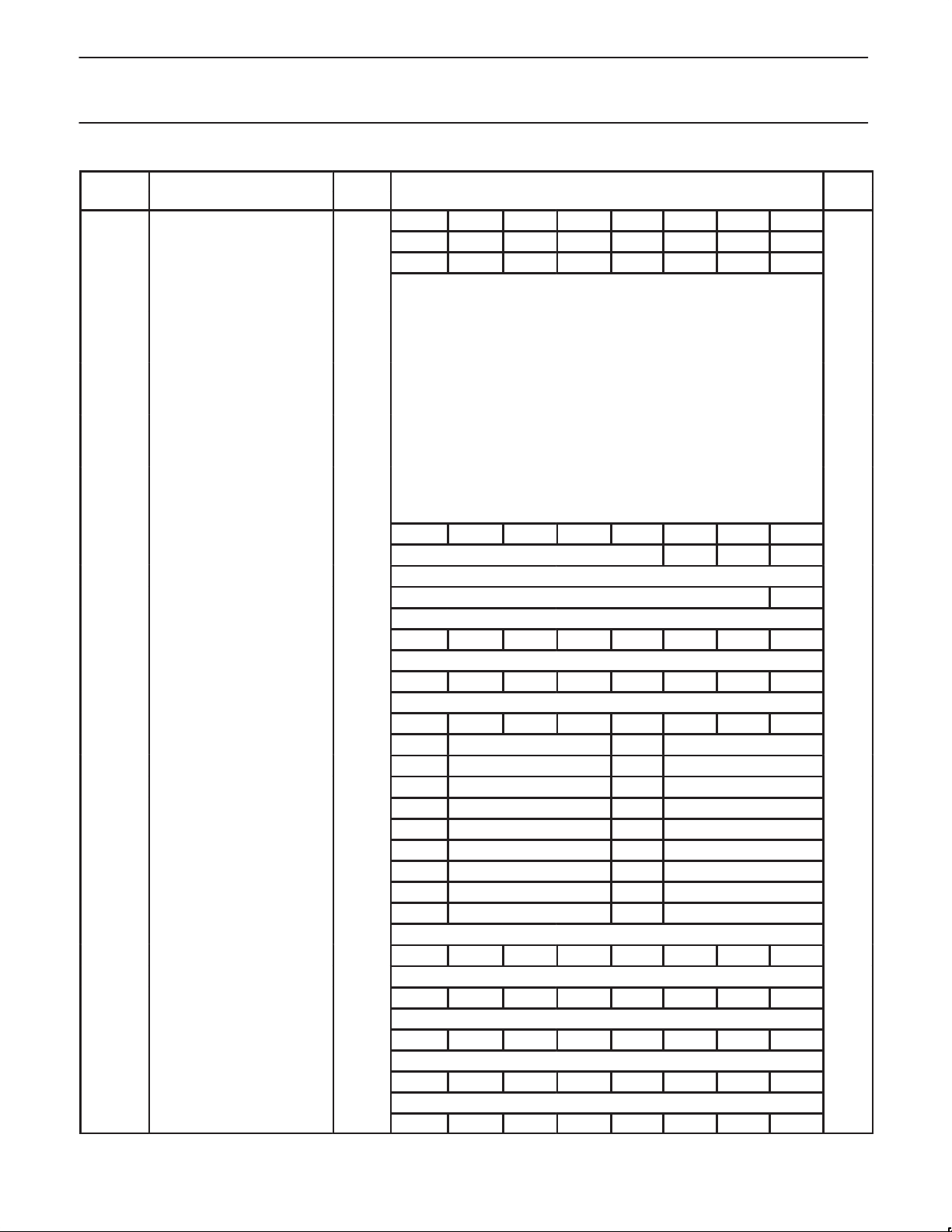
CCAPM2# PCA module 2 mode 493 – ECOM2 CAPP2 CAPN2 MAT2 TOG2 PWM2 ECCF2 00h
CCAPM3# PCA module 3 mode 494 – ECOM3 CAPP3 CAPN3 MAT3 TOG3 PWM3 ECCF3 00h
CCAPM4# PCA module 4 mode 495 – ECOM4 CAPP4 CAPN4 MAT4 TOG4 PWM4 ECCF4 00h
CCAP0H# PCA module 0 capture high byte 497 xx
CCAP1H# PCA module 1 capture high byte 499 xx
CCAP2H# PCA module 2 capture high byte 49B xx
CCAP3H# PCA module 3 capture high byte 49D xx
CCAP4H# PCA module 4 capture high byte 49F xx
CCAP0L# PCA module 0 capture low byte 496 xx
CCAP1L# PCA module 1 capture low byte 498 xx
CCAP2L# PCA module 2 capture low byte 49A xx
CCAP3L# PCA module 3 capture low byte 49C xx
CCAP4L# PCA module 4 capture low byte 49E xx
CS Code segment 443 00h
DS Data segment 441 00h
ES Extra segment 442 00h
I2CON#* I2C control register 42C CR2 ENA STA STO SI AA CR1 CR0 00h
I2STAT# I2C status register 46C I2C Status Code/Vector 0 0 0 F8h
I2DAT# I2C data register 46D xx
I2ADDR# I2C address register 46E I2C Slave Address GC 00h
IEH* Interrupt enable high byte 427 – – – – ETI1 ERI1 ETI0 ERI0 00h
IEL#* Interrupt enable low byte 426 EA EAD EPC ET2 ET1 EX1 ET0 EX0 00h
IELB#* Interrupt enable B low byte 42E – – EI2 EC4 EC3 EC2 EC1 EC0 00h
IPA0 Interrupt priority A0 4A0 – PT0 – PX0 00h
IPA1 Interrupt priority A1 4A1 – PT1 – PX1 00h
IPA2# Interrupt priority A2 4A2 – PPC – PT2 00h
IPA3# Interrupt priority A3 4A3 – – – PAD 00h
IPA4 Interrupt priority A4 4A4 – PTI0 – PRI0 00h
IPA5 Interrupt priority A5 4A5 – PTI1 – PRI1 00h
IPB0# Interrupt priority B0 4A8 – PC1 – PC0 00h
IPB1# Interrupt priority B1 4A9 – PC3 – PC2 00h
IPB2# Interrupt priority B2 4AA – PI2 – PC4 00h
P0* Port 0 430 A11D7 A10D6 A9D5 A8D4 A7D3 A6D2 A5D1 A4D0 FFh
P1* Port 1 431 T2EX T2 TxD1 RxD1 A3 A2 A1
P2* Port 2 432
P3* Port 3 433 RD WRL T1 T0 INT1 INT0 TxD0 RxD0 FFh
P4#* Port 4 434 A21 A20 CEX4 CEX3 CEX2 CEX1 CEX0 ECI FFh
DESCRIPTION
Address
367 366 365 364 363 362 361 360
33F 33E 33D 33C 33B 33A 339 338
337 336 335 334 333 332 331 330
377 376 375 374 373 372 371 370
387 386 385 384 383 382 381 380
38F 38E 38D 38C 38B 38A 389 388
A0/WRH
397 396 395 394 393 392 391 390
A19D15 A18D14 A17D13 A16D12 A15D11 A14D10 A13D9 A12D8
39F 39E 39D 39C 39B 39A 399 398
3A7 3A6 3A5 3A4 3A3 3A2 3A1 3A0
ResetBIT FUNCTIONS AND ADDRESSES
FFh
FFh
2000 Aug 22
10
Page 11
Philips Semiconductors Preliminary specification
XA 16-bit microcontroller
32 K/1 K OTP/ROM/ROMless, 8-channel 8-bit A/D, low voltage (2.7 V–5.5 V),
2
C, 2 UARTs, 16 MB address range
I
XA-S3
SFR
NAME ValueLSBMSB
P5#* Port 5 435
P6#* Port 6 436 – – – – – – A23 A22 FFh
P0CFGA Port 0 configuration A 470 Note 5
P1CFGA Port 1 configuration A 471 Note 5
P2CFGA Port 2 configuration A 472 Note 5
P3CFGA Port 3 configuration A 473 Note 5
P4CFGA# Port 4 configuration A 474 Note 5
P5CFGA# Port 5 configuration A 475 Note 5
P6CFGA# Port 6 configuration A 476 – – – – – – Note 5
P0CFGB Port 0 configuration B 4F0 Note 5
P1CFGB Port 1 configuration B 4F1 Note 5
P2CFGB Port 2 configuration B 4F2 Note 5
P3CFGB Port 3 configuration B 4F3 Note 5
P4CFGB# Port 4 configuration B 4F4 Note 5
P5CFGB# Port 5 configuration B 4F5 Note 5
P6CFGB# Port 6 configuration B 4F6 – – – – – – Note 5
PCON* Power control register 404 – – – – – – PD IDL 00h
PSWH* Program status word (high byte) 401 SM TM RS1 RS0 IM3 IM2 IM1 IM0 Note 2
PSWL* Program status word (low byte) 400 C AC – – – V N Z Note 2
PSW51* 80C51 compatible PSW 402 C AC F0 RS1 RS0 V F1 P Note 3
DESCRIPTION
Address
3AF 3AE 3AD 3AC 3AB 3AA 3A9 3A8
AD7/SDA AD6/SCL
227 226 225 224 223 222 221 220
20F 20E 20D 20C 20B 20A 209 208
207 206 205 204 203 202 201 200
217 216 215 214 213 212 211 210
AD5 AD4 AD3 AD2 AD1 AD0 FFh
3B1 3B0
ResetBIT FUNCTIONS AND ADDRESSES
RSTSRC# Reset source register 463 – – – – – R_WD
RTH0 Timer 0 reload register, high byte 455 00h
RTH1 Timer 1 reload register, high byte 457 00h
RTL0 Timer 0 reload register, low byte 454 00h
RTL1 Timer 1 reload register, low byte 456 00h
307 306 305 304 303 302 301 300
S0CON* Serial port 0 control reg ister 420 SM0_0 SM1_0 SM2_0 REN_0 TB8_0 RB8_0 TI_0 RI_0 00h
30F 30E 30D 30C 30B 30A 309 308
S0STAT#* Serial port 0 extended status 421 – – – ERR0 FE0 BR0 OE0
S0BUF Serial port 0 data buffer register 460 xx
S0ADDR Serial port 0 address register 461 00h
S0ADEN Serial port 0 address enable 462 00h
327 326 325 324 323 322 321 320
S1CON* Serial port 1 control register 424 SM0_1 SM1_1 SM2_1 REN_1 TB8_1 RB8_1 TI_1 RI_1 00H
32F 32E 32D 32C 32B 32A 329 328
S1STAT#* Serial port 1 extended status 425 – – – ERR1 FE1 BR1 OE1
S1BUF Serial port 1 data buffer register 464 xx
S1ADDR Serial port 1 address register 465 00h
2000 Aug 22
11
R_CMD
R_EXT Note 7
STINT0
STINT1
00h
00h
Page 12
Philips Semiconductors Preliminary specification
XA 16-bit microcontroller
32 K/1 K OTP/ROM/ROMless, 8-channel 8-bit A/D, low voltage (2.7 V–5.5 V),
2
C, 2 UARTs, 16 MB address range
I
XA-S3
SFR
NAME ValueLSBMSB
S1ADEN Serial port 1 address enable 466 00h
SCR System configuration register 440 – – – – PT1 PT0 CM PZ 00h
SSEL* Segment selection register 403
SWE Software interrupt enable 47A – SWE7 SWE6 SWE5 SWE4 SWE3 SWE2 SWE1 00h
SWR* Software interrupt request 42A – SWR7 SWR6 SWR5 SWR4 SWR3 SWR2 SWR1 00h
T2CON* Timer 2 control register 418 TF2 EXF2 RCLK0 TCLK0
T2MOD* Timer 2 mode control 419 – – RCLK1 TCLK1 – – T2OE DCEN 00h
TH2 Timer 2 high byte 459 00h
TL2 Timer 2 low byte 458 00h
T2CAPH T imer 2 capture, high byte 45B 00h
T2CAPL Timer 2 capture, low byte 45A 00h
TCON* Timer 0 and 1 control register 410 TF1 TR1 TF0 TR0 IE1 IT1 IE0 IT0 00h
TH0 Timer 0 high byte 451 00h
TH1 Timer 1 high byte 453 00h
TL0 Timer 0 low byte 450 00h
TL1 Timer 1 low byte 452 00h
TMOD Timer 0 and 1 mode cont rol 45C GATE C/T M1 M0 GATE C/T M1 M0 00h
TSTAT* Timer 0 and 1 extended status 411 – – – – – T1OE – T0OE 00h
WDCON* Watchdog control register 41F PEW2 PRE1 PRE0 – –
WDL Watchdog timer reload 45F 00h
WFEED1 Watchdog feed 1 45D xx
WFEED2 Watchdog feed 2 45E xx
NOTES:
* SFRs are bit addressable.
# SFRs are modified from or added to XA-G3 SFRs.
1. At reset, the BCR is loaded with the binary value 00000a11, where “a’ is the value on the BUSW pin. This defaults the address bus size to 24 bits.
2. SFR is loaded from the reset vector.
3. All bits except F1, F0, and P are loaded from the reset vector. Those bits are all 0.
4. Unimplemented bits in SFRs are X (unknown) at all times. Ones should not be written to these bits since they may be used for other
purposes in future XA derivatives. The reset value shown for these bits is 0.
5. Port configurations default to quasi-bidirectional when the XA begins execution from internal code memory after reset, based on the
condition found on the EA
execution using internal code memory. When the XA begins execution using external code memory, the default configuration for pins that
are associated with the external bus will be push-pull. The PnCFGA and PnCFGB register contents will reflect this difference.
6. The WDCON reset value is E6 for a Watchdog reset, E4 for all other reset causes.
7. The RSTSRC register reflects the cause of the last XA-S3 reset. One bit will be set to 1, the others will be cleared to 0.
8. The XA guards writes to certain bits (typically interrupt flags) that may be altered directly by a peripheral function. This prevents loss of an
interrupt or other status if a bit was written directly by a peripheral action during the time between the read and write portions of an
instruction that performs a read-modify-write operation. Examples of such instructions are:
XA-S3 SFR bits that are guarded in this manner are: ADINT (in ADCON); CF, CCF4, CCF3, CCF2, CCF1, and CCF0 (in CCON); SI (in
I2CON); TI_0 and RI_0 (in S0CON); TI_1 and RI_1 (in S1CON); FE0, BR0, and OE0 (in S0STAT); FE1, BR1, and OE1 (in S1STAT); TF2 (in
T2CON); TF1, TF0, IE1, and IE0 (in TCON); and WDTOF (in WDCON).
9. The XA-S3 implements an 8-bit SFR bus, as stated in
to write 16 bits to an SFR will actually write only the lower 8 bits. Sixteen bit SFR reads will return undefined data in the upper byte.
DESCRIPTION
pin. Thus, all PnCFGA registers will contain FF, and PnCFGB register will contain 00 when the XA begins
and s0con,#$fb
clr tr0
setb ti_0
Address
21F 21E 21D 21C 21B 21A 219 218
ESWEN R6SEG R5SEG R4SEG R3SEG R2SEG R1SEG R0SEG
357 356 355 354 353 352 351 350
2C7 2C6 2C5 2C4 2C3 2C2 2C1 2C0
EXEN2
2CF 2CE 2CD 2CC 2CB 2CA 2C9 2C8
287 286 285 284 283 282 281 280
28F 28E 28D 28C 28B 28A 289 288
2FF 2FE 2FD 2FC 2FB 2FA 2F9 2F8
Chapter 8
of the
XA User Guide
. All SFR accesses must be 8-bit operations. Attempts
TR2 C/T2
WDRUN WDTOF
CP/RL2
ResetBIT FUNCTIONS AND ADDRESSES
00h
00h
– Note 6
2000 Aug 22
12
Page 13
Philips Semiconductors Preliminary specification
XA 16-bit microcontroller
32 K/1 K OTP/ROM/ROMless, 8-channel 8-bit A/D, low voltage (2.7 V–5.5 V),
2
C, 2 UARTs, 16 MB address range
I
FFFFFh
Up to 16 MB
Total Code
Memory
8000h
7FFFh
32 kB On-chip
Code Memory
0000h
SU01219
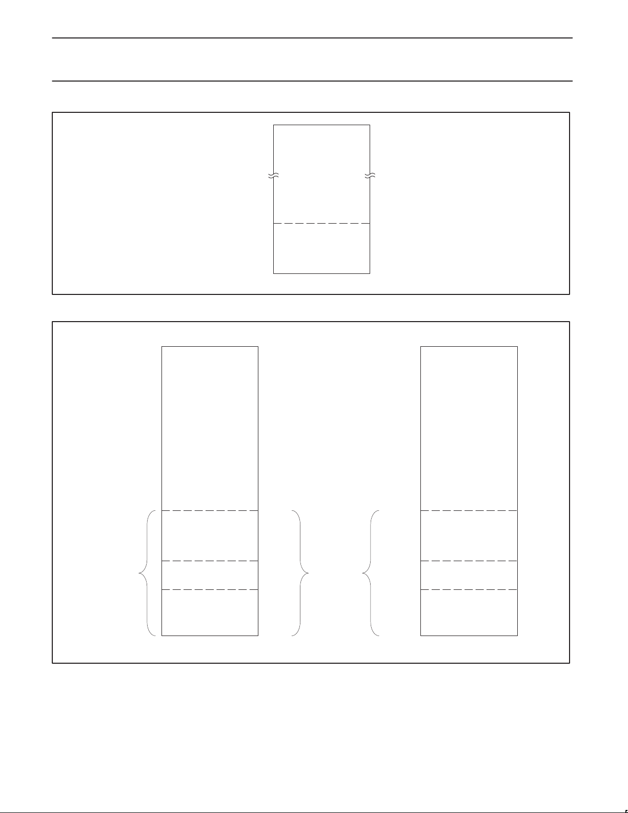
Figure 1. XA-S3 program memory map
XA-S3
1 kB
On-Chip Data
Memory
(RAM)
Data Segment 0
Data Memory
(Indirectly Addressed,
Off-Chip)
Data Memory
(Directly or Indirectly
Addressable, On-Chip
(Bit-Addressable
Data Area)
Data Memory
(Directly or Indirectly
Addressable, On-Chip
FFFFh
0400h
03FFh
0040h
003Fh
0020h
001Fh
0000h
Directly
Addressed
Data
(1 k per
Segment)
FFFFh
0400h
03FFh
0040h
003Fh
0020h
001Fh
0000h
Other Data Segments
Data Memory
(Indirectly Addressed,
Off-Chip)
Data Memory
(Directly or Indirectly
Addressable, On-Chip
(Bit-Addressable
Data Area)
Data Memory
(Directly or Indirectly
Addressable, Off-Chip
2000 Aug 22
SU01220
Figure 2. XA-S3 data memory map
13
Page 14

Philips Semiconductors Preliminary specification
XA 16-bit microcontroller
32 K/1 K OTP/ROM/ROMless, 8-channel 8-bit A/D, low voltage (2.7 V–5.5 V),
2
C, 2 UARTs, 16 MB address range
I
XA-S3
FUNCTIONAL DESCRIPTION
Details of XA-S3 functions will be described in the following sections.
Analog to Digital converter
The XA-S3 has an 8-channel, 8-bit A/D converter with 8 sets of result
registers, single scan and multiple scan operating modes. The A/D
also has a 10-bit conversion mode that provides greater result
resolution. The A/D input range is limited to 0 to AV
The A/D inputs are on Port 5. Analog Power and Ground as well as
AV
and AV
REF+
be used. Prior to enabling the A/D converter or driving analog signals
into the A/D inputs, the port configurations for the pins being used as
A/D inputs must be set to the “off” (high impedance, input only) mode.
A/D timing can be adapted to the application clock frequency in
order to provide the fastest possible conversion.
A/D converter operation is controlled through the ADCON (A/D Control)
register, see Figure 1. Bits in ADCON start and stop the A/D, flag
conversion completion, and select the converter operating modes. When
10-bit resolution is needed, the A/D mode may be set to give 10 result
bits by setting the ADRES bit to 1. In this mode, the A/D takes longer to
complete a conversion, and the timing must be set differently in ADCFG.
A/D Conversion Modes
The A/D converter supports a single scan mode and a continuous
scan mode. In either mode, one or more A/D channels may be
converted. The ADCS register determines which channels are
converted. If the corresponding bit in the ADCS register is set, that
channel is selected for conversions, otherwise that channel is
skipped. The ADCS register is detailed in Figure 2.
For any A/D conversion, the results are stored in ADRSHn,
corresponding to the A/D channel just converted. For a 10-bit
conversion, the two least significant bits are read from the upper end
must be supplied in order for the A/D converter to
REF–
(3.3 V max.).
DD
of register ADRSL. These bits must be read before another
conversion is begun.
A/D conversions are begun by setting the A/D Start and STatus bit in
ADCON. In the single scan mode, all of the channels selected by
bits in the ADCS register will be converted once. The ADINT flag is
set when the last channel is converted. In the continuous scan
mode, the A/D converter continuously converts all A/D channels
selected by bits in the ADCS register. The ADINT flag is set when all
channels have been converted once.
The A/D converter can generate an interrupt when the ADINT flag is
set. This will occur if the A/D interrupt is enabled (via the EAD bit in
IEL), the interrupt system is enabled (via the EA bit in IEL), and the
A/D interrupt priority (specified in IPA3 bits 3 to 0) is higher than the
currently running code (PSW bits IM3 through IM0) and any other
pending interrupt. ADINT must be cleared by software.
A/D Timing Configuration
The A/D sampling and conversion timing may be optimized for the
particular oscillator frequency and input drive characteristics of the
application. Because A/D operation is mostly dependent on real-time
effects (charging time of sampling capacitors, settling time of the
comparator, etc.), A/D conversion times are not necessarily much
longer at slower clock frequencies. The A/D timing is controlled by
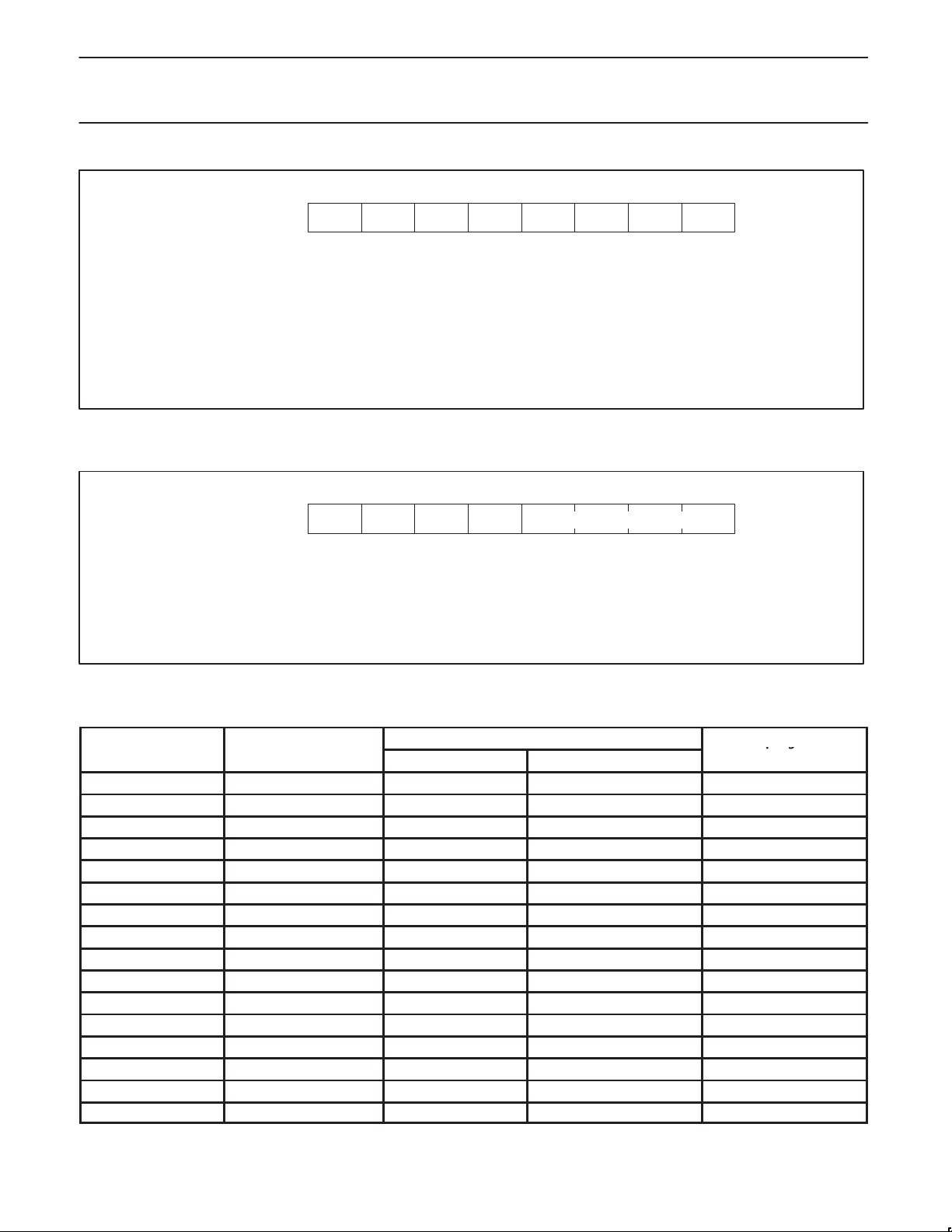
the ADCFG register, as shown in Figure 3, Table 2 and Table 3.
The primary effect of ADCFG settings is to adjust the A/D sample
and hold time to be relatively constant over various clock
frequencies. Two settings (value 6 and B) are provided to allow fast
conversions with a lower external source driving the A/D inputs.
These settings provide double the sample time at the same
frequency. Of course, settings intended for lower frequencies may
also be used at higher frequencies in order to increase the A/D
sampling time, but this method has the side effect of significantly
increasing A/D conversion times.
ADCON Address:43Eh
Bit Addressable
Reset Value: 00h
BIT SYMBOL FUNCTION
ADCON.7 — Reserved for future use. Should not be set to 1 by user programs.
ADCON.6 — Reserved for future use. Should not be set to 1 by user programs.
ADCON.5 — Reserved for future use. Should not be set to 1 by user programs.
ADCON.4 — Reserved for future use. Should not be set to 1 by user programs.
ADCON.3 ADRES Selects 8-bit (0) or 10-bit (1) conversion mode.
ADCON.2 ADMOD A/D mode select.
1 = continuous scan of selected inputs after a start of the A/D.
0 = single scan of selected inputs after a start of the A/D.
ADCON.1 ADSST A/D start and status. Setting this bit by software starts the A/D conversion of the selected A/D
inputs. ADSST remains set as long as the A/D is in operation. In continuous conversion mode,
ADSST will remain set unless the A/D is stopped by software. While ADSST is set, new start
commands are ignored. An A/D conversion is progress may be aborted by software clearing
ADSST.
ADCON.0 ADINT A/D conversion complete/interrupt flag. This flag is set when all selected A/D channels are
converted in either the single scan or continuous scan modes. Must be cleared by software.
Figure 1. A/D Control Register (ADCON)
ADSSTADMODADRES————
LSBMSB
ADINT
SU01229
2000 Aug 22
14
Page 15
Philips Semiconductors Preliminary specification
ADCFG.3–0
pg
XA 16-bit microcontroller
32 K/1 K OTP/ROM/ROMless, 8-channel 8-bit A/D, low voltage (2.7 V–5.5 V),
2
C, 2 UARTs, 16 MB address range
I
XA-S3
ADCS Address:43Fh
Bit Addressable
Reset Value: 00h
BIT SYMBOL FUNCTION
ADCS.7 ADCS7 A/D channel 7 select bit.
ADCS.6 ADCS6 A/D channel 6 select bit.
ADCS.5 ADCS5 A/D channel 5 select bit.
ADCS.4 ADCS4 A/D channel 4 select bit.
ADCS.3 ADCS3 A/D channel 3 select bit.
ADCS.2 ADCS2 A/D channel 2 select bit.
ADCS.1 ADCS1 A/D channel 1 select bit.
ADCS.0 ADCS0 A/D channel 0 select bit.
Figure 2. A/D Channel Select Register (ADCS)
ADCFG Address:4B9h
Not bit Addressable
Reset Value: 00h
BIT SYMBOL FUNCTION
ADCFG.7 — Reserved for future use. Should not be set to 1 by user programs.
ADCFG.6 — Reserved for future use. Should not be set to 1 by user programs.
ADCFG.5 — Reserved for future use. Should not be set to 1 by user programs.
ADCFG.4 — Reserved for future use. Should not be set to 1 by user programs.
ADCFG.3–0 ADCFG A/D timing configuration (see text and table).
Figure 3. A/D Timing Configuration Register (ADCFG)
A/D Timing Configuration————
LSBMSB
ADCS1ADCS2ADCS3ADCS4ADCS5ADCS6ADCS7
ADCS0
SU00939
LSBMSB
SU00940
Table 2. A/D Timing Configuration
Max. Oscillator
Frequency (MHz)
0h (0000) 6.66 72 10.81 4
1h (0001) 10 76 7.6 6
2h (0010) 11.11 80 7.2 8
3h (0011) 13.33 96 7.2 8
4h (0100) 16.66 100 6.0 10
5h (0101) 20 104 5.2 12
6h (0110)
7h (0111) 22.2 108 4.86 14
8h (1000) 23.3 124 5.32 14
9h (1001) 26.6 128 4.81 16
Ah (1010) 30 132 4.4 18
Bh (1011)
Ch (1100) – 136 4.25 20
Dh (1101) – 152 4.56 20
Eh (1110) – 172 4.7 22
Fh (111 1) – 176 4.4 24
NOTE:
1. These settings provide additional A/D input sampling time, in order to allow accurate readings with a higher external source impedance.
1
1
20 116 5.8 24
30 146 4.87 32
Osc. Clocks µsec at max. Osc.
Conversion Time
Sampling Time
(Osc. Clocks)
2000 Aug 22
15
Page 16
Philips Semiconductors Preliminary specification
ADCFG.3–0
pg
XA 16-bit microcontroller
32 K/1 K OTP/ROM/ROMless, 8-channel 8-bit A/D, low voltage (2.7 V–5.5 V),
2
C, 2 UARTs, 16 MB address range
I
Table 3. A/D Timing Configuration for 10-bit Mode
Max. Oscillator
Frequency (MHz)
Osc. Clocks µsec at max. Osc.
0h (0000) 6.66 88 13.21 4
1h (0001) 8 92 9.2 6
2h (0010) 8 96 8.64 8
3h (0011) 12 116 8.7 8
4h (0100) 12 120 7.2 10
5h (0101) 12 124 6.2 12
6h (0110) 12 136 6.8 24
7h (0111) 12 128 5.77 14
8h (1000) 13 148 6.35 14
9h (1001) 13 152 5.71 16
Ah (1010) 13 156 5.2 18
Bh (1011) 13 170 5.67 32
Ch (1100) 13 160 5.0 20
Dh (1101) 16 180 5.41 20
Eh (1110) 20 204 5.57 22
Fh (111 1) 20 208 5.2 24
Conversion Time
Sampling Time
XA-S3
(Osc. Clocks)
A/D Inputs
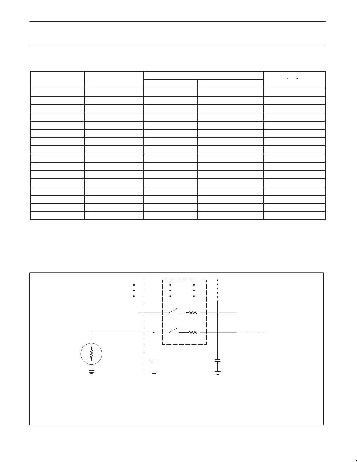
In order to obtain accurate measurements with the A/D Converter,
the source drive must be sufficient to adequately charge the
sampling capacitor during the sampling time. Figure 4 shows the
equivalent resistance and capacitance related to the A/D inputs.
accuracy (according to the A/D specifications) assuming a source
resistance of less than or equal to 20kΩ. Larger source resistances
may be accommodated by increasing the sampling time with a
different A/D timing configuration.
A/D timing configurations indicated in Table 1 allow for full A/D
AD
Sm
N+1
AD
N
+
R
S
V
ANALOG
INPUT
Sm
C
S
N+1
N
Multiplexer
Rm
Rm
N+1
N
C
C
TO COMPARATOR
Rm (multiplexer resistance) = 3 kΩ maximum
(pin capacitance) = 10 pF maximum
C
S
CC (sampling capacitor) = 2 pF maximum
RS (source resistance) = Recommended less than 20kΩ for full specified accuracy. This allows time for the sampling
capacitor (C
causes the analog input to present a varying load to the pin.
) to fully charge while the multiplexer switch is closed. Please note that sampling
C
Figure 4. A/D Input: Equivalent Circuit
SU00948
2000 Aug 22
16
Page 17
Philips Semiconductors Preliminary specification
XA 16-bit microcontroller
32 K/1 K OTP/ROM/ROMless, 8-channel 8-bit A/D, low voltage (2.7 V–5.5 V),
2
C, 2 UARTs, 16 MB address range
I
XA-S3
A/D Accuracy
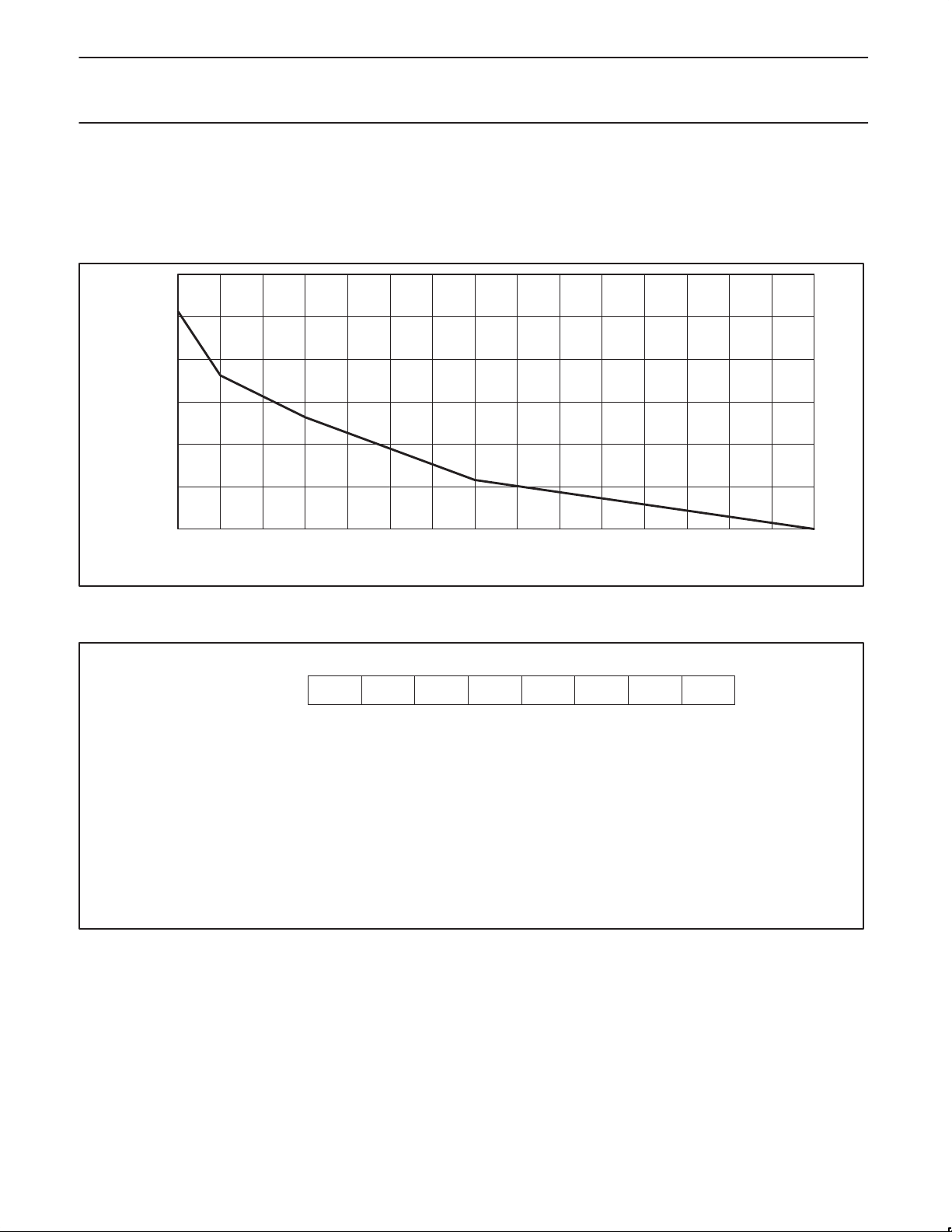
The XA-S3 A/D in 10 -bit mode is specified with 16 samples
averaged in order to factor out on-chip noise. In an application
where averaging 16 samples is not practical, the accuracy
specifications may be de-rated according to the number of samples
1.50
1.25
1.00
0.75
0.50
Additional Error (LSB)
0.25
0.00
12345678910111213141516
Number of Samples
(Pertains to 10-bit mode only. Note that 10-bit mode is only specified up to f
Figure 5. A/D accuracy by number of averaging samples
that are actually taken. The graph in Figure 5 shows the relationship
of additional A/D error to the number of samples that are averaged.
For example, if a single A/D reading is used with no averaging, the
A/D accuracy should be de-rated by ±1.25 LSB.
SU01227
= 20 MHz.)
C
I2CON Address:42Ch
Bit Addressable
Reset Value: 00h
BIT SYMBOL FUNCTION
I2CON.7 CR2 I
I2CON.6 ENA Enable I2C port. When ENA = 1, the I2C port is enabled.
I2CON.5 STA Start flag. Setting STA to 1 causes the I
I2CON.4 STO Stop flag. Setting STO to 1 causes the I2C interface to attempt to generate a Stop condition.
I2CON.3 SI Serial Interrupt. SI is set by the I2C hardware when a new I2C state is entered, indicating that
I2CON.2 AA Assert Acknowledge. Setting AA to 1 causes the I
I2CON.1 CR1 I2C Rate Control, with CR2 and CR0. See text and table.
I2CON.0 CR0 I
2
C Rate Control, with CR1 and CR0. See text and table.
2
generating a Start condition.
software needs to respond. SI causes an I
acknowledge pulses for various conditions (see text).
2
C Rate Control, with CR2 and CR1. See text and table.
Figure 6. I2C Control Register (I2CON)
C interface to attempt to gain mastership of the bus by
2
C interrupt if enabled and of sufficient priority.
2
C hardware to automatically generate
CR1AASISTOSTAENACR2
LSBMSB
CR0
SU00941
2000 Aug 22
17
Page 18

Philips Semiconductors Preliminary specification
XA 16-bit microcontroller
32 K/1 K OTP/ROM/ROMless, 8-channel 8-bit A/D, low voltage (2.7 V–5.5 V),
2
C, 2 UARTs, 16 MB address range
I
XA-S3
I2C Interface
The I2C interface on the XA-S3 is identical to the standard byte-style
2
C interface found on devices such as the 8xC552 except for the
I
rate selection.
specification, but may be used at rates up to 400 kHz
(non-conforming).
Important: Before the I2C interface may be used, the port pins
P5.6 and 5.7, which correspond to the I
respectively, must be set to the open drain mode.
The processor interfaces to the I
special function registers: I2CON (I
status register), I2DAT (I
address register). The I
bus via two port 5 pins: P5.6/SCL (serial clock line) and P5.7/SDA
(serial data line).
The Control Register, I2CON
This register is shown in Figure 6. Two bits are affected by the I
hardware: the SI bit is set when a serial interrupt is requested, and
the STO bit is cleared when a STOP condition is present on the I
bus. The STO bit is also cleared when ENA = “0”.
ENA, the I
ENA = 0: When ENA is “0”, the SDA and SCL outputs are not
driven. SDA and SCL input signals are ignored, SIO1 is in the “not
addressed” slave state, and the STO bit in I2CON is forced to “0”.
No other bits are affected. P5.6 and P5.7 may be used as open
drain I/O ports.
ENA = 1: When ENA is “1”, SIO1 is enabled. The P5.6 and P5.7
port latches must be set to logic 1.
ENA should not be used to temporarily release the I
when ENA is reset, the I
used instead (see description of the AA flag in the following text).
In the following text, it is assumed the ENA = “1”.
STA, the START flag
STA = 1: When the ST A bit is set to enter a master mode, the I
hardware checks the status of the I
condition if the bus is free. If the bus is not free, the I
waits for a STOP condition (which will free the bus) and generates a
START condition after a delay of a half clock period of the internal
serial clock generator.
If STA is set while the I
one or more bytes are transmitted or received, the hardware
transmits a repeated START condition. STA may be set at any time.
STA may also be set when the I
STA = 0: When the STA bit is reset, no START condition or
repeated START condition will be generated.
STO, the STOP flag
STO = 1: When the STO bit is set while the I
master mode, a STOP condition is transmitted to the I
the STOP condition is detected on the bus, the hardware clears the
STO flag. In a slave mode, the STO flag may be set to recover from
an error condition. In this case, no STOP condition is transmitted to
2
C bus. However, the hardware behaves as if a STOP condition
the I
has been received and switches to the defined “not addressed” slave
receiver mode. The STO flag is automatically cleared by hardware.
The I2C interface conforms to the 100 kHz I2C
2
C functions SCL and SDA
2
C logic via the following four
2
C control register), I2STA (I2C
2
C-bus since,
2
C bus and generates a STAR T
2
C interface is an addressed slave.
2
C interface
2
C interface is in a
2
2
C Enable Bit
2
C data register), and I2ADR (I2C slave
2
C control logic interfaces to the external I2C
2
C-bus status is lost. The AA flag should be
2
C interface is already in a master mode and
2
C bus. When
C
2
C
2
C
If the STA and STO bits are both set, then a STOP condition is
transmitted to the I
slave mode, the hardware generates an internal STOP condition
which is not transmitted). The I
2
C bus if the interface is in a master mode (in a
2
C interface then transmits a STAR T
condition.
STO = 0: When the STO bit is reset, no STOP condition will be
generated.
SI, the Serial Interrupt flag
SI = 1: When the SI flag is set, and the EA (interrupt system
enable) and EI2 (I
interrupt is requested. SI is set by hardware when one of 25 of the
26 possible I
2
C interrupt enable) bits are also set, an I2C
2
C interface states is entered. The only state that does
not cause SI to be set is state F8H, which indicates that no relevant
state information is available.
While SI is set, the low period of the serial clock on the SCL line is
stretched, and the serial transfer is suspended. A high level on the
SCL line is unaffected by the serial interrupt flag. SI must be reset
by software.
SI = 0: When the SI flag is reset, no serial interrupt is requested,
and there is no stretching of the serial clock on the SCL line.
AA, the Assert Acknowledge flag
AA = 1: If the AA flag is set, an acknowledge (low level to SDA) will
be returned during the acknowledge clock pulse on the SCL line when:
•The “own slave address” has been received.
•The general call address has been received while the general call
bit (GC) in I2ADR is set.
•A data byte has been received while the I
master receiver mode.
•A data byte has been received while the I
addressed slave receiver mode.
AA = 0: If the AA flag is reset, a not acknowledge (high level to
SDA) will be returned during the acknowledge clock pulse on the
SCL line when:
•A data byte has been received while the I
master receiver mode.
•A data byte has been received while the I
addressed slave receiver mode.
When the I2C interface is in the addressed slave transmitter mode,
state C8H will be entered after the last serial data byte is
transmitted. When SI is cleared, the I
enters the not addressed slave receiver mode, and the SDA line
remains at a high level. In state C8H, the AA flag can be set again
for future address recognition.
When the I
slave address and the general call address are ignored. Consequently,
no acknowledge is returned, and a serial interrupt is not requested.
Thus, the hardware can be temporarily released from the I
while the bus status is monitored. While the hardware is released from
the bus, START and STOP conditions are detected, and serial data is
shifted in. Address recognition can be resumed at any time by setting
the AA flag. If the AA flag is set when the part’s own slave address or
the general call address has been partly received, the address will be
recognized at the end of the byte transmission.
2
C interface is in the not addressed slave mode, its own
2
C interface is in the
2
C interface is in the
2
C interface is in the
2
C interface is in the
2
C interface leaves state C8H,
2
C bus
2000 Aug 22
18
Page 19
Philips Semiconductors Preliminary specification
qy
Clock Divisor
XA 16-bit microcontroller
32 K/1 K OTP/ROM/ROMless, 8-channel 8-bit A/D, low voltage (2.7 V–5.5 V),
2
C, 2 UARTs, 16 MB address range
I
XA-S3
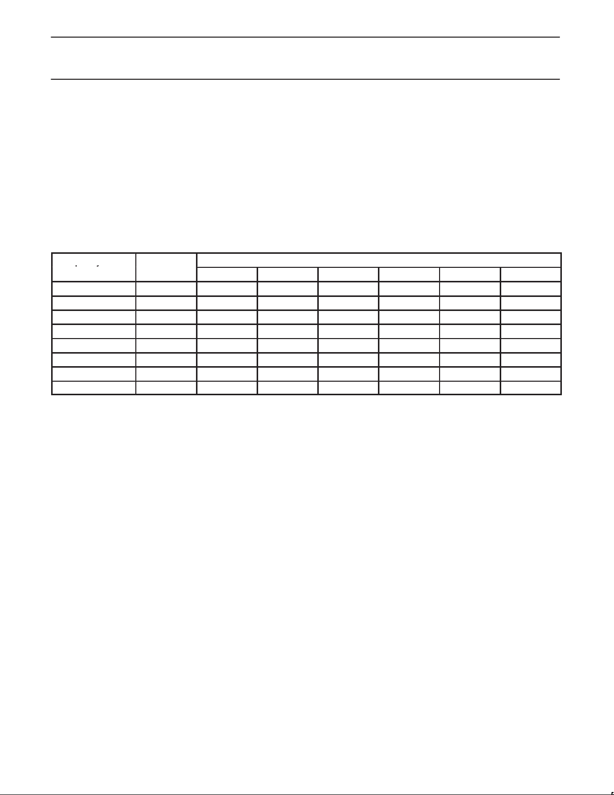
CR0, CR1, and CR2, the Clock Rate Bits
These three bits determine the serial clock frequency when the I
interface is in a master mode. An I
2
C rate of 100kHz or lower is
2
C
typical and can be derived from many oscillator frequencies. The
various serial rates are shown in Table 4. A variable bit rate may
also be used if Timer 1 is not required for any other purpose while
2
the I
C hardware is in a master mode. The frequencies shown in
Table 4 are unimportant when the I
2
C hardware is in a slave mode.
In the slave modes, the hardware will automatically synchronize with
the incoming clock frequency.
The I2C Status Register, I2STA
I2STA is an 8-bit read-only special function register. The three least
significant bits are always zero. The five most significant bits contain
the status code. There are 26 possible status codes. When I2STA
contains F8H, no relevant state information is available and no serial
interrupt is requested. All other I2STA values correspond to defined
hardware interface states. When each of these states is entered, a
serial interrupt is requested (SI = “1”).
NOTE: A detailed I
information, including example driver code, will be provided in
2
C interface description and usage
a separate document.
Table 4. I2C Rate Control
Frequency Select
(CR2, CR1, CR0)
0h (0000) 20 (400)
1h (0001) 40 (200)
2h (0010) 68 (116.65)
8 MHz 12 MHz 16 MHz 20 MHz 24 MHz 30 MHz
1
1
1
3h (0011) 88 90.91 (136.36)
4h (0100) 160 50 75 100 (125)
5h (0101) 272 29.41 44.12 58.82 73.53 88.24 (110.29)
6h (0110) 352 22.73 34.09 45.45 56.82 68.18 85.23
7h (0111) (Timer 1)
NOTES:
1. The XA-S3 I
2
C interface does not conform to the 400kHz I2C specification (which applies to rates greater than 100kHz) in all details, but
may be used with care where higher rates are required by the application.
2. The timer 1 overflow is used to clock the I
2
(Timer 1)
2
2
C interface. The resulting bit rate is 1/2 of the timer overflow rate.
Example I2C Rates at Specific Oscillator Frequencies
– – – – –
(300)
(176.46)
(Timer 1)
1
1
1
2
(400)
(235.29)
(181.82)
(Timer 1)
1
1
1
2
– – –
(294.12)
(227.27)
(Timer 1)
1
1
1
2
(Timer 1)
(352.94)
(272.73)
(150)
1
1
1
2
(340.91)
(187.5)
(Timer 1)
–
1
1
1
2
2000 Aug 22
19
Page 20
Philips Semiconductors Preliminary specification
XA 16-bit microcontroller
32 K/1 K OTP/ROM/ROMless, 8-channel 8-bit A/D, low voltage (2.7 V–5.5 V),
2
C, 2 UARTs, 16 MB address range
I
XA-S3
XA-S3 Timer/Counters
The XA-S3 has three general purpose counter/timers, two of which may
also be used as baud rate generators for either or both of the UARTs.
Timer 0 and 1
These are identical to the standard XA-G3 timer 0 and 1.
Timer 2
This is identical to the standard XA-G3 timer 2.
Programmable Counter Array (PCA)
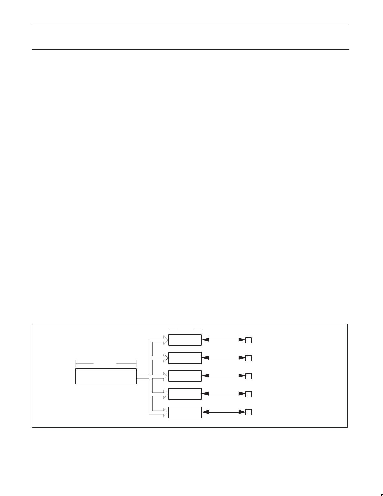
The Programmable Counter Array available on the XA-S3 is a
special 16-bit Timer that has five 16-bit capture/compare modules
associated with it. Each of the modules can be programmed to
operate in one of four modes: rising and/or falling edge capture,
software timer, high-speed output, or pulse width modulator. Each
module has a pin associated with it in port 1. Module 0 is connected
to P4.1(CEX0), module 1 to P4.2(CEX1), etc. The basic PCA
configuration is shown in Figure 7.
The PCA timer is a common time base for all five modules and can
be programmed to run at: the TCLK rate (Osc/4, Osc/16, or Osc/64),
the Timer 0 overflow , or the input on the ECI pin (P4.0). When the
ECI input is used, the falling edge clocks the PCA counter. The timer
count source is determined from the CPS1 and CPS0 bits in the
CMOD SFR as follows (see Figure 10):
CPS1 CPS0 PCA Timer Count Source
0 X TCLK (Osc/4, Osc/16, or Osc/64)
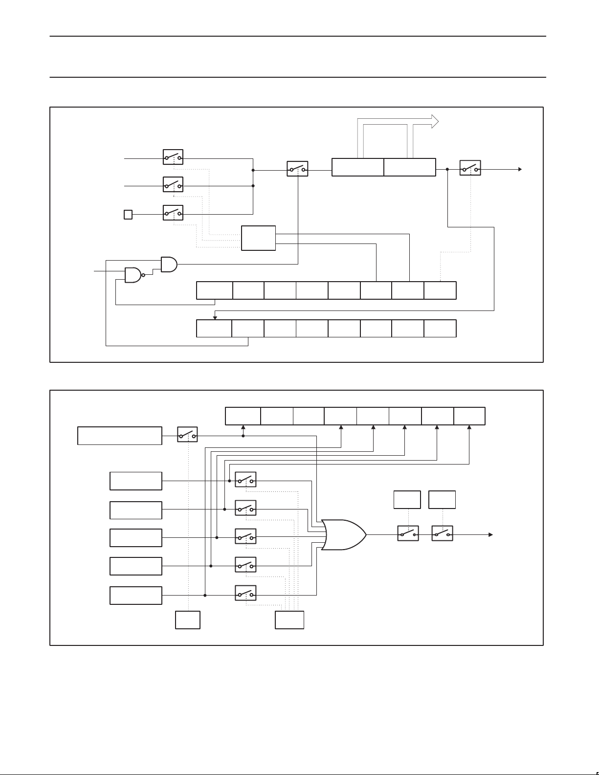
1 0 Timer 0 overflow
1 1 ECI (PCA External Clock Input (max rate = Osc/4)
In the CMOD SFR are three additional bits associated with the PCA.
They are CIDL which allows the PCA to stop during idle mode,
WDTE which enables or disables the watchdog function on
module 4, and ECF which when set causes an interrupt and the
PCA overflow flag CF (in the CCON SFR) to be set when the PCA
timer overflows. These functions are shown in Figure 8. In addition,
each PCA module may generate a separate interrupt.
The watchdog timer function is implemented in module 4 (see
Figure 17).
The CCON SFR contains the run control bit for the PCA and the
flags for the PCA timer (CF) and each module (refer to Figure 11).
To run the PCA the CR bit (CCON.6) must be set by software. The
PCA is shut off by clearing this bit. The CF bit (CCON.7) is set when
the PCA counter overflows and an interrupt will be generated if the
ECF bit in the CMOD register is set, The CF bit can only be cleared
by software. Bits 0 through 4 of the CCON register are the flags for
the modules (bit 0 for module 0, bit 1 for module 1, etc.) and are set
by hardware when either a match or a capture occurs. These flags
also can only be cleared by software. The PCA interrupt system
shown in Figure 9.
Each module in the PCA has a special function register associated
with it. These registers are: CCAPM0 for module 0, CCAPM1 for
module 1, etc. (see Figure 12). The registers contain the bits that
control the mode that each module will operate in. The ECCF bit
(CCAPMn.0 where n=0, 1, 2, 3, or 4 depending on the module)
enables the CCF flag in the CCON SFR to generate an interrupt
when a match or compare occurs in the associated module. PWM
(CCAPMn.1) enables the pulse width modulation mode. The TOG
bit (CCAPMn.2) when set causes the CEX output associated with
the module to toggle when there is a match between the PCA
counter and the module’s capture/compare register. The match bit
MAT (CCAPMn.3) when set will cause the CCFn bit in the CCON
register to be set when there is a match between the PCA counter
and the module’s capture/compare register.
The next two bits CAPN (CCAPMn.4) and CAPP (CCAPMn.5)
determine the edge that a capture input will be active on. The CAPN
bit enables the negative edge, and the CAPP bit enables the
positive edge. If both bits are set both edges will be enabled and a
capture will occur for either transition. The last bit in the register
ECOM (CCAPMn.6) when set enables the comparator function.
Figure 13 shows the CCAPMn settings for the various PCA
functions.
There are two additional registers associated with each of the PCA
modules. They are CCAPnH and CCAPnL and these are the
registers that store the 16-bit count when a capture occurs or a
compare should occur. When a module is used in the PWM mode
these registers are used to control the duty cycle of the output.
MODULE FUNCTIONS:
16-BIT CAPTURE
16-BIT TIMER
16-BIT HIGH SPEED OUTPUT
8-BIT PWM
WATCHDOG TIMER (MODULE 4 ONLY)
2000 Aug 22
16 BITS
PCA TIMER/COUNTER
TIME BASE FOR PCA MODULES
16 BITS
MODULE 0
MODULE 1
MODULE 2
MODULE 3
MODULE 4
Figure 7. Programmable Counter Array (PCA)
20
P4.1/CEX0
P4.2/CEX1
P4.3/CEX2
P4.4/CEX3
P4.5/CEX4
SU01303
Page 21
Philips Semiconductors Preliminary specification
XA 16-bit microcontroller
32 K/1 K OTP/ROM/ROMless, 8-channel 8-bit A/D, low voltage (2.7 V–5.5 V),
2
C, 2 UARTs, 16 MB address range
I
TO PCA
MODULES
XA-S3
TCLK
(OSC/4, OSC/16,
OR OSC/64)
TIMER 0
OVERFLOW
EXTERNAL INPUT
(P4.0/ECI)
IDLE
OVERFLOW
CH CL
16–BIT UP COUNTER
01
DECODE
10
11
CIDL WDTE –– –– –– CPS1 CPS0 ECF
CF CR CCF4 CCF3 CCF2 CCF1 CCF0––
Figure 8. PCA Timer/Counter
CF CR CCF4 CCF3 CCF2 CCF1 CCF0––
CMOD
(490H)
CCON
(41AH)
INTERRUPT
SU01304
CCON
(41AH)
PCA TIMER/COUNTER
MODULE 0
MODULE 1
MODULE 2
MODULE 3
MODULE 4
CMOD.0 ECF
CCAPMn.0 ECCFn
Figure 9. PCA Interrupt System
IEL.5
EPC
IEL.7
EA
TO
INTERRUPT
PRIORITY
DECODER
SU01305
2000 Aug 22
21
Page 22
Philips Semiconductors Preliminary specification
XA 16-bit microcontroller
32 K/1 K OTP/ROM/ROMless, 8-channel 8-bit A/D, low voltage (2.7 V–5.5 V),
2
C, 2 UARTs, 16 MB address range
I
XA-S3
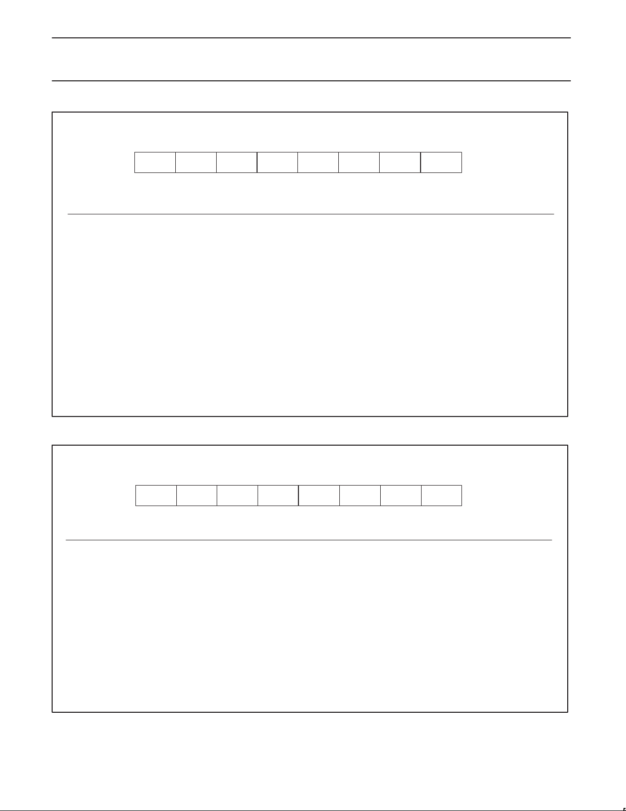
CMOD Address = 490H
Reset Value = 00H
CIDL WDTE – – – CPS1 CPS0 ECF
Bit:
76543210
Symbol Function
CIDL Counter Idle control: CIDL = 0 programs the PCA Counter to continue functioning during idle Mode. CIDL = 1 programs
it to be gated off during idle.
WDTE Watchdog Timer Enable: WDTE = 0 disables Watchdog Timer function on PCA Module 4. WDTE = 1 enables it.
– Not implemented, reserved for future use.*
CPS1 PCA Count Pulse Select bit 1.
CPS0 PCA Count Pulse Select bit 0.
CPS1 CPS0 PCA Timer Count Source
0 X TClk (Osc/4, Osc/16, or Osc/64)
1 0 Timer 0 overflow
1 1 ECI (PCA External Clock Input (max rate = Osc/4)
ECF PCA Enable Counter Overflow interrupt: ECF = 1 enables CF bit in CCON to generate an interrupt. ECF = 0 disables
that function of CF.
NOTE:
* User software should not write 1s to reserved bits. These bits may be used in future products to invoke new features. In that case, the reset or inactive value of the new bit will be
0, and its active value will be 1. The value read from a reserved bit is indeterminate.
** f
= oscillator frequency
OSC
SU01306
Figure 10. CMOD: PCA Counter Mode Register
CCON Address = 41AH
Reset Value = 00H
Bit Addressable
CF CR – CCF4 CCF3 CCF2 CCF1 CCF0
Bit:
76543210
Symbol Function
CF PCA Counter Overflow flag. Set by hardware when the counter rolls over. CF flags an interrupt if bit ECF in CMOD is
set. CF may be set by either hardware or software but can only be cleared by software.
CR PCA Counter Run control bit. Set by software to turn the PCA counter on. Must be cleared by software to turn the PCA
counter off.
– Not implemented, reserved for future use*.
CCF4 PCA Module 4 interrupt flag. Set by hardware when a match or capture occurs. Must be cleared by software.
CCF3 PCA Module 3 interrupt flag. Set by hardware when a match or capture occurs. Must be cleared by software.
CCF2 PCA Module 2 interrupt flag. Set by hardware when a match or capture occurs. Must be cleared by software.
CCF1 PCA Module 1 interrupt flag. Set by hardware when a match or capture occurs. Must be cleared by software.
CCF0 PCA Module 0 interrupt flag. Set by hardware when a match or capture occurs. Must be cleared by software.
Each of CCF4 through CCF0 generates its own interrupt, and has its own interrupt vector.
NOTE:
* User software should not write 1s to reserved bits. These bits may be used in future products to invoke new features. In that case, the reset or inactive value of the new bit will be
0, and its active value will be 1. The value read from a reserved bit is indeterminate.
SU01307
Figure 11. CCON: PCA Counter Control Register
2000 Aug 22
22
Page 23
Philips Semiconductors Preliminary specification
XA 16-bit microcontroller
32 K/1 K OTP/ROM/ROMless, 8-channel 8-bit A/D, low voltage (2.7 V–5.5 V),
2
C, 2 UARTs, 16 MB address range
I
XA-S3
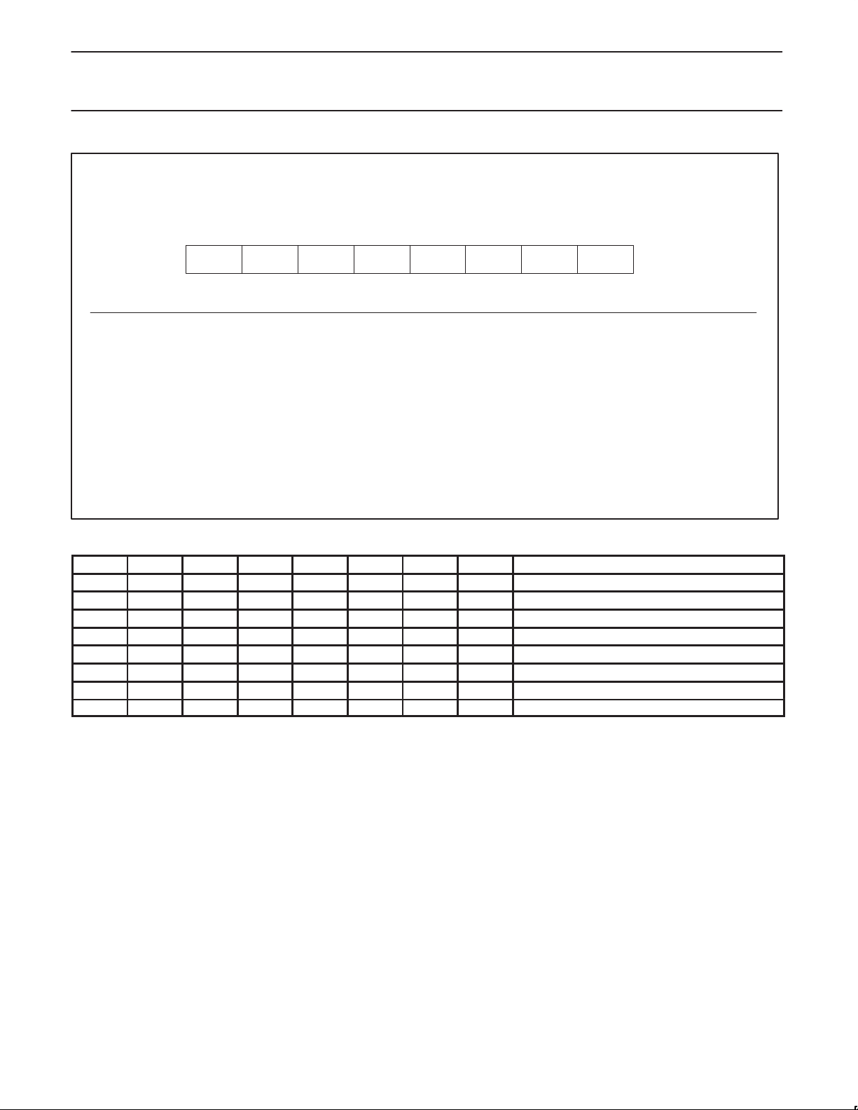
CCAPMn Address CCAPM0 491H
Not Bit Addressable
Bit:
Symbol Function
– Not implemented, reserved for future use*.
ECOMn Enable Comparator. ECOMn = 1 enables the comparator function.
CAPPn Capture Positive, CAPPn = 1 enables positive edge capture.
CAPNn Capture Negative, CAPNn = 1 enables negative edge capture.
MATn Match. When MATn = 1, a match of the PCA counter with this module’s compare/capture register causes the CCFn bit
TOGn Toggle. When TOGn = 1, a match of the PCA counter with this module’s compare/capture register causes the CEXn
PWMn Pulse Width Modulation Mode. PWMn = 1 enables the CEXn pin to be used as a pulse width modulated output.
ECCFn Enable CCF interrupt. Enables compare/capture flag CCFn in the CCON register to generate an interrupt.
NOTE:
*User software should not write 1s to reserved bits. These bits may be used in future products to invoke new features. In that case, the reset or inactive value of the new bit will be 0,
and its active value will be 1. The value read from a reserved bit is indeterminate.
–
X 0 0 0 0 0 0 0 No operation
X X 1 0 0 0 0 X 16-bit capture by a positive-edge trigger on CEXn
X X 0 1 0 0 0 X 16-bit capture by a negative trigger on CEXn
X X 1 1 0 0 0 X 16-bit capture by a transition on CEXn
X 1 0 0 1 0 0 X 16-bit Software Timer
X 1 0 0 1 1 0 X 16-bit High Speed Output
X 1 0 0 0 0 1 0 8-bit PWM
X 1 0 0 1 X 0 X Watchdog Timer
in CCON to be set, flagging an interrupt.
pin to toggle.
ECOMn CAPPn CAPNn MATn TOGn PWMn ECCFn MODULE FUNCTION
CCAPM1 492H
CCAPM2 493H
CCAPM3 494H
CCAPM4 495H
– ECOMn CAPPn CAPNn MATn TOGn PWMn ECCFn
76543210
Figure 12. CCAPMn: PCA Modules Compare/Capture Registers
Figure 13. PCA Module Modes (CCAPMn Register)
Reset Value = 00H
SU01308
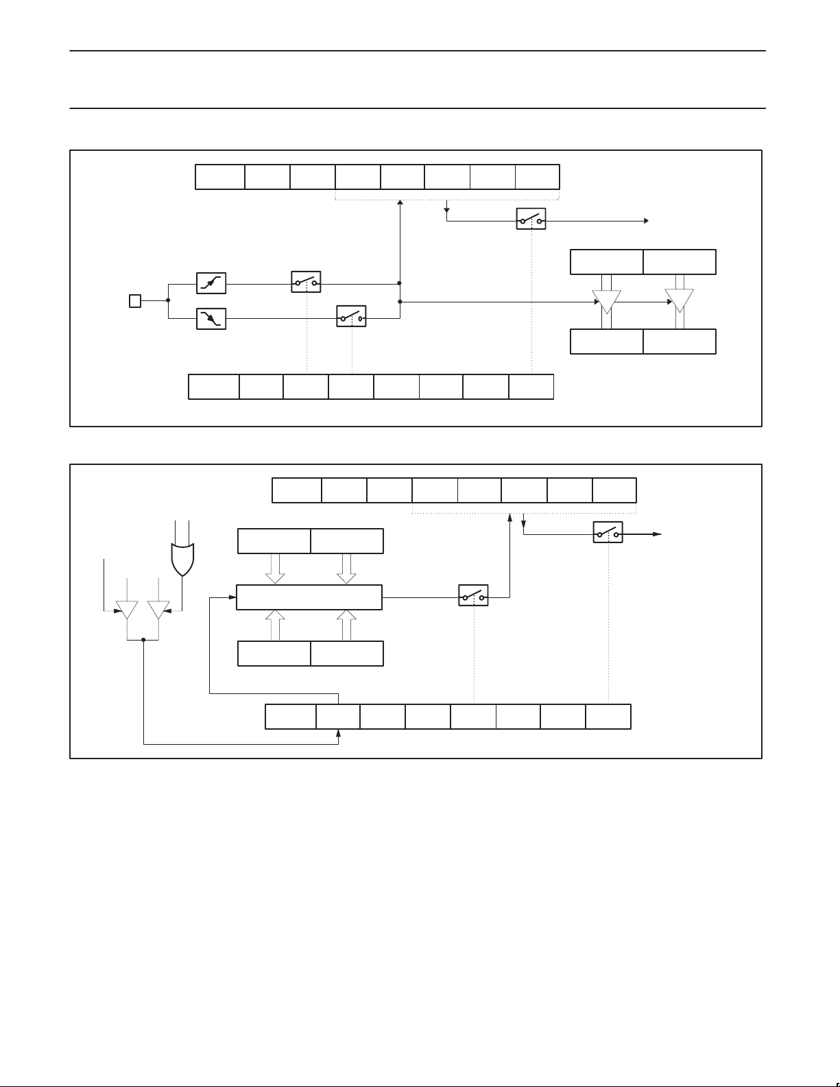
PCA Capture Mode
To use one of the PCA modules in the capture mode either one or
both of the CCAPM bits CAPN and CAPP for that module must be
set. The external CEX input for the module (on port 1) is sampled for
a transition. When a valid transition occurs the PCA hardware loads
the value of the PCA counter registers (CH and CL) into the
module’s capture registers (CCAPnL and CCAPnH). If the CCFn bit
for the module in the CCON SFR and the ECCFn bit in the CCAPMn
SFR are set then an interrupt will be generated. Refer to Figure 14.
16-bit Software Timer Mode
The PCA modules can be used as software timers by setting both
the ECOM and MAT bits in the modules CCAPMn register. The PCA
timer will be compared to the module’s capture registers and when a
match occurs an interrupt will occur if the CCFn (CCON SFR) and
the ECCFn (CCAPMn SFR) bits for the module are both set (see
Figure 15).
High Speed Output Mode
In this mode the CEX output (on port 4) associated with the PCA
module will toggle each time a match occurs between the PCA
2000 Aug 22
counter and the module’s capture registers. To activate this mode
the TOG, MAT, and ECOM bits in the module’s CCAPMn SFR must
be set (see Figure 16).
Pulse Width Modulator Mode
All of the PCA modules can be used as PWM outputs. Figure 17
shows the PWM function. The frequency of the output depends on
the source for the PCA timer. All of the modules will have the same
frequency of output because they all share the PCA timer. The duty
cycle of each module is independently variable using the module’s
capture register CCAPLn. When the value of the PCA CL SFR is
less than the value in the module’s CCAPLn SFR the output will be
low, when it is equal to or greater than the output will be high. When
CL overflows from FF to 00, CCAPLn is reloaded with the value in
CCAPHn. the allows updating the PWM without glitches. The PWM
and ECOM bits in the module’s CCAPMn register must be set to
enable the PWM mode.
23
Page 24
Philips Semiconductors Preliminary specification
XA 16-bit microcontroller
32 K/1 K OTP/ROM/ROMless, 8-channel 8-bit A/D, low voltage (2.7 V–5.5 V),
2
C, 2 UARTs, 16 MB address range
I
XA-S3
CEXn
WRITE TO
CCAPnL
WRITE TO
CCAPnH
01
CF CR CCF4 CCF3 CCF2 CCF1 CCF0––
(TO CCFn)
CAPTURE
–– ECOMn CAPPn CAPNn MATn TOGn PWMn ECCFn
0 000
Figure 14. PCA Capture Mode
CF CR CCF4 CCF3 CCF2 CCF1 CCF0––
RESET
CCAPnL
(TO CCFn)
MATCH
ENABLE
CCAPnH
16–BIT COMPARATOR
CCON
(41AH)
PCA TIMER/COUNTER
CH CL
CCAPnH CCAPnL
CCAPMn, n= 0 to 4
(491H–495H)
PCA INTERRUPT
SU01309
CCON
(41AH)
PCA INTERRUPT
CH CL
PCA TIMER/COUNTER
–– ECOMn CAPPn CAPNn MATn TOGn PWMn ECCFn
0000
Figure 15. PCA Compare Mode
CCAPMn, n= 0 to 4
(491H–495H)
SU01310
2000 Aug 22
24
Page 25
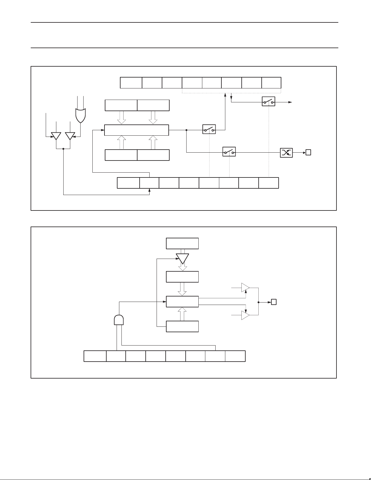
Philips Semiconductors Preliminary specification
XA 16-bit microcontroller
32 K/1 K OTP/ROM/ROMless, 8-channel 8-bit A/D, low voltage (2.7 V–5.5 V),
2
C, 2 UARTs, 16 MB address range
I
XA-S3
WRITE TO
CCAPnL
WRITE TO
CCAPnH
01
RESET
ENABLE
CF CR CCF4 CCF3 CCF2 CCF1 CCF0––
CCAPnH CCAPnL
16–BIT COMPARATOR
CH CL
PCA TIMER/COUNTER
–– ECOMn CAPPn CAPNn MATn TOGn PWMn ECCFn
MATCH
(TO CCFn)
1000
Figure 16. PCA High Speed Output Mode
CCAPnH
CCON
(41AH)
TOGGLE
CCAPMn, n: 0..4
(491H–495H)
PCA INTERRUPT
CEXn
SU01311
CCAPnL
0
ENABLE
OVERFLOW
–– ECOMn CAPPn CAPNn MATn TOGn PWMn ECCFn
8–BIT
COMPARATOR
CL
PCA TIMER/COUNTER
0
CL < CCAPnL
CL >= CCAPnL
1
0000
Figure 17. PCA PWM Mode
CCAPMn, n: 0..4
(491H–495H)
SU01312
CEXn
2000 Aug 22
25
Page 26
Philips Semiconductors Preliminary specification
XA 16-bit microcontroller
32 K/1 K OTP/ROM/ROMless, 8-channel 8-bit A/D, low voltage (2.7 V–5.5 V),
2
C, 2 UARTs, 16 MB address range
I
XA-S3
CIDL WDTE –– –– –– CPS1 CPS0 ECF
WRITE TO
CCAP4L
WRITE TO
CCAP4H
01
RESET
ENABLE
CCAP4H CCAP4L
16–BIT COMPARATOR
CH CL
PCA TIMER/COUNTER
–– ECOMn CAPPn CAPNn MA Tn TOGn PWMn ECCFn
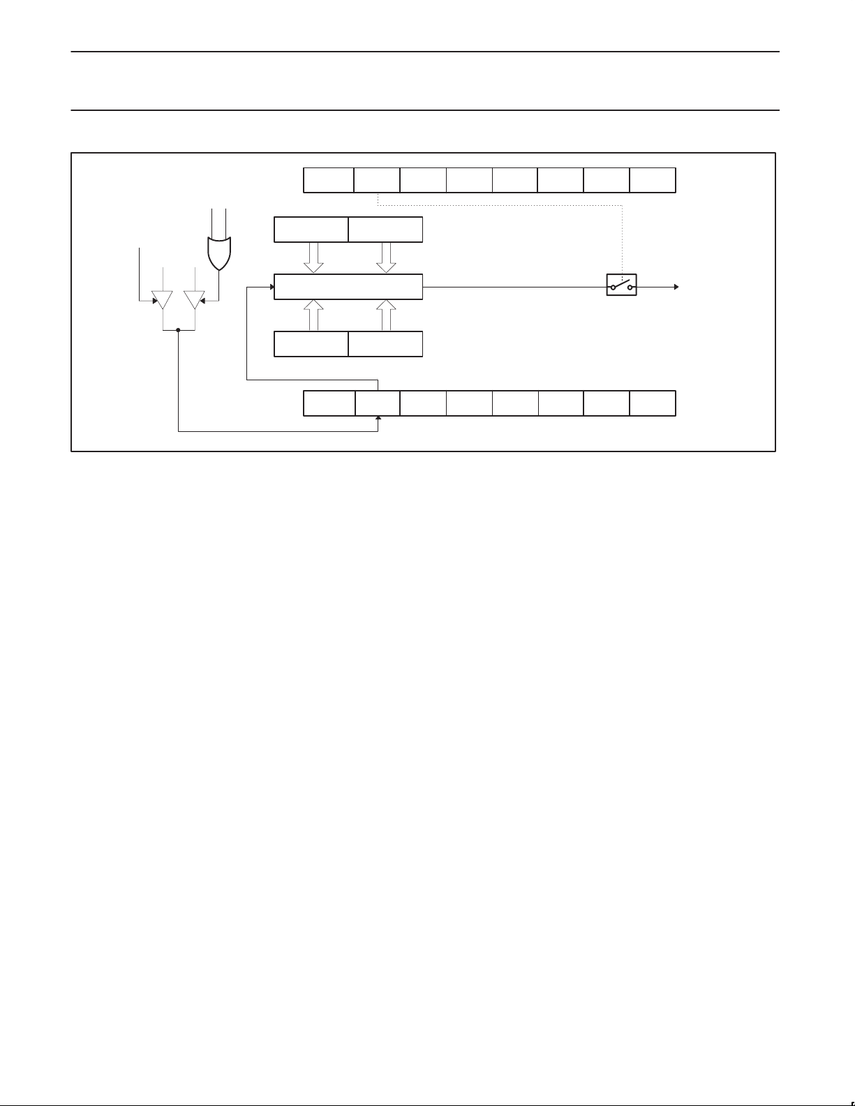
Figure 18. PCA Watchdog Timer m(Module 4 only)
PCA Watchdog Timer
An on-board watchdog timer is available with the PCA to improve
the reliability of the system without increasing chip count. Watchdog
timers are useful for systems that are susceptible to noise, power
glitches, or electrostatic discharge. Module 4 is the only PCA
module that can be programmed as a watchdog. However, this
module can still be used for other modes if the watchdog is not
needed.
Figure 18 shows a diagram of how the watchdog works. The user
pre-loads a 16-bit value in the compare registers. Just like the other
compare modes, this 16-bit value is compared to the PCA timer
value. If a match is allowed to occur, an internal reset will be
generated. This will not cause the RST pin to be driven low.
In order to hold off the reset, the user has three options:
1. periodically change the compare value so it will never match the
PCA timer,
2. periodically change the PCA timer value so it will never match
the compare values, or
3. disable the watchdog by clearing the WDTE bit before a match
occurs and then re-enable it.
CMOD
(490H)
MODULE 4
MATCH
1
X000
RESET
CCAPM4
(495H)
X
SU01313
The first two options are more reliable because the watchdog timer
is never disabled as in option #3. If the program counter ever goes
astray, a match will eventually occur and cause an internal reset.
The second option is also not recommended if other PCA modules
are being used. Remember , the PCA timer is the time base for all
modules; changing the time base for other modules would not be a
good idea. Thus, in most applications the first solution is the best
option.
Figure 19 shows the code for initializing the watchdog timer. Module
4 can be configured in either compare mode, and the WDTE bit in
CMOD must also be set. The user’s software then must periodically
change (CCAP4H,CCAP4L) to keep a match from occurring with the
PCA timer (CH,CL). This code is given in the WATCHDOG routine in
Figure 19.
This routine should not be part of an interrupt service routine,
because if the program counter goes astray and gets stuck in an
infinite loop, interrupts will still be serviced and the watchdog will
keep getting reset. Thus, the purpose of the watchdog would be
defeated. Instead, call this subroutine from the main program within
16
2
count of the PCA timer.
2000 Aug 22
26
Page 27

Philips Semiconductors Preliminary specification
XA 16-bit microcontroller
32 K/1 K OTP/ROM/ROMless, 8-channel 8-bit A/D, low voltage (2.7 V–5.5 V),
2
C, 2 UARTs, 16 MB address range
I
INIT_WATCHDOG:
MOV CCAPM4, #4CH ; Module 4 in compare mode
MOV CCAP4L, #0FFH ; Write to low byte first
MOV CCAP4H, #0FFH ; Before PCA timer counts up to
; FFFF Hex, these compare values
; must be changed
OR CMOD, #40H ; Set the WDTE bit to enable the
; watchdog timer without changing
; the other bits in CMOD
;
;********************************************************************
;
; Main program goes here, but CALL WATCHDOG periodically.
;
;********************************************************************
;
WATCHDOG:
CLR EA ; Hold off interrupts
MOV CCAP4L, #00 ; Next compare value is within
MOV CCAP4H, CH ; 255 counts of the current PCA
SETB EA ; timer value
RET
XA-S3
Figure 19. PCA Watchdog Timer Initialization Code
Watchdog Timer
This is a standard XA-G3 watchdog timer. This watchdog timer
always comes up running at reset. The watchdog acts the same on
EPROM, ROM, and ROMless parts, as in the XA-G3.
UARTs
Standard XA-S3 UART0 and UART1 with double buffered transmit
register. A flag has been added to SnSTAT that is set if any of the
status flags (BRn, FEn, or OEn) is set for the corresponding UART
channel. This allows polling for UART errors quickly at the interrupt
service routine. Baud rate sources may be timer 1 or timer 2.
The XA-S3 includes 2 UART ports that are compatible with the
enhanced UART used on the XA-G3.
The UART has separate interrupt vectors for each UART’s transmit
and receive functions. The UART transmitter has been double
buffered, allowing packed transmission of data with no gaps
between bytes and less critical interrupt service routine timing. A
break detect function has been added to the UART. This operates
independently of the UART itself and provides a start-of-break
status bit that the program may test. An Overrun Error flag allows
detection of missed characters in the received data stream. The
double buffered UART transmitter may require some software
changes if code is used that was written for the original XA-G3
single buffered UART.
Each UART baud rate is determined by either a fixed division of the
oscillator (in UART modes 0 and 2) or by the timer 1 or timer 2
overflow rate (in UART modes 1 and 3).
Timer 1 defaults to clock both UART0 and UART1. Timer 2 can be
programmed to clock either UART0 through T2CON (via bits R0CLK
and T0CLK) or UART1 through T2MOD (via bits R1CLK and
T1CLK). In this case, the UART not clocked by T2 could use T1 as
the clock source.
The serial port receive and transmit registers are both accessed at
Special Function Register SnBUF. Writing to SnBUF loads the
transmit register, and reading SnBUF accesses a physically
separate receive register.
The serial port can operate in 4 modes:
Mode 0: Serial I/O expansion mode. Serial data enters and exits
through RxDn. TxDn outputs the shift clock. 8 bits are
transmitted/received (LSB first). (The baud rate is fixed at 1/16 the
oscillator frequency.)
Mode 1: Standard 8-bit UART mode. 10 bits are transmitted
(through TxDn) or received (through RxDn): a start bit (0), 8 data
bits (LSB first), and a stop bit (1). On receive, the stop bit goes into
RB8 in Special Function Register SnCON. The baud rate is variable.
Mode 2: Fixed rate 9-bit UART mode. 11 bits are transmitted
(through TxD) or received (through RxD): start bit (0), 8 data bits
(LSB first), a programmable 9th data bit, and a stop bit (1). On
Transmit, the 9th data bit (TB8_n in SnCON) can be assigned the
value of 0 or 1. Or, for example, the parity bit (P, in the PSW) could
be moved into TB8_n. On receive, the 9th data bit goes into RB8_n
in Special Function Register SnCON, while the stop bit is ignored.
The baud rate is programmable to 1/32 of the oscillator frequency.
Mode 3: Standard 9-bit UART mode. 11 bits are transmitted
(through TxDn) or received (through RxDn): a start bit (0), 8 data
bits (LSB first), a programmable 9th data bit, and a stop bit (1).
In fact, Mode 3 is the same as Mode 2 in all respects except baud
rate. The baud rate in Mode 3 is variable.
In all four modes, transmission is initiated by any instruction that
uses SnBUF as a destination register. Reception is initiated in
Mode 0 by the condition RI_n = 0 and REN_n = 1. Reception is
initiated in the other modes by the incoming start bit if REN_n = 1.
2000 Aug 22
27
Page 28
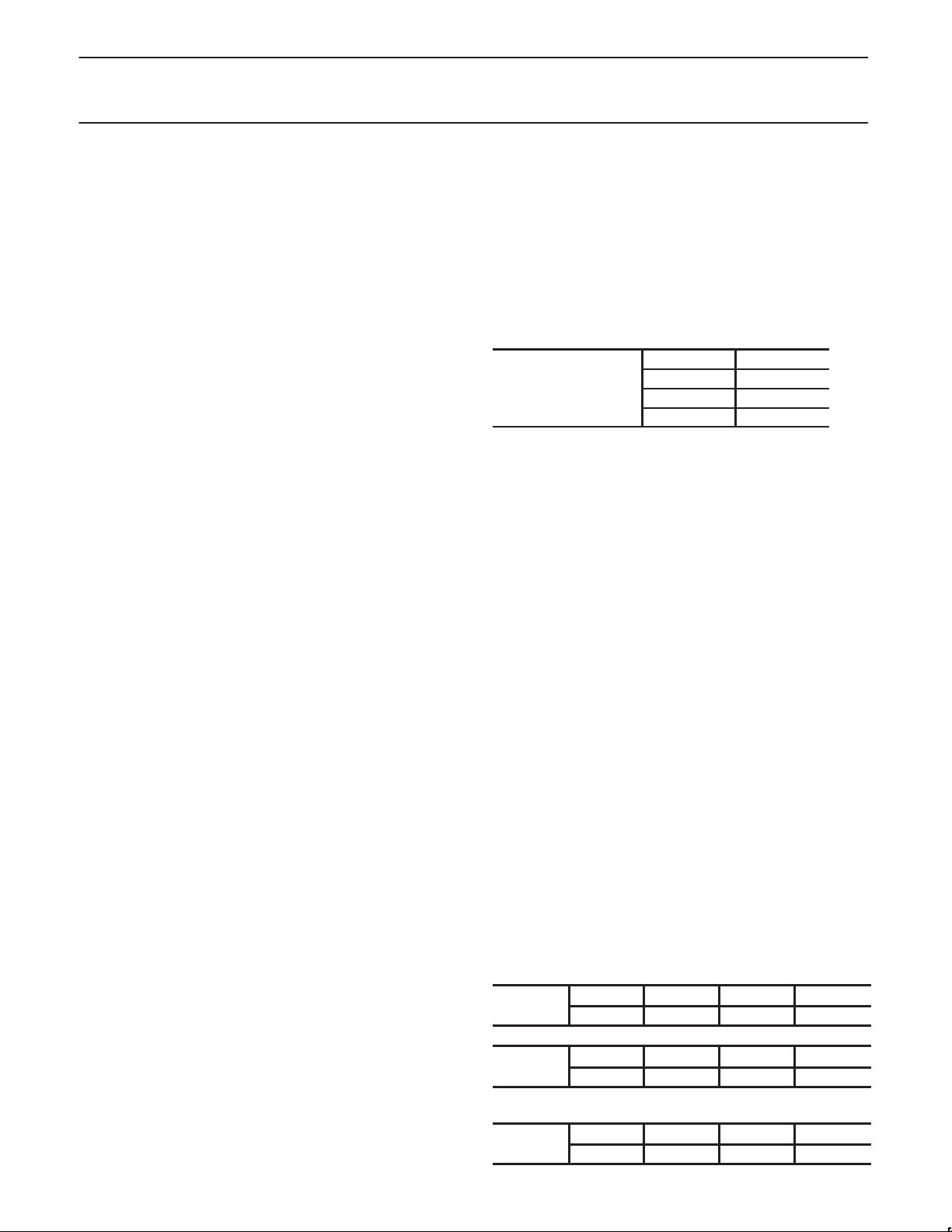
Philips Semiconductors Preliminary specification
f
2
controlled by PT1, PT0
XA 16-bit microcontroller
32 K/1 K OTP/ROM/ROMless, 8-channel 8-bit A/D, low voltage (2.7 V–5.5 V),
2
C, 2 UARTs, 16 MB address range
I
XA-S3
Serial Port Control Register
The serial port control and status register is the Special Function
Register SnCON, shown in Figure 21. This register contains not only
the mode selection bits, but also the 9th data bit for transmit and
receive (TB8_n and RB8_n), and the serial port interrupt bits (TI_n
and RI_n).
TI Flag
In order to allow easy use of the double buffered UART transmitter
feature, the TI_n flag is set by the UART hardware under two
conditions. The first condition is the completion of any byte
transmission. This occurs at the end of the stop bit in modes 1, 2, or
3, or at the end of the eighth data bit in mode 0. The second
condition is when SnBUF is written while the UART transmitter is
idle. In this case, the TI_n flag is set in order to indicate that the
second UART transmitter buffer is still available.
Typically, UART transmitters generate one interrupt per byte
transmitted. In the case of the XA UART, one additional interrupt is
generated as defined by the stated conditions for setting the TI_n
flag. This additional interrupt does not occur if double buffering is
bypassed as explained below. Note that if a character oriented
approach is used to transmit data through the UART, there could be
a second interrupt for each character transmitted, depending on the
timing of the writes to SBUF. For this reason, it is generally better to
bypass double buffering when the UART transmitter is used in
character oriented mode. This is also true if the UART is polled
rather than interrupt driven, and when transmission is character
oriented rather than message or string oriented. The interrupt occurs
at the end of the last byte transmitted when the UART becomes idle.
Among other things, this allows a program to determine when a
message has been transmitted completely. The interrupt service
routine should handle this additional interrupt.
The recommended method of using the double buffering in the
application program is to have the interrupt service routine handle a
single byte for each interrupt occurrence. In this manner the program
essentially does not require any special considerations for double
buffering. Unless higher priority interrupts cause delays in the servicing
of the UART transmitter interrupt, the double buffering will result in
transmitted bytes being tightly packed with no intervening gaps.
9-bit Mode
Please note that the ninth data bit (TB8) is not double buffered. Care
must be taken to insure that the TB8 bit contains the intended data
at the point where it is transmitted. Double buffering of the UART
transmitter may be bypassed as a simple means of synchronizing
TB8 to the rest of the data stream.
Bypassing Double Buffering
The UART transmitter may be used as if it is single buffered. The
recommended UART transmitter interrupt service routine (ISR)
technique to bypass double buffering first clears the TI_n flag upon
entry into the ISR, as in standard practice. This clears the interrupt
that activated the ISR. Secondly, the TI_n flag is cleared immediately
following each write to SnBUF. This clears the interrupt flag that would
otherwise direct the program to write to the second transmitter buffer.
If there is any possibility that a higher priority interrupt might become
active between the write to SnBUF and the clearing of the TI_n flag,
the interrupt system may have to be temporarily disabled during that
sequence by clearing, then setting the EA bit in the IEL register.
CLOCKING SCHEME/BAUD RATE GENERATION
The XA UARTS clock rates are determined by either a fixed division
(modes 0 and 2) of the oscillator clock or by the Timer 1 or Timer 2
overflow rate (modes 1 and 3).
The clock for the UARTs in XA runs at 16x the Baud rate. If the
timers are used as the source for Baud Clock, since maximum
speed of timers/Baud Clock is Osc/4, the maximum baud rate is
timer overflow divided by 16 i.e. Osc/64.
In Mode 0, it is fixed at Osc/16. In Mode 2, however, the fixed rate
is Osc/32.
00 Osc/4
Pre-scaler
or all Timers T0,1,
controlled by PT1, PT0
bits in SCR
Baud Rate for UART Mode 0:
Baud_Rate = Osc/16
Baud Rate calculation for UART Mode 1 and 3:
Baud_Rate = Timer_Rate/16
Timer_Rate = Osc/(N*(Timer_Range– Timer_Reload_V alue))
where N = the TCLK prescaler value: 4, 16, or 64.
and Timer_Range = 256 for timer 1 in mode 2.
The timer reload value may be calculated as follows:
Timer_Reload_Value = Timer_Range–(Osc/(Baud_Rate*N*16))
NOTES:
1.. The maximum baud rate for a UART in mode 1 or 3 is Osc/64.
2.. The lowest possible baud rate (for a given oscillator frequency
and N value) may be found by using a timer reload value of 0.
3.. The timer reload value may never be larger than the timer range.
4.. If a timer reload value calculation gives a negative or fractional
result, the baud rate requested is not possible at the given
oscillator frequency and N value.
Baud Rate for UART Mode 2:
Baud_Rate = Osc/32
01 Osc/16
10
11 reserved
65536 for timer 1 in mode 0 and timer 2
in count up mode.
Osc/64
Using Timer 2 to Generate Baud Rates
Timer T2 is a 16-bit up/down counter in XA. As a baud rate
generator, timer 2 is selected as a clock source for either/both
UART0 and UART1 transmitters and/or receivers by setting TCLKn
and/or RCLKn in T2CON and T2MOD. As the baud rate generator,
T2 is incremented as Osc/N where N = 4, 16 or 64 depending on
TCLK as programmed in the SCR bits PT1, and PTO. So, if T2 is
the source of one UART, the other UART could be clocked by either
T1 overflow or fixed clock, and the UARTs could run independently
with different baud rates.
T2CON
0x418
T2MOD
0x419
bit5 bit4
RCLK0 TCLK0
bit5 bit4
RCLK1 TCLK1
2000 Aug 22
Prescaler Select for Timer Clock (TCLK)
SCR
0x440
28
bit3 bit2
PT1 PT0
Page 29
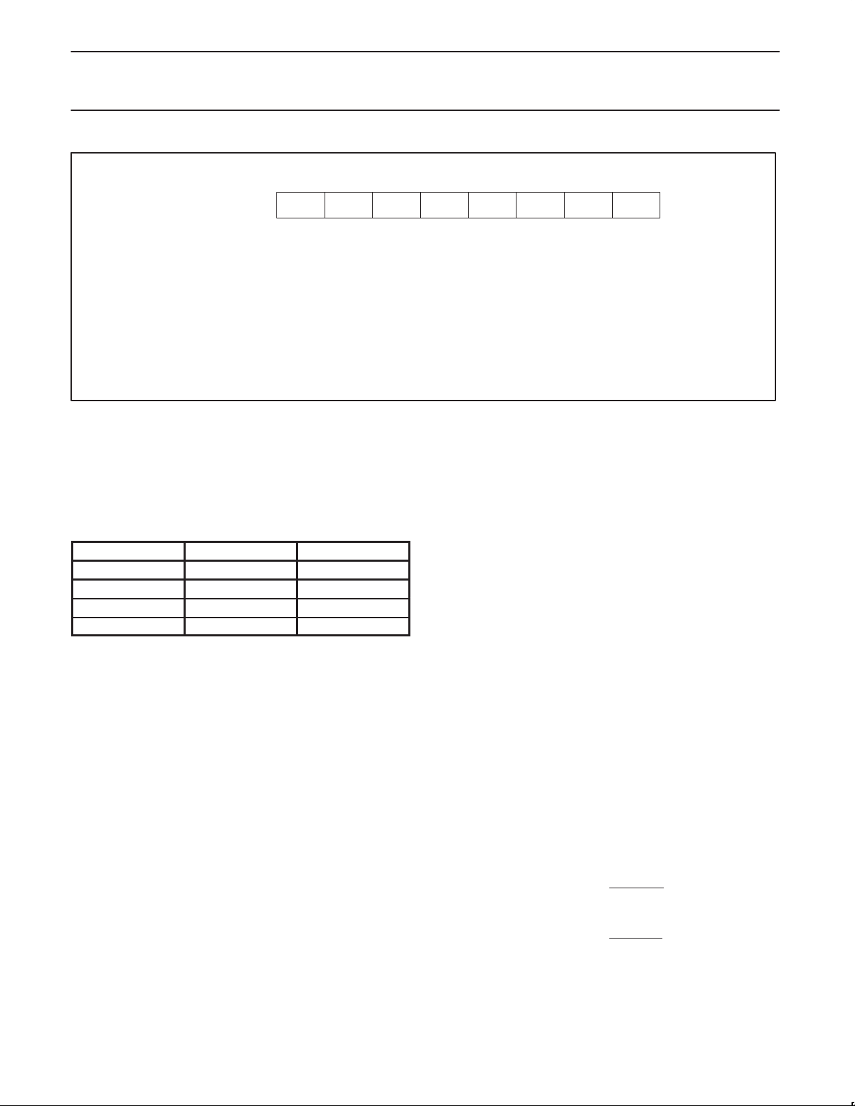
Philips Semiconductors Preliminary specification
XA 16-bit microcontroller
32 K/1 K OTP/ROM/ROMless, 8-channel 8-bit A/D, low voltage (2.7 V–5.5 V),
2
C, 2 UARTs, 16 MB address range
I
XA-S3
SnSTAT Address: S0STAT 421
S1STAT 425
Bit Addressable
Reset Value: 00H
BIT SYMBOL FUNCTION
SnSTAT.3 FEn Framing Error flag is set when the receiver fails to see a valid STOP bit at the end of the frame.
Cleared by software.
SnSTAT.2 BRn Break Detect flag is set if a character is received with all bits (including STOP bit) being logic ‘0’. Thus
it gives a “Start of Break Detect” on bit 8 for Mode 1 and bit 9 for Modes 2 and 3. The break detect
feature operates independently of the UARTs and provides the START of Break Detect status bit that
a user program may poll. Cleared by software.
SnSTAT.1 OEn Overrun Error flag is set if a new character is received in the receiver buffer while it is still full (before
the software has read the previous character from the buffer), i.e., when bit 8 of a new byte is
received while RI in SnCON is still set. Cleared by software.
SnSTAT.0 STINTn This flag must be set to enable any of the above status flags to generate a receive interrupt (RIn). The
only way it can be cleared is by a software write to this register.
Figure 20. Serial Port Extended Status (SnSTAT) Register
(See also Figure 22 regarding Framing Error flag)
UART INTERRUPT SCHEME
There are separate interrupt vectors for each UART’s transmit and
receive functions.
Table 5. Interrupt Vector Locations for UARTs
Vector Address Interrupt Source Arbitration
A0H – A3H UART 0 Receiver 9
A4H – A7H UART 0 Transmitter 10
A8H – ABH UAR T 1 Receiver 11
ACH – AFH UART 1 Transmitter 12
NOTE:
The transmit and receive vectors could contain the same ISR
address to work like a 8051 interrupt scheme
Error Handling, Status Flags and Break Detect
XA UARTs have several error flags as described in Figures 20 and
22.
Multiprocessor Communications
Modes 2 and 3 have a special provision for multiprocessor
communications. In these modes, 9 data bits are received. The 9th
one goes into RB8. Then comes a stop bit. The port can be
programmed such that when the stop bit is received, the serial port
interrupt will be activated only if RB8 = 1. This feature is enabled by
setting bit SM2 in SCON. A way to use this feature in multiprocessor
systems is as follows:
When the master processor wants to transmit a block of data to one
of several slaves, it first sends out an address byte which identifies
the target slave. An address byte differs from a data byte in that the
9th bit is 1 in an address byte and 0 in a data byte. With SM2 = 1, no
slave will be interrupted by a data byte. An address byte, however,
will interrupt all slaves, so that each slave can examine the received
byte and see if it is being addressed. The addressed slave will clear
its SM2 bit and prepare to receive the data bytes that will be coming.
The slaves that weren’t being addressed leave their SM2s set and
go on about their business, ignoring the coming data bytes.
SM2 has no effect in Mode 0, and in Mode 1 can be used to check
the validity of the stop bit although this is better done with the Framing
LSBMSB
STINTn
OEnBRnFEn————
SU00607B
Error (FE) flag. In a Mode 1 reception, if SM2 = 1, the receive
interrupt will not be activated unless a valid stop bit is received.
Automatic Address Recognition
Automatic Address Recognition is a feature which allows the UART
to recognize certain addresses in the serial bit stream by using
hardware to make the comparisons. This feature saves a great deal
of software overhead by eliminating the need for the software to
examine every serial address which passes by the serial port. This
feature is enabled by setting the SM2 bit in SCON. In the 9 bit UART
modes, mode 2 and mode 3, the Receive Interrupt flag (RI) will be
automatically set when the received byte contains either the “Given”
address or the “Broadcast” address. The 9 bit mode requires that
the 9th information bit is a 1 to indicate that the received information
is an address and not data. Automatic address recognition is shown
in Figure 23.
Using the Automatic Address Recognition feature allows a master to
selectively communicate with one or more slaves by invoking the
Given slave address or addresses. All of the slaves may be
contacted by using the Broadcast address. Two special Function
Registers are used to define the slave’s address, SADDR, and the
address mask, SADEN. SADEN is used to define which bits in the
SADDR are to be used and which bits are “don’t care”. The SADEN
mask can be logically ANDed with the SADDR to create the “Given”
address which the master will use for addressing each of the slaves.
Use of the Given address allows multiple slaves to be recognized
while excluding others. The following examples will help to show the
versatility of this scheme:
Slave 0 SADDR = 1100 0000
Slave 1 SADDR = 1100 0000
In the above example SADDR is the same and the SADEN data is
used to differentiate between the two slaves. Slave 0 requires a 0 in
bit 0 and it ignores bit 1. Slave 1 requires a 0 in bit 1 and bit 0 is
ignored. A unique address for Slave 0 would be 1100 0010 since
slave 1 requires a 0 in bit 1. A unique address for slave 1 would be
SADEN = 1111 1101
Given = 1100 00X0
SADEN = 1111 1110
Given = 1100 000X
2000 Aug 22
29
Page 30

Philips Semiconductors Preliminary specification
XA 16-bit microcontroller
32 K/1 K OTP/ROM/ROMless, 8-channel 8-bit A/D, low voltage (2.7 V–5.5 V),
2
C, 2 UARTs, 16 MB address range
I
XA-S3
1100 0001 since a 1 in bit 0 will exclude slave 0. Both slaves can be
selected at the same time by an address which has bit 0 = 0 (for
slave 0) and bit 1 = 0 (for slave 1). Thus, both could be addressed
with 1100 0000.
In a more complex system the following could be used to select
slaves 1 and 2 while excluding slave 0:
Slave 0 SADDR = 1100 0000
SADEN = 1111 1001
Given = 1100 0XX0
Slave 1 SADDR = 1110 0000
SADEN = 1111 1010
Given = 1110 0X0X
Slave 2 SADDR = 1110 0000
SADEN = 1111 1100
Given = 1110 00XX
SnCON Address: S0CON 420
S1CON 424
Bit Addressable
Reset Value: 00H
Where SM0, SM1 specify the serial port mode, as follows:
SM0 SM1 Mode Description Baud Rate
0 0 0 shift register f
0 1 1 8-bit UART variable
1 0 2 9-bit UART f
1 1 3 9-bit UART variable
In the above example the differentiation among the 3 slaves is in the
lower 3 address bits. Slave 0 requires that bit 0 = 0 and it can be
uniquely addressed by 1110 01 10. Slave 1 requires that bit 1 = 0 and
it can be uniquely addressed by 1110 and 0101. Slave 2 requires
that bit 2 = 0 and its unique address is 1110 0011. To select Slaves 0
and 1 and exclude Slave 2 use address 1110 0100, since it is
necessary to make bit 2 = 1 to exclude slave 2.
The Broadcast Address for each slave is created by taking the
logical OR of SADDR and SADEN. Zeros in this result are teated as
don’t-cares. In most cases, interpreting the don’t-cares as ones, the
broadcast address will be FF hexadecimal.
Upon reset SADDR and SADEN are loaded with 0s. This produces
a given address of all “don’t cares” as well as a Broadcast address
of all “don’t cares”. This effectively disables the Automatic
Addressing mode and allows the microcontroller to use standard
UART drivers which do not make use of this feature.
LSBMSB
RITIRB8TB8RENSM2SM1SM0
/16
OSC
/32
OSC
BIT SYMBOL FUNCTION
SnCON.5 SM2 Enables the multiprocessor communication feature in Modes 2 and 3. In Mode 2 or 3, if SM2 is set to 1, then RI
SnCON.4 REN Enables serial reception. Set by software to enable reception. Clear by software to disable reception.
SnCON.3 TB8 The 9th data bit that will be transmitted in Modes 2 and 3. Set or clear by software as desired. The TB8 bit is not
SnCON.2 RB8 In Modes 2 and 3, is the 9th data bit that was received. In Mode 1, if SM2=0, RB8 is the stop bit that was
SnCON.1 TI Transmit interrupt flag. Set when another byte may be written to the UART transmitter. See text for details.
SnCON.0 RI Receive interrupt flag. Set by hardware at the end of the 8th bit time in Mode 0, or at the end of the stop bit time
will not be activated if the received 9th data bit (RB8) is 0. In Mode 1, if SM2=1 then RI will not be activated if a
valid stop bit was not received. In Mode 0, SM2 should be 0.
double buffered. See text for details.
received. In Mode 0, RB8 is not used.
Must be cleared by software.
in the other modes (except see SM2). Must be cleared by software.
SU00597C
Figure 21. Serial Port Control (SnCON) Register
2000 Aug 22
30
Page 31
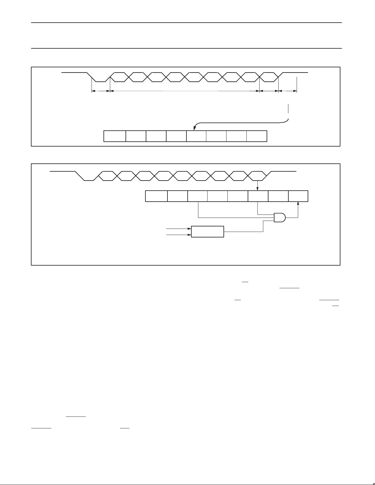
Philips Semiconductors Preliminary specification
XA 16-bit microcontroller
32 K/1 K OTP/ROM/ROMless, 8-channel 8-bit A/D, low voltage (2.7 V–5.5 V),
2
C, 2 UARTs, 16 MB address range
I
D0 D1 D2 D3 D4 D5 D6 D7 D8
XA-S3
START
BIT
— — — — FEn BRn OEn STINTn
DATA BYTE
ONLY IN
MODE 2, 3
SnSTAT
Figure 22. UART Framing Error Detection
D0 D1 D2 D3 D4 D5 D6 D7 D8
SM0_n SM1_n SM2_n REN_n TB8_n RB8_n TI_n RI_n
1
1
RECEIVED ADDRESS D0 TO D7
PROGRAMMED ADDRESS
IN UART MODE 2 OR MODE 3 AND SM2 = 1:
INTERRUPT IF REN=1, RB8=1 AND “RECEIVED ADDRESS” = “PROGRAMMED ADDRESS”
– WHEN OWN ADDRESS RECEIVED, CLEAR SM2 TO RECEIVE DATA BYTES
– WHEN ALL DATA BYTES HAVE BEEN RECEIVED: SET SM2 TO WAIT FOR NEXT ADDRESS.
1
0
11 X
COMPARATOR
Figure 23. UART Multiprocessor Communication, Automatic Address Recognition
STOP
BIT
if 0, sets FE
SU00598
SnCON
SU00613
Clocking / Baud Rate Generation
Same as for the XA-G3.
I/O Port Output Configuration
Port output configurations are the same as for the XA-G3: open
drain, quasi-bidirectional, push-pull, and off.
External Bus
The external bus operates in the same manner as the XA-G3, but
all 24 address lines are brought out to the outside world. This
allows for a maximum of 16 Mbytes of code memory and 16
Mbytes of data memory.
Clock Output
The CLKOUT pin allows easier external bus interfacing in some
situations. This output reflects the X1 clock input to the XA, but is
delayed to match the external bus outputs and strobes. The default
is for CLKOUT to be on at reset, but it may be turned off via the
CLKD bit that has been added to the BCR register.
Reset
Active low reset input, the same as the XA-G3.
The associated RSTOUT
active low open drain output when an internal reset occurs. The
RSTOUT
pin will be driven low when the RST pin is driven low,
when a Watchdog reset occurs or the RESET instruction is
executed. This signal may be used to inform other devices in a
system that the XA-S3 has been reset.
pin provides an external indication via an
The latched values of EA
updated when an internal reset occurs. RSTOUT
and BUSW are NOT automatically
may be used to
apply an external reset to the XA-S3 in order to update the
previously latched EA
and BUSW values. However, since RSTOUT
reflects ALL reset sources, it cannot simply be fed back into the RST
pin without other logic.
The reset source identification register (RSTSRC) indicates the cause
of the most recent XA reset. The cause may have been an externally
applied reset signal, execution of the RESET instruction, or a
Watchdog reset. Figure 24 shows the fields in the RSTSRC register.
Power Reduction Modes
The XA-S3 supports Idle and Power Down modes of power
reduction. The idle mode leaves some peripherals running in order
to allow them to activate the processor when an interrupt is
generated. The power down mode stops the oscillator in order to
absolutely minimize power . The processor can be made to exit
power down mode via a reset or one of the external interrupt inputs
(INT0 or INT1). This will occur if the interrupt is enabled and its
priority is higher than that defined by IM3 through IM0. In power
down mode, the power supply voltage may be reduced to the RAM
keep-alive voltage V
contents at the point where power down mode was entered. V
must be raised to within the operating range before power down
mode is exited.
. This retains the RAM, register, and SFR
RAM
DD
2000 Aug 22
31
Page 32
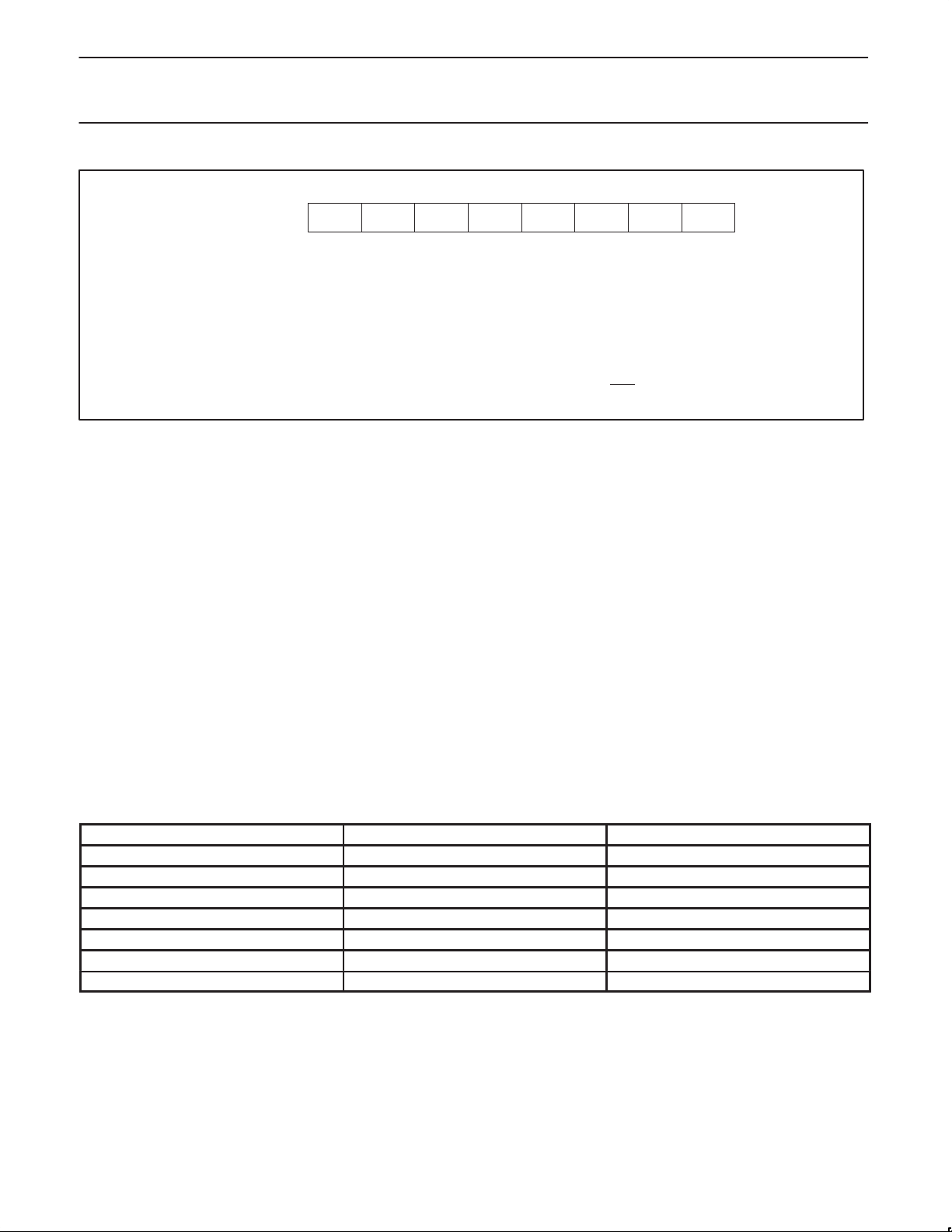
Philips Semiconductors Preliminary specification
XA 16-bit microcontroller
32 K/1 K OTP/ROM/ROMless, 8-channel 8-bit A/D, low voltage (2.7 V–5.5 V),
2
C, 2 UARTs, 16 MB address range
I
XA-S3
RSTSRC Address:463h
Not bit Addressable
Reset Value: see below
BIT SYMBOL FUNCTION
RSTSRC.7 — Reserved for future use. Should not be set to 1 by user programs.
RSTSRC.6 — Reserved for future use. Should not be set to 1 by user programs.
RSTSRC.5 — Reserved for future use. Should not be set to 1 by user programs.
RSTSRC.4 — Reserved for future use. Should not be set to 1 by user programs.
RSTSRC.3 — Reserved for future use. Should not be set to 1 by user programs.
RSTSRC.2 R_WD Indicates that the last reset was caused by a watchdog timer overflow.
RSTSRC.1 R_CMD Indicates that the last reset was caused by execution of the RESET instruction.
RSTSRC.0 R_EXT Indicates that the last reset was caused by the external RST
Figure 24. Reset source register (RSTSRC)
INTERRUPTS
XA-S3 interrupt sources include the following:
•External interrupts 0 and 1 (2)
•Timer 0, 1, and 2 interrupts (3)
•PCA: 1 global and 5 channel interrupts (6)
•A/D interrupt (1)
•UART 0 transmitter and receiver interrupts (2)
•UART 1 transmitter and receiver interrupts (2)
2
•I
C interrupt (1)
•Software interrupts (7)
There are a total of 17 hardware interrupt sources, enable bits,
priority bit sets, etc.
The XA-S3 supports a total of 17 maskable event interrupt sources
(for the various XA peripherals), seven software interrupts, 5
LSBMSB
————
exception interrupts (plus reset), and 16 traps. The maskable event
interrupts share a global interrupt disable bit (the EA bit in the IEL
register) and each also has a separate individual interrupt enable bit
(in the IEL or IEH registers). Only three bits of the IPA register
values are used on the XA-S3. Each event interrupt can be set to
occur at one of 8 priority levels via bits in the Interrupt Priority (IP)
registers, IPA0 through IPA5. The value 0 in the IPA field gives the
interrupt priority 0, in effect disabling the interrupt. A value of 1 gives
the interrupt a priority of 9, the value 2 gives priority 10, etc. The
result is the same as if all four bits were used and the top bit set for
all values except 0. Details of the priority scheme may be found in
the
The complete interrupt vector list for the XA-S3, including all
4 interrupt types, is shown in the following tables. The tables include
the address of the vector for each interrupt, the related priority
register bits (if any), and the arbitration ranking for that interrupt
source. The arbitration ranking determines the order in which
interrupts are processed if more than one interrupt of the same
priority occurs simultaneously.
— R_WD R_CMD R_EXT
input.
XA User Guide
.
SU00942
EXCEPTION/TRAPS PRECEDENCE
DESCRIPTION VECTOR ADDRESS ARBITRATION RANKING
Reset (h/w, watchdog, s/w) 0000–0003 0 (High)
Breakpoint 0004–0007 1
Trace 0008–000B 1
Stack Overflow 000C–000F 1
Divide by 0 0010–0013 1
User RETI 0014–0017 1
TRAP 0–15 (software) 0040–007F 1
2000 Aug 22
32
Page 33
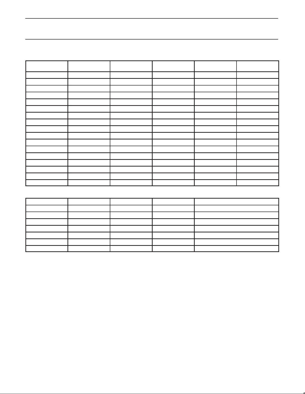
Philips Semiconductors Preliminary specification
XA 16-bit microcontroller
32 K/1 K OTP/ROM/ROMless, 8-channel 8-bit A/D, low voltage (2.7 V–5.5 V),
2
C, 2 UARTs, 16 MB address range
I
EVENT INTERRUPTS
DESCRIPTION FLAG BIT VECTOR ADDRESS ENABLE BIT
External Interrupt 0 IE0 0080–0083 EX0 IPA0.2–0 (PX0) 2
Timer 0 Interrupt TF0 0084–0087 ET0 IPA0.6–4 (PT0) 3
External Interrupt 1 IE1 0088–008B EX1 IPA1.2–0 (PX1) 4
Timer 1 Interrupt TF1 008C–008F ET1 IPA1.6–4 (PT1) 5
Timer 2 Interrupt TF2 (EXF2) 0090–0093 ET2 IPA2.2–0 (PT2) 6
PCA Interrupt CCF0–CCF4, CF 0094–0097 EPC IPA2.6–4 (PPC) 7
A/D Interrupt ADINT 0098–009B EAD IPA3.2–0 (PAD) 8
Serial Port 0 Rx RI_0 00A0–00A3 ERI0 IPA4.2–0 (PRI0) 9
Serial Port 0 Tx TI_0 00A4–00A7 ETI0 IPA4.6–4 (PTI0) 10
Serial Port 1 Rx RI_1 00A8–00AB ERI1 IPA5.2–0 (PRI1) 11
Serial Port 1 Tx TI_1 00AC–00AF ETI1 IPA5.6–4 (PTI1) 12
PCA channel 0 CCF0 00C0–00C3 EC0 IPB0.2–0 (PC0) 17
PCA channel 1 CCF1 00C4–00C7 EC1 IPB0.6–4 (PC1) 18
PCA channel 2 CCF2 00C8–00CB EC2 IPB1.2–0 (PC2) 19
PCA channel 3 CCF3 00CC–00CF EC3 IPB1.6–4 (PC3) 20
PCA channel 4 CCF4 00D0–00D3 EC4 IPB2.2–0 (PC4) 21
I2C Interrupt SI 00D4–00D7 EI2 IPB2.6–4 (PI2) 22
INTERRUPT
PRIORITY
XA-S3
ARBITRATION
RANKING
SOFTWARE INTERRUPTS
DESCRIPTION FLAG BIT VECTOR ADDRESS ENABLE BIT INTERRUPT PRIORITY
Software Interrupt 1 SWR1 0100–0103 SWE1 (fixed at 1)
Software Interrupt 2 SWR2 0104–0107 SWE2 (fixed at 2)
Software Interrupt 3 SWR3 0108–010B SWE3 (fixed at 3)
Software Interrupt 4 SWR4 010C–010F SWE4 (fixed at 4)
Software Interrupt 5 SWR5 01 10–0113 SWE5 (fixed at 5)
Software Interrupt 6 SWR6 01 14–0117 SWE6 (fixed at 6)
Software Interrupt 7 SWR7 0118–011B SWE7 (fixed at 7)
2000 Aug 22
33
Page 34
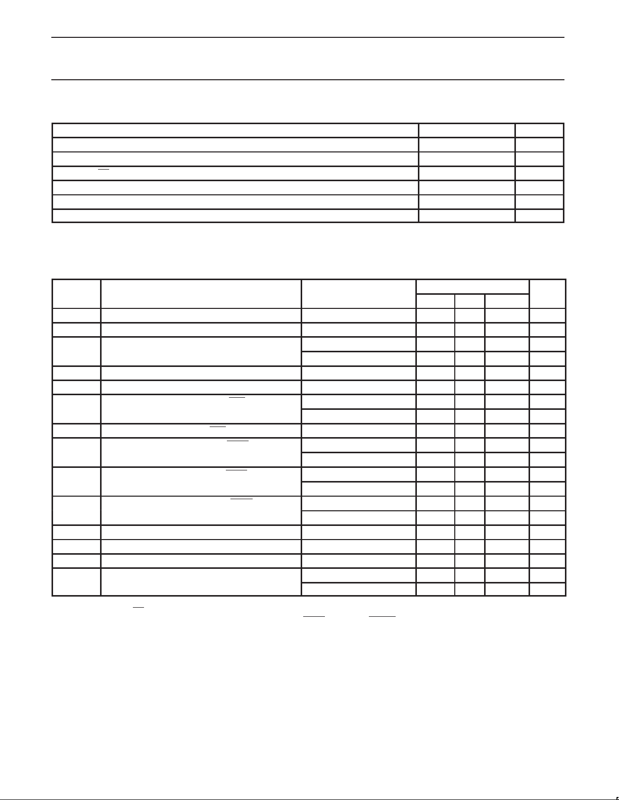
Philips Semiconductors Preliminary specification
SYMBOL
PARAMETER
TEST CONDITIONS
UNIT
5
XA 16-bit microcontroller
32 K/1 K OTP/ROM/ROMless, 8-channel 8-bit A/D, low voltage (2.7 V–5.5 V),
2
C, 2 UARTs, 16 MB address range
I
ABSOLUTE MAXIMUM RATINGS
PARAMETER RATING UNIT
Operating temperature under bias –55 to +125 °C
Storage temperature range –65 to +150 °C
Voltage on EA/VPP pin to V
Voltage on any other pin to V
SS
SS
0 to +13.0 V
–0.5 to VDD+0.5 V V
Maximum IOL per I/O pin 15 mA
Power dissipation (based on package heat transfer, not device power consumption) 1.5 W
DC ELECTRICAL CHARACTERISTICS
VDD = 2.7 V to 5.5 V, unless otherwise specified.
= 0 to +70°C for commercial, T
T
amb
I
I
I
V
V
V
V
V
V
V
C
I
I
I
DD
ID
PD
RAM
IL
IH
IH1
OL
OH1
OH2
IO
IL
LI
TL
Power supply current, operating 5.0 V, 30 MHz 80 mA
Power supply current, Idle mode 5.0 V, 30 MHz 35 mA
Power supply current, Power Down mode
RAM keep-alive voltage 1.5 V
Input low voltage –0.5 0.22 V
Input high voltage, except XTAL1, RST
Input high voltage to XTAL1, RST For both 3.0 V and 5.0 V 0.7 V
Output low voltage, all ports, ALE, PSEN4, CLKOUT
Output high voltage, all ports, ALE, PSEN2, CLKOUT
Output high voltage, all ports ALE, PSEN3, CLKOUT
Input/Output pin capacitance
Logical 0 input current, all ports
Input leakage current, all ports
Logical 1 to 0 transition current, all ports
NOTES:
1. Maximum 15pF for EA
/VPP.
2. Ports in quasi-bidirectional mode with weak pullup (applies to ALE, PSEN
3. Ports in PUSH-PULL mode, both pullup and pulldown assumed to be the same strength.
4. In all output modes.
5. Port pins source a transition current when used in quasi-bidirectional mode and externally driven from 1 to 0. This current is highest when
is approximately 2 V.
V
IN
6. Measured with port in high impedance mode.
7. Measured with port in quasi-bidirectional mode.
8. Under steady state (non-transient) conditions, I
Maximum I
Maximum I
Maximum total I
If I
exceeds the test condition, VOL may exceed the related specification. Pins are not guaranteed to sink current greater than the listed
OL
test conditions.
per port pin: 15 mA
OL
per 8-bit port: 26 mA
OL
for all outputs: 71 mA
OL
= –40°C to +85°C for industrial, unless otherwise specified.
amb
5.0 V, 3.0 V 5 100 µA
5.0 V , 3.0 V, –40 to +85°C 150 µA
VDD = 5.0 V 2.2 V
VDD = 3.0 V 2.0 V
IOL = 3.2 mA, VDD = 5.0 V 0.5 V
IOL = 1.0 mA, VDD = 3.0 V 0.4 V
IOH = –100 µA, VDD = 4.5 V 2.4 V
IOH = –30 µA, VDD = 2.7 V 2.0 V
IOH = –3.2 mA, VDD = 4.5 V 2.4 V
IOH = –1.0 mA, VDD = 2.7 V 2.2 V
1
7
6
VIN = 0.45 V –50 µA
VIN = VIL or V
At VDD = 5.5 V –650 µA
At VDD = 2.7 V –250 µA
only during RESET).
must be externally limited as follows:
OL
LIMITS
MIN TYP MAX
DD
IH
XA-S3
DD
15 pF
±10 µA
V
V
2000 Aug 22
34
Page 35
Philips Semiconductors Preliminary specification
SYMBOL
PARAMETER
TEST CONDITIONS
UNIT
XA 16-bit microcontroller
32 K/1 K OTP/ROM/ROMless, 8-channel 8-bit A/D, low voltage (2.7 V–5.5 V),
2
C, 2 UARTs, 16 MB address range
I
8-BIT MODE A/D CONVERTER DC ELECTRICAL CHARACTERISTICS
T
= 0 to +70°C for commercial, T
amb
AV
AI
AI
AI
AV
R
C
DL
IL
OS
G
A
M
C
DD
DD
ID
PD
IN
REF
IA
e
e
e
e
e
CTC
t
Analog supply voltage 2.7 3.3 V
Analog supply current (operating) Port 5 = 0 to AV
Analog supply current (Idle mode) 2.5 µA
Analog supply current (Power-Down mode)
Analog input voltage AVSS –0.2 AVDD +0.2 V
Resistance between V
Analog input capacitance 15 pF
Differential non-linearity
Integral non-linearity
Offset error
Gain error
1, 5
1, 6
Absolute voltage error
Channel-to-channel matching ±1 LSB
Crosstalk between inputs of port
NOTES:
1. Conditions: AV
2. The differential non-linearity (DL
REF–
= 0 V; AV
3. The ADC is monotonic, there are no missing codes.
4. The integral non-linearity (IL
appropriate adjustment of gain and offset errors. See Figure 25.
5. The offset error (OS
the straight line which fits the ideal transfer curve. See Figure 25.
6. The gain error (G
and the straight line which fits the ideal transfer curve. Gain error is constant at every point on the transfer curve. See Figure 25.
) is the relative difference in percent between the straight line fitting the actual transfer curve (after removing offset error),
e
e
) is the absolute difference between the straight line which fits the actual transfer curve (after removing gain error), and
e
7. The absolute voltage error (A
ADC and the ideal transfer curve.
8. This should be considered when both analog and digital signals are input simultaneously to Port 5. Parameter is guaranteed by design.
= –40 to +85°C for industrial, unless otherwise specified.
amb
LIMITS
MIN MAX
DD
2.5 mA
Commercial temperature range 100 µA
Industrial temperature range 150 µA
1, 4
REF+
1, 2, 3
and V
REF–
125 225 kΩ
±1 LSB
±1 LSB
±2.5 LSB
±1 %
1, 7
8
= 3.07 V.
REF+
) is the difference between the actual step width and the ideal step width. See Figure 25.
e
0 – 100 kHz –60 dB
±3 LSB
) is the peak difference between the center of the steps of the actual and the ideal transfer curve after
) is the maximum difference between the center of the steps of the actual transfer curve of the non-calibrated
e
XA-S3
2000 Aug 22
35
Page 36
Philips Semiconductors Preliminary specification
SYMBOL
PARAMETER
TEST CONDITIONS
UNIT
XA 16-bit microcontroller
32 K/1 K OTP/ROM/ROMless, 8-channel 8-bit A/D, low voltage (2.7 V–5.5 V),
2
C, 2 UARTs, 16 MB address range
I
10-BIT10 MODE A/D CONVERTER DC ELECTRICAL CHARACTERISTICS
T
= 0 to +70°C for commercial, T
amb
AV
AI
AI
AI
AV
R
C
DL
IL
OS
G
A
M
C
DD
DD
ID
PD
IN
REF
IA
e
e
e
e
e
CTC
t
Analog supply voltage 2.7 3.3 V
Analog supply current (operating) Port 5 = 0 to AV
Analog supply current (Idle mode) 2.5 µA
Analog supply current (Power-Down mode)
Analog input voltage AVSS –0.2 AVDD +0.2 V
Resistance between V
Analog input capacitance 15 pF
Differential non-linearity
Integral non-linearity
Offset error
Gain error
1, 5
1, 6
Absolute voltage error (with averaging)
Channel-to-channel matching ±1 LSB
Crosstalk between inputs of port
NOTES:
1. Conditions: AV
2. The differential non-linearity (DL
REF–
= 0 V; AV
3. The ADC is monotonic, there are no missing codes.
4. The integral non-linearity (IL
appropriate adjustment of gain and offset errors. See Figure 25.
5. The offset error (OS
the straight line which fits the ideal transfer curve. See Figure 25.
6. The gain error (G
and the straight line which fits the ideal transfer curve. Gain error is constant at every point on the transfer curve. See Figure 25.
) is the absolute difference between the straight line which fits the actual transfer curve (after removing gain error), and
e
) is the relative difference in percent between the straight line fitting the actual transfer curve (after removing offset error),
e
7. The absolute voltage error (A
ADC and the ideal transfer curve.
8. This should be considered when both analog and digital signals are input simultaneously to Port 5. Parameter is guaranteed by design.
9. 10-bit mode only.
10.10-bit mode is only operational up to f
= –40 to +85°C for industrial, unless otherwise specified.
amb
LIMITS
MIN MAX
DD
2.5 mA
Commercial temperature range 100 µA
Industrial temperature range 150 µA
1, 4
REF+
1, 2, 3
and V
REF–
125 225 kΩ
±1
±2.5
±6
±1
1, 7
8
= 3.07 V.
REF+
) is the difference between the actual step width and the ideal step width. See Figure 25.
e
) is the peak difference between the center of the steps of the actual and the ideal transfer curve after
e
) is the maximum difference between the center of the steps of the actual transfer curve of the non-calibrated
e
= 20 MHz.
C
0 – 100 kHz –60 dB
±8
9
9
9
9
9
XA-S3
LSB
LSB
LSB
%
LSB
2000 Aug 22
36
Page 37
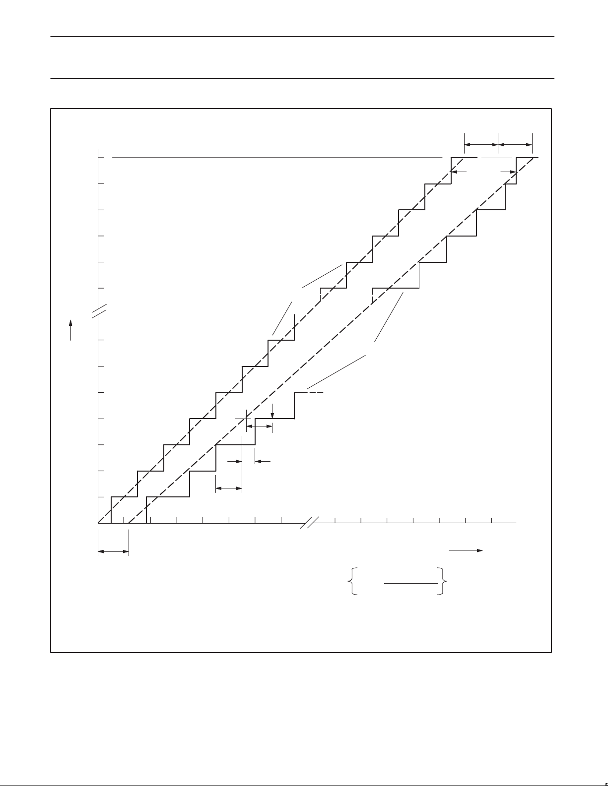
Philips Semiconductors Preliminary specification
XA 16-bit microcontroller
32 K/1 K OTP/ROM/ROMless, 8-channel 8-bit A/D, low voltage (2.7 V–5.5 V),
2
C, 2 UARTs, 16 MB address range
I
XA-S3
Code
Out
255
254
253
252
251
250
Offset
error
OS
Full Scale
(2)
7
6
5
(5)
4
(4)
3
(1)
e
error
FS
Gain
error
G
e
e
2
1
0
1 2 3 4 5 6 7 250 251 252 253 254 255 256
Offset
error
OS
e
(1) Example of an actual transfer curve.
(2) The ideal transfer curve.
(3) Differential non-linearity (DL
(4) Integral non-linearity (IL
(5) Center of a step of the actual transfer curve.
).
e
).
e
(3)
1 LSB
(ideal)
1 LSB =
Figure 25. ADC Conversion Characteristic
AV
REF+
AVIN (LSB
– AV
256
ideal
REF–
)
SU01010
2000 Aug 22
37
Page 38
Philips Semiconductors Preliminary specification
SYMBOL
FIGURE
PARAMETER
UNIT
XA 16-bit microcontroller
32 K/1 K OTP/ROM/ROMless, 8-channel 8-bit A/D, low voltage (2.7 V–5.5 V),
2
C, 2 UARTs, 16 MB address range
I
AC ELECTRICAL CHARACTERISTICS (5 V)
VDD = 4.5 V to 5.5 V; T
External Clock
f
C
t
C
t
CHCX
t
CLCX
t
CLCH
t
CHCL
Address Cycle
t
LHLL
t
AVLL
t
LLAX
26, 28, 30 ALE pulse width (programmable) (V1 * tC) – 6 ns
26, 28, 30 Address valid to ALE de-asserted (set-up) (V1 * tC) – 12 ns
26, 28, 30 Address hold after ALE de-asserted (tC/2) – 10 ns
Code Read Cycle
t
PLPH
t
LLPL
t
AVIVA
t
AVIVB
t
PLIV
t
PHIX
t
PHIZ
t
IXUA
Data Read Cycle
t
RLRH
t
LLRL
t
AVDVA
t
AVDVB
t
RLDV
t
RHDX
t
RHDZ
t
DXUA
Data Write Cycle
t
WLWH
t
LLWL
t
QVWX
t
WHQX
t
AVWL
t
UAWH
Wait Input
t
WTH
t
WTL
NOTES ON PAGE 41.
= 0 to +70°C for commercial, T
amb
= –40°C to +85°C for industrial.
amb
32 Oscillator frequency 0 30 MHz
32 Clock period and CPU timing cycle 1/f
32 Clock high-time (Note 7) tC * 0.5 ns
32 Clock low time (Note 7) tC * 0.4 ns
32 Clock rise time (Note 7) 5 ns
32 Clock fall time (Note 7) 5 ns
26 PSEN pulse width (V2 * tC) – 10 ns
26 ALE de-asserted to PSEN asserted (tC/2) – 7 ns
26 Address valid to instruction valid, ALE cycle (access time) (V3 * tC) – 36 ns
27 Address valid to instruction valid, non-ALE cycle (access time) (V4 * tC) – 29 ns
26 PSEN asserted to instruction valid (enable time) (V2 * tC) – 29 ns
26 Instruction hold after PSEN de-asserted 0 ns
26 Bus 3-State after PSEN de-asserted tC – 8 ns
26 Hold time of unlatched part of address after instruction latched 0 ns
28 RD pulse width (V7 * tC) – 10 ns
28 ALE de-asserted to RD asserted (tC/2) – 7 ns
28 Address valid to data input valid, ALE cycle (access time) (V6 * tC) – 36 ns
29 Address valid to data input valid, non-ALE cycle (access time) (V5 * tC) – 29 ns
28 RD low to valid data in (enable time) (V7 * tC) – 29 ns
28 Data hold time after RD de–asserted 0 ns
28 Bus 3-State after RD de-asserted (disable time) tC – 8 ns
28 Hold time of unlatched part of address after data latched 0 ns
30 WR pulse width (V8 * tC) – 10 ns
30 ALE falling edge to WR asserted (V12 * tC) – 10 ns
30 Data valid before WR asserted (data set-up time) (V13 * tC) – 22 ns
30 Data hold time after WR de-asserted (Note 6) (V11 * tC) – 5 ns
30 Address valid to WR asserted (address set-up time) (Note 5) (V9 * tC) – 22 ns
30 Hold time of unlatched part of address after WR is de-asserted (V11 * tC) – 7 ns
31 WAIT stable after bus strobe (RD, WR, or PSEN) asserted (V10 * tC) – 30 ns
31 WAIT hold after bus strobe (RD, WR, or PSEN) asserted (V10 * tC) – 5 ns
LIMITS
MIN MAX
C
XA-S3
ns
2000 Aug 22
38
Page 39
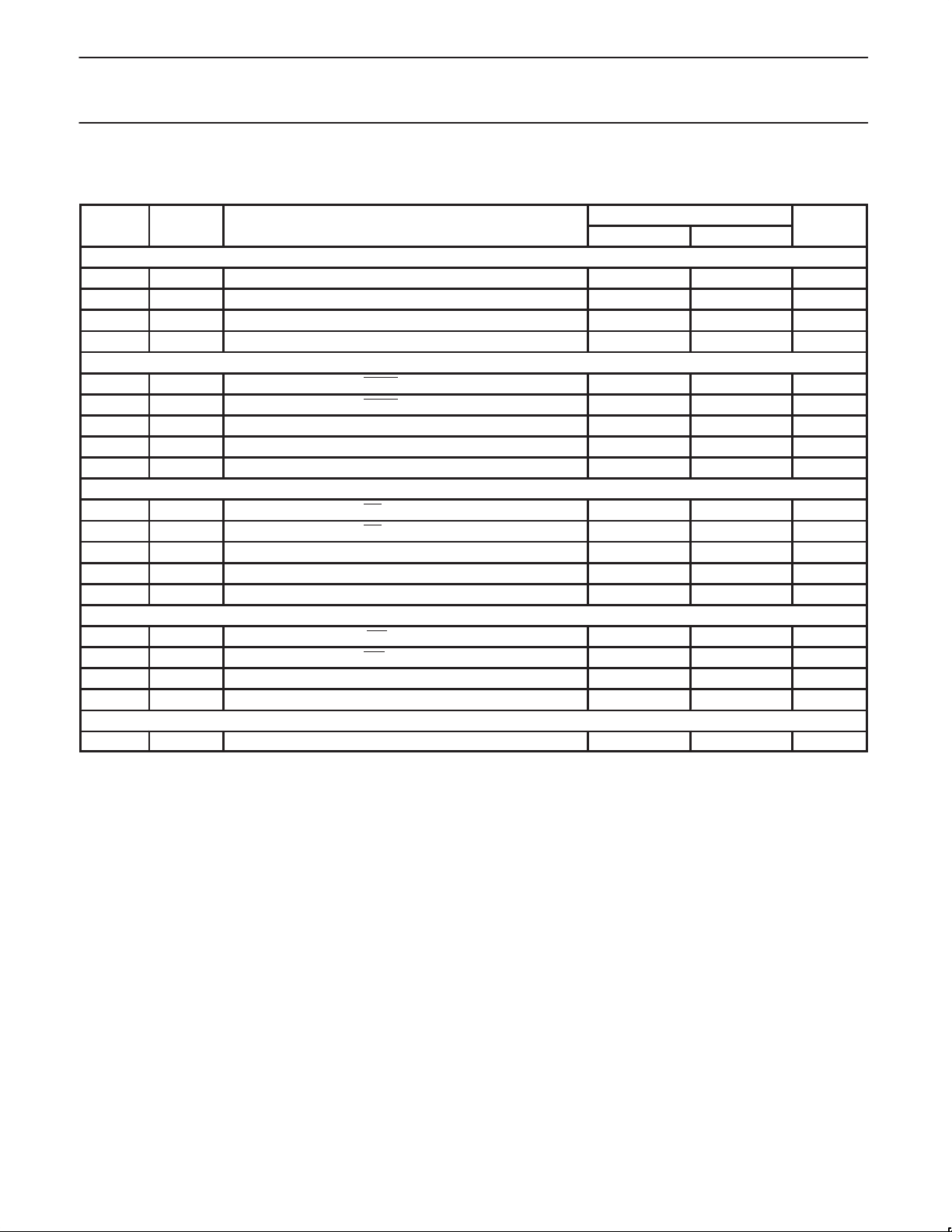
Philips Semiconductors Preliminary specification
SYMBOL
FIGURE
PARAMETER
UNIT
XA 16-bit microcontroller
32 K/1 K OTP/ROM/ROMless, 8-channel 8-bit A/D, low voltage (2.7 V–5.5 V),
2
C, 2 UARTs, 16 MB address range
I
AC ELECTRICAL CHARACTERISTICS (5 V RANGE) (continued)
This set of parameters is referenced to the XA-S3 clock output.
Address Cycle
t
CHLH
t
CLLL
t
CHAV
t
CHAX
Code Read Cycle
t
CHPL
t
CHPH
t
IVCH
t
CHIX
t
CHIZ
Data Read Cycle
t
CHRL
t
CHRH
t
DVCH
t
CHDX
t
CHDZ
Data Write Cycle
t
CHWL
t
CHWH
t
QVCH
t
CHQX
Wait Input
t
CHWTH
NOTES ON PAGE 41.
26 CLKOUT rising edge to ALE rising edge – 13 ns
26 CLKOUT falling edge to ALE falling edge – 9 ns
26 CLKOUT rising edge to address valid – 18 ns
26 CLKOUT rising edge to address changing (hold time) 2 – ns
26 CLKOUT rising edge to PSEN asserted – 14 ns
26 CLKOUT rising edge to PSEN de-asserted – 12 ns
26 Instruction valid to CLKOUT rising edge (setup time) 20 – ns
26 CLKOUT rising edge to instruction changing (hold time) 0 – ns
26 CLKOUT rising edge to Bus 3-State (code read) – tC–8 ns
28 CLKOUT rising edge to RD asserted – 12 ns
28 CLKOUT rising edge to RD de-asserted – 10 ns
28 Data valid to CLKOUT rising edge (setup time) 20 – ns
28 CLKOUT rising edge to Data changing (hold time) 0 – ns
28 CLKOUT rising edge to Bus 3-State (data read) – tC–8 ns
30 CLKOUT falling edge to WR asserted – 12 ns
30 CLKOUT rising edge to WR de-asserted – 10 ns
30 Data valid to CLKOUT rising edge (setup time) 4 – ns
30 CLKOUT rising edge to Data changing (hold time) 0 – ns
31 WAIT valid prior to CLKOUT rising edge
8
LIMITS
MIN MAX
21 4 ns
XA-S3
2000 Aug 22
39
Page 40
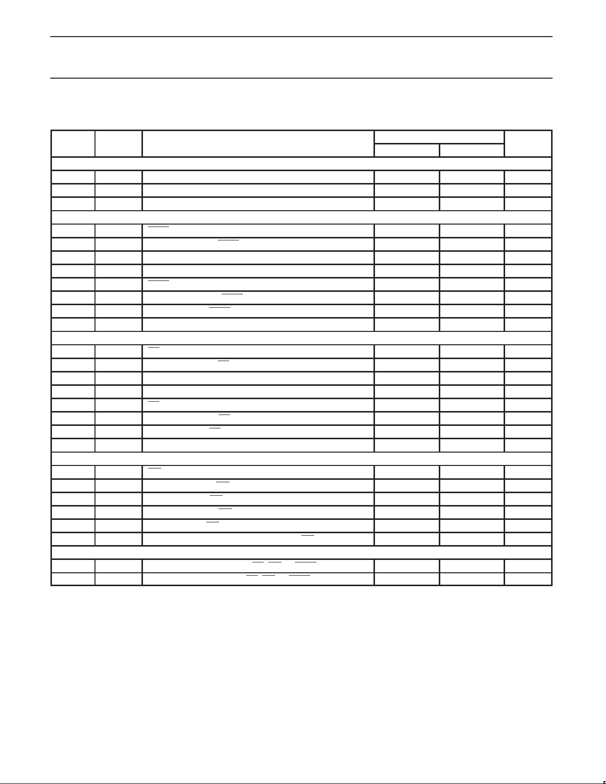
Philips Semiconductors Preliminary specification
SYMBOL
FIGURE
PARAMETER
UNIT
XA 16-bit microcontroller
32 K/1 K OTP/ROM/ROMless, 8-channel 8-bit A/D, low voltage (2.7 V–5.5 V),
2
C, 2 UARTs, 16 MB address range
I
AC ELECTRICAL CHARACTERISTICS (3 V)
VDD = 2.7 V to 4.5 V; T
Address Cycle
t
LHLL
t
AVLL
t
LLAX
26, 28, 30 ALE pulse width (programmable) (V1 * tC) – 10 ns
26, 28, 30 Address valid to ALE de-asserted (set-up) (V1 * tC) – 18 ns
26, 28, 30 Address hold after ALE de-asserted (tC/2) – 12 ns
Code Read Cycle
t
PLPH
t
LLPL
t
AVIVA
t
AVIVB
t
PLIV
t
PHIX
t
PHIZ
t
IXUA
Data Read Cycle
t
RLRH
t
LLRL
t
AVDVA
t
AVDVB
t
RLDV
t
RHDX
t
RHDZ
t
DXUA
Data Write Cycle
t
WLWH
t
LLWL
t
QVWX
t
WHQX
t
AVWL
t
UAWH
Wait Input
t
WTH
t
WTL
NOTES ON PAGE 41.
= 0 to +70°C for commercial, T
amb
= –40°C to +85°C for industrial.
amb
26 PSEN pulse width (V2 * tC) – 12 ns
26 ALE de-asserted to PSEN asserted (tC/2) – 9 ns
26 Address valid to instruction valid, ALE cycle (access time) (V3 * tC) – 58 ns
27 Address valid to instruction valid, non-ALE cycle (access time) (V4 * tC) – 52 ns
26 PSEN asserted to instruction valid (enable time) (V2 * tC) – 52 ns
26 Instruction hold after PSEN de-asserted 0 ns
26 Bus 3-State after PSEN de-asserted tC – 8 ns
26 Hold time of unlatched part of address after instruction latched 0 ns
28 RD pulse width (V7 * tC) – 12 ns
28 ALE de-asserted to RD asserted (tC/2) – 9 ns
28 Address valid to data input valid, ALE cycle (access time) (V6 * tC) – 58 ns
29 Address valid to data input valid, non-ALE cycle (access time) (V5 * tC) – 52 ns
28 RD low to valid data in (enable time) (V7 * tC) – 52 ns
28 Data hold time after RD de–asserted 0 ns
28 Bus 3-State after RD de-asserted (disable time) tC – 8 ns
28 Hold time of unlatched part of address after data latched 0 ns
30 WR pulse width (V8 * tC) – 12 ns
30 ALE falling edge to WR asserted (V12 * tC) – 10 ns
30 Data valid before WR asserted (data set-up time) (V13 * tC) – 28 ns
30 Data hold time after WR de-asserted (Note 6) (V11 * tC) – 8 ns
30 Address valid to WR asserted (address set-up time) (Note 5) (V9 * tC) – 28 ns
30 Hold time of unlatched part of address after WR is de-asserted (V11 * tC) – 10 ns
31 WAIT stable after bus strobe (RD, WR, or PSEN) asserted (V10 * tC) – 40 ns
31 WAIT hold after bus strobe (RD, WR, or PSEN) asserted (V10 * tC) – 5 ns
LIMITS
MIN MAX
XA-S3
2000 Aug 22
40
Page 41
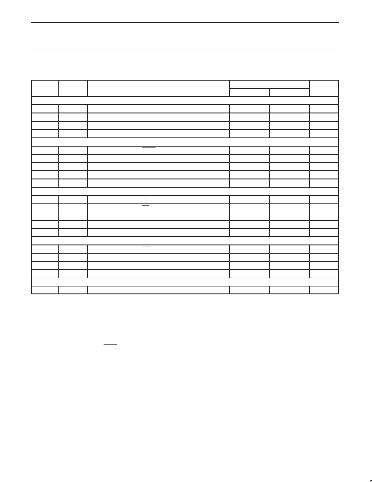
Philips Semiconductors Preliminary specification
SYMBOL
FIGURE
PARAMETER
UNIT
XA 16-bit microcontroller
32 K/1 K OTP/ROM/ROMless, 8-channel 8-bit A/D, low voltage (2.7 V–5.5 V),
2
C, 2 UARTs, 16 MB address range
I
AC ELECTRICAL CHARACTERISTICS (3 V RANGE) (continued)
This set of parameters is referenced to the XA-S3 clock output.
LIMITS
MIN MAX
Address Cycle
t
CHLH
t
CLLL
t
CHAV
t
CHAX
Code Read Cycle
t
CHPL
t
CHPH
t
IVCH
t
CHIX
t
CHIZ
Data Read Cycle
t
CHRL
t
CHRH
t
DVCH
t
CHDX
t
CHDZ
Data Write Cycle
t
CHWL
t
CHWH
t
QVCH
t
CHQX
Wait Input
t
CHWTH
NOTES:
1. Load capacitance for all outputs = 50 pF .
2. Variables V1 through V13 reflect programmable bus timing, which is programmed via the Bus T iming registers (BTRH and BTRL). R efer to
XA User Guide
the
V1) This variable represents the programmed width of the ALE pulse as determined by the ALEW bit in the BTRL register. V1 = 0.5 if the
V2) This variable represents the programmed width of the PSEN
V3) This variable represents the programmed length of an entire code read cycle with ALE. This time is determined by the CRA1 and
V4) This variable represents the programmed length of an entire code read cycle with no ALE. This time is determined by the CR1 and
V5) This variable represents the programmed length of an entire data read cycle with no ALE. This time is determined by the DR1 and
V6) This variable represents the programmed length of an entire data read cycle with ALE. The time is determined by the DRA1 and
26 CLKOUT rising edge to ALE rising edge – 15 ns
26 CLKOUT falling edge to ALE falling edge – 11 ns
26 CLKOUT rising edge to address valid – 29 ns
26 CLKOUT rising edge to address changing (hold time) 2 – ns
26 CLKOUT rising edge to PSEN asserted – 16 ns
26 CLKOUT rising edge to PSEN de-asserted – 15 ns
26 Instruction valid to CLKOUT rising edge (setup time) 30 – ns
26 CLKOUT rising edge to instruction changing (hold time) 0 – ns
26 CLKOUT rising edge to Bus 3-State (code read) – tC–8 ns
28 CLKOUT rising edge to RD asserted – 20 ns
28 CLKOUT rising edge to RD de-asserted – 16 ns
28 Data valid to CLKOUT rising edge (setup time) 28 – ns
28 CLKOUT rising edge to Data changing (hold time) 0 – ns
28 CLKOUT rising edge to Bus 3-State (data read) – tC–8 ns
30 CLKOUT falling edge to WR asserted – 19 ns
30 CLKOUT rising edge to WR de-asserted – 16 ns
30 Data valid to CLKOUT rising edge (setup time) 4 – ns
30 CLKOUT rising edge to Data changing (hold time) 0 – ns
31 WAIT valid prior to CLKOUT rising edge
8
30 4 ns
for details of the bus timing settings.
ALEW bit = 0, and 1.5 if the ALEW bit = 1.
pulse as determined by the CR1 and CR0 bits or the CRA1, CRA0, and
ALEW bits in the BTRL register.
– For a bus cycle with no ALE, V2 = 1 if CR1/0 = 00, 2 if CR1/0 = 01, 3 if CR1/0 = 10, and 4 if CR1/0 = 11. Note that during burst
mode code fetches, PSEN
does not exhibit transitions at the boundaries of bus cycles. V2 still applies for the purpose of
determining peripheral timing requirements.
– For a bus cycle with an ALE, V2 = the total bus cycle duration (2 if CRA1/0 = 00, 3 if CRA1/0 = 01, 4 if CRA1/0 = 10, and 5 if
CRA1/0 = 11) minus the number of clocks used by ALE (V1 + 0.5) = 2.
Example: if CRA1/0 = 10 and ALEW = 1, the V2 = 4 – (1.5 + 0.5) = 2.
CRA0 bits in the BTRL register. V3 = the total bus cycle duration (2 if CRA1/0 = 00, 3 if CRA1/0 = 01, 4 if CRA1/0 = 10, and
5 if CRA1/0 = 11).
CR0 bits in the BTRL register. V4 = 1 if CR1/0 = 00, 2 if CR1/0 = 01, 3 if CR1/0 = 10, and 4 if CR1/0 = 11.
DR0 bits in the BTRH register. V5 = 1 if DR1/0 = 00, 2 if DR1/0 = 01, 3 if DR1/0 = 10, and 4 if DR1/0 = 11.
DRA0 bits in the BTRH register. V6 = the total bus cycle duration (2 if DRA1/0 = 00, 3 if DRA1/0 = 01, 4 if DRA1/0 = 10, and
5 if DRA1/0 = 11).
XA-S3
2000 Aug 22
41
Page 42

Philips Semiconductors Preliminary specification
XA 16-bit microcontroller
32 K/1 K OTP/ROM/ROMless, 8-channel 8-bit A/D, low voltage (2.7 V–5.5 V),
2
C, 2 UARTs, 16 MB address range
I
XA-S3
V7) This variable represents the programmed width of the RD
BTRH register, and the SLEW bit in the BTRL register. Note that during a 16-bit operation on an 8-bit external bus, RD
and does not exhibit a transition between the first and second byte bus cycles. V7 still applies for the purpose of determining
peripheral timing requirements. The timing for the first byte is for a bus cycle with ALE, the timing for the second byte is for a bus
cycle with no ALE.
– For a bus cycle with no ALE, V7 = 1 if DR1/0 = 00, 2 if DR1/0 = 01, 3 if DR1/0 = 10, and 4 if DR1/0 = 11.
– For a bus cycle with an ALE, V7 = the total bus cycle duration (2 if DRA1/0 = 00, 3 if DRA1/0 = 01, 4 if DRA1/0 = 10, and
5 if DRA1/0 = 11) minus the number of clocks used by ALE (V1 + 0.5).
V8) This variable represents the programmed width of the WRL
V9) This variable represents the programmed address setup time for a write as determined by the data write cycle duration (defined by
V10) This variable represents the length of a bus strobe for calculation of WAIT set-up and hold times. The strobe may be RD
V11) This variable represents the programmed write hold time as determined by the WM0 bit in the BTRL register. V11 0 if the WM0 bit = 0,
V12) this variable represents the programmed period between the end of the ALE pulse and the beginning of the WRL
register, and the values of V1 and V8. V12 = the total bus cycle duration (2 if DWA1/0 = 00, 3 if DWA1/0 = 01, 4 if DWA1/0 = 10, and 5
V13) This variable represents the programmed data setup time for a write as determined by the data write cycle duration (defined by DW1
3. Not all combinations of bus timing configuration values result in valid bus cycles. Please refer to the
Bus for details.
4. When code is being fetched for execution on the external bus, a burst mode fetch is used that dows not have PSEN
cycle. This would be A3–A0 for an 8-bit bus, and A3–A1 for a 16-bit bus. Also, a 16-bit read operation conducted on an 8-bit wide bus
similarly does not include two separate RD
the second half of such a cycle.
5. This parameter is provided for peripherals that have the data clocked in on the falling edge of the WR strobe. This is not usually the case
and in most applications this parameter is not used.
6. Please note that the XA-S3 requires that extended data bus hold time (WM0 = 1) to be used with external bus write cycles.
7. Applies only to an external clock source, not when a crystal is connected to the XTAL1 and XTAL2 pins.
8. WAIT should not change between these times.
Example: if DRA1/0 = 00 and ALEW = 0, then V7 = 2 – (0.5 +0.5) = 1.
V8 = 1 if WM1 = 0, and 2 if WM1 = 1.
DW1 and DW0 or the DWA1 and DWA0 bits in the BTRH register), the WM0 bit in the BTRL register, and the value of V8.
– For a bus cycle with an ALE, V9 = the total bus write cycle duration (2 if DWA1/0 = 00, 3 if DWA1/0 = 01, 4 if DWA1/0 = 10, and
5 if DWA1/0 = 11) minus the number of clocks used by the WRL
hold time (0 if WM0 = 0 and 1 if WM0 = 1).
Example: If DWA1/0 = 10, WM0 = 1, and WM1 = 1, then V9 = 4 – 1 – 2 = 1.
– For a bus cycle with no ALE, V9 = the total bus cycle duration (2 if DW1/0 = 00, 3 if DW1/0 = 01, 4 if DW1/0 = 10, and
5 if DW1/0 = 11) minus the number of clocks used by the WRL
hold time (0 if WMo = 0 and 1 if WM0 = 1).
Example: If DW1/0 = 11, WM0 = 1, and WM1 = 0, then V9 = 5 – 1 – 1 = 3.
read cycles), WRL
widened by WAIT. V10 = 2 for WAIT associated with a code read cycle using PSEN
and/or WRH. V10 = V7 – 1 for a data read cycle using RD. This means that a single clock data read cycle cannot be stretched using
WAIT. If WAIT is used to vary the duration of data read cycles, the RD
Also see Note 4.
and 1 if the WM0 bit = 1.
as determined by the data write cycle duration (defined by the DWA1 and DWA0 bits in the BTRH register), the WM0 bit in the BTR L
if DWA1/0 = 11) minus the number of clocks used by the WRL
time (0 if WM0 = 0 and 1 if WM0 = 1), minus the width of the ALE pulse (V1).
Example: If SWA1/0 = 11, WM0 = 1, WM1 = 0, and ALEW = 1, then V12 = 5 – 1 – 1 – 1.5 = 1.5.
and DW0 or the DWA1 and DWA0 bits in the BTRH register), the WM0 bit in the BTRL register, and the values of V1 and V8.
– For a bus cycle with an ALE, V13 = the total bus cycle duration (2 if DWA1/0 = 00, 3 if DWA1/0 = 01, 4 if DWA1/0 = 10, and
5 if DWA1/0 = 11) minus the number of clocks used by the WRL
data hold time (0 if WM0 = 0 and 1 if WM0 = 1), minus the number of clocks used by ALE (V1 + 0.5).
Example: If DWA1/0 = 11, WM0 = 1, WM1 = 1, and ALEW = 0, then V13 = 5 – 1 – 2 – 1 = 1.
– For a bus cycle with no ALE, V13 = the total bus cycle duration (2 if DW1/0 = 00, 3 if DW1/0 = 01, 4 if DW1/0 = 10, and
5 if DW1/0 = 11) minus the number of clocks used by the WRL
data hold time (0 if WM0 = 0 and 1 if WM0 = 1).
Example: If DW1/0 = 01, WM0 = 1, and WM1 = 0, then V13 = 3 – 1 – 1 = 1.
and/or WRH (for data write cycles), or PSEN (for code read cycles), depending on the type of bus cycle being
strobes. So, a rising edge on the low order address line (A0) must be used to trigger a WAIT in
pulse as determined by the DR1 and DR0 bits or the DRA1, DRA0 in the
and/or WRH pulse as determined by the WM1 bit in the BTRL register.
and/or WRH pulse (V8) minus the number of clocks used by data
and/or WRH pulse (V8), minus the number of clocks used by data
. V10 = V8 for a data write cycle using WRL
strobe width must be set to be at least two clocks in duration.
and/or WRH pulse (V8), minus the number of clocks used by data hold
and/or WRH pulse (V8), minus the number of clocks used by
and/or WRH pulse (V8), minus the number of clocks used by
XA User Guide
section on the External
edges in every fetch
remains low
(for data
and/or WRH pulse
2000 Aug 22
42
Page 43
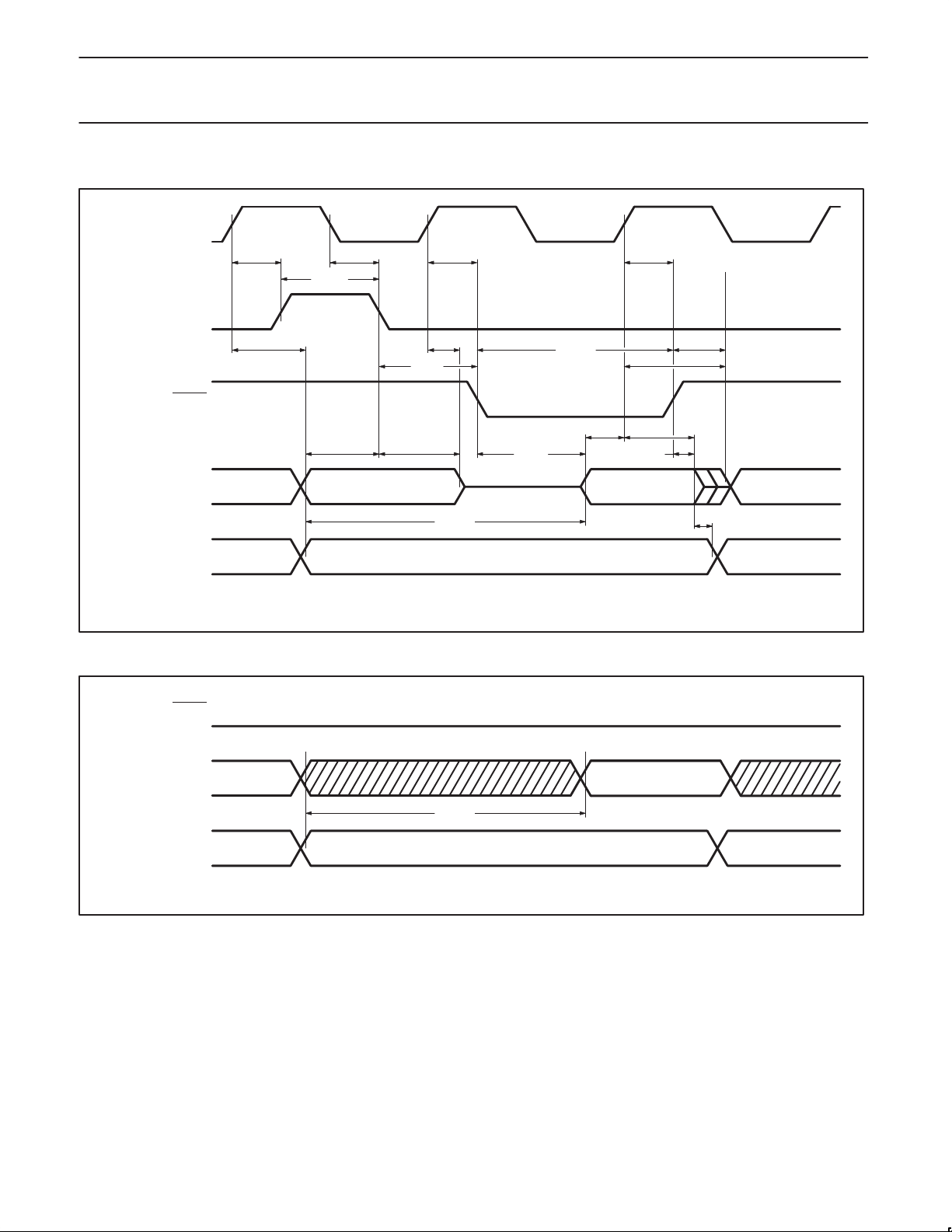
Philips Semiconductors Preliminary specification
XA 16-bit microcontroller
32 K/1 K OTP/ROM/ROMless, 8-channel 8-bit A/D, low voltage (2.7 V–5.5 V),
2
C, 2 UARTs, 16 MB address range
I
AC WAVEFORMS
CLKOUT
XA-S3
t
CHLH
t
LHLL
t
CLLL
t
CHPL
ALE
t
t
LLPL
CHAX
t
CHAV
PSEN
Multiplexed
Address and Data
Unmultiplexed
Address
t
AVLL
A4–A11 or A4–A23 INSTR IN*
t
LLAX
t
AVIVA
A0 or A1–A3, A12–A23
t
PLIV
*INSTR IN is either D0–D7 or D0–D15, depending on the bus width (8 or 16 bits).
Figure 26. External Program Memory Read Cycle (ALE Cycle)
t
PLPH
t
IVCH
t
CHPH
t
CHIX
t
PHIX
t
PHIZ
t
CHIZ
t
IXUA
SU00943A
PSEN
Multiplexed
Address and Data
t
AVIVB
Unmultiplexed
Address
A0 or A1–A3, A12–A23
*INSTR IN is either D0–D7 or D0–D15, depending on the bus width (8 or 16 bits).
Figure 27. External Program Memory Read Cycle (Non-ALE Cycle)
INSTR IN*
SU00949
2000 Aug 22
43
Page 44
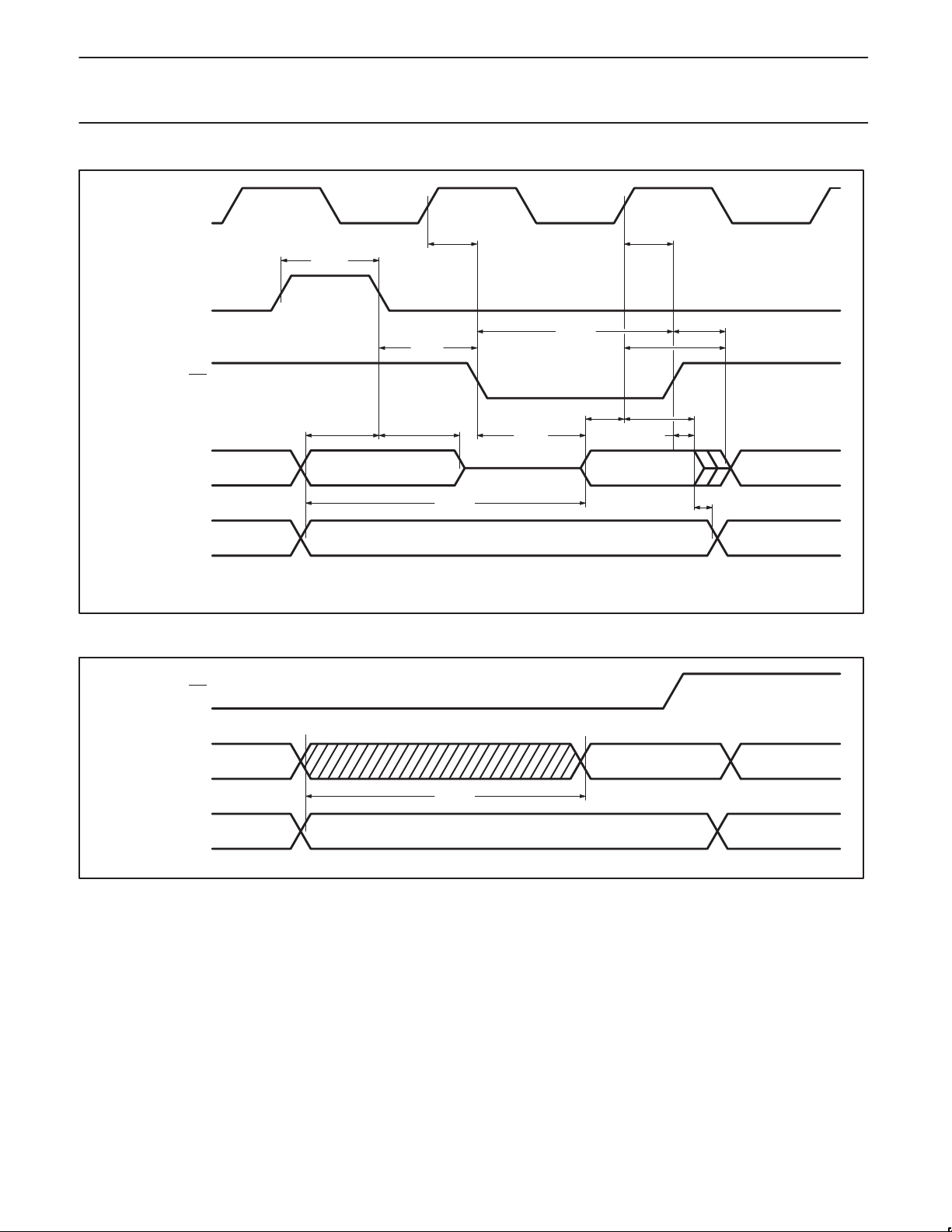
Philips Semiconductors Preliminary specification
XA 16-bit microcontroller
32 K/1 K OTP/ROM/ROMless, 8-channel 8-bit A/D, low voltage (2.7 V–5.5 V),
2
C, 2 UARTs, 16 MB address range
I
CLKOUT
XA-S3
t
CHRL
t
LHLL
ALE
t
LLRL
RD
Multiplexed
Address and Data
Unmultiplexed
Address
t
AVLL
A4–A11 or A4–A23 DATA IN*
t
LLAX
t
AVDVA
A0 or A1–A3, A12–A23
t
RLDV
*DATA IN is either D0–D7 or D0–D15, depending on the bus width (8 or 16 bits).
Figure 28. External Data Memory Read Cycle (ALE Cycle)
t
RLRH
t
DVCH
t
CHRH
t
CHDX
t
RHDX
t
RHDZ
t
CHDZ
t
DXUA
SU00944
RD
Multiplexed
Address and Data
Unmultiplexed
Address
D0–D7
t
AVDVB
A0–A3, A12–A23
Figure 29. External Data Memory Read Cycle (Non-ALE Cycle)
SU00950A
2000 Aug 22
44
Page 45
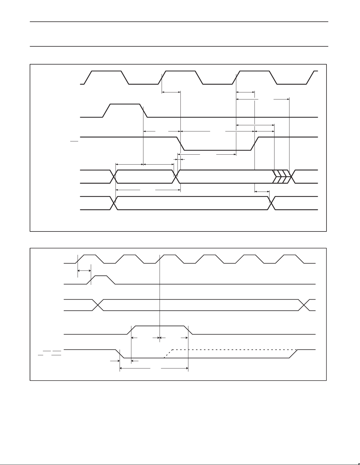
Philips Semiconductors Preliminary specification
XA 16-bit microcontroller
32 K/1 K OTP/ROM/ROMless, 8-channel 8-bit A/D, low voltage (2.7 V–5.5 V),
2
C, 2 UARTs, 16 MB address range
I
CLKOUT
XA-S3
t
CHWL
ALE
t
LLWL
WR
t
QVWX
Multiplexed
Address and Data
Unmultiplexed
Address
t
AVLL
t
LLAX
A4–A11 or A4–A23 DA TA OUT*
t
AVWL
A0 or A1–A3, A12–A23
*DATA OUT is either D0–D7 or D0–D15, depending on the bus width (8 or 16 bits).
Figure 30. External Data Memory Write Cycle
XTAL1
t
CRAR
t
QVCH
t
WLWH
t
CHWH
t
CHQZ
t
CHQX
t
WHQX
t
UAWH
SU00945
ALE
ADDRESS BUS
WAIT
BUS STROBE
(WRL, WRH,
RD, OR PSEN)
t
WTH
t
CHWTH
t
CHWTL
t
WTL
Figure 31. WAIT Signal Timing
(The dashed line shows the strobe without WAIT.)
SU01068
2000 Aug 22
45
Page 46
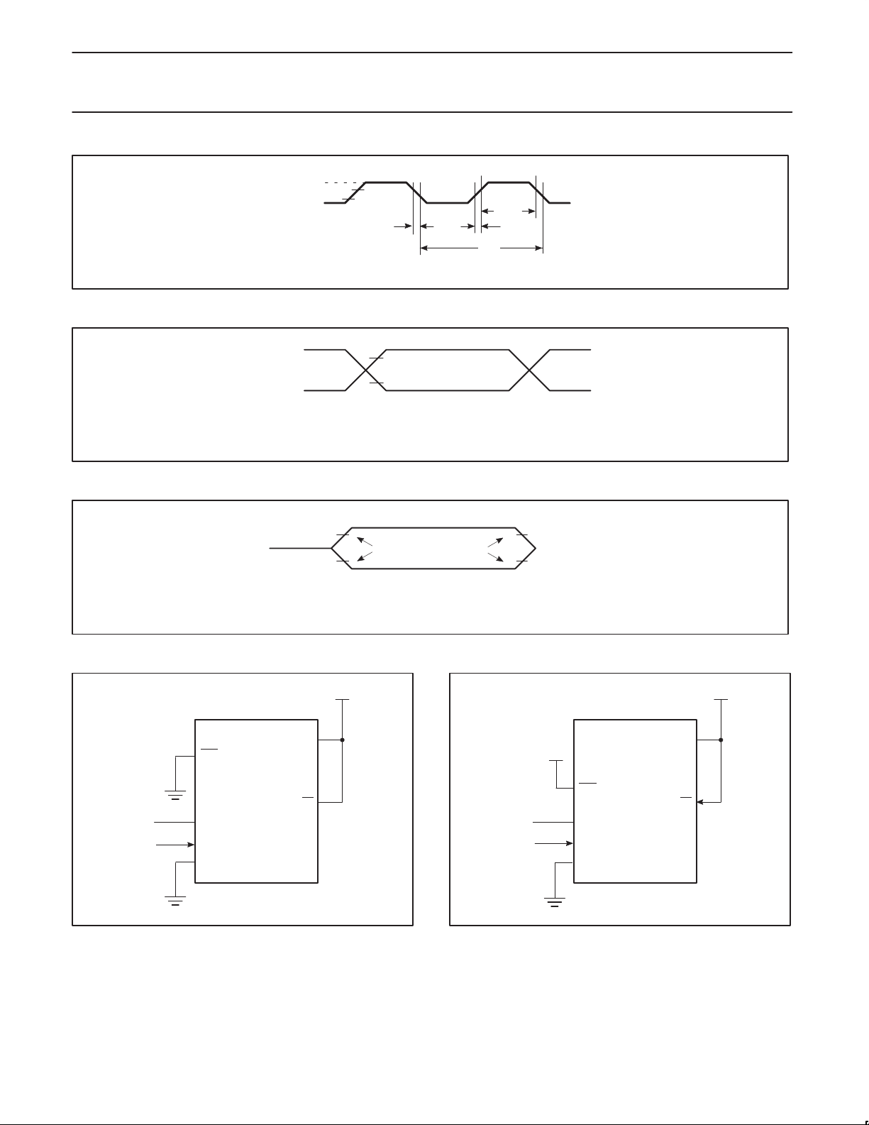
Philips Semiconductors Preliminary specification
XA 16-bit microcontroller
32 K/1 K OTP/ROM/ROMless, 8-channel 8-bit A/D, low voltage (2.7 V–5.5 V),
2
C, 2 UARTs, 16 MB address range
I
XA-S3
VDD–0.5
0.45V
0.7V
DD
0.2VDD–0.1
t
CHCL
t
CLCX
t
C
t
CHCX
t
CLCH
SU00842
Figure 32. External Clock Drive
VDD–0.5
0.45V
NOTE:
AC inputs during testing are driven at VDD –0.5 for a logic ‘1’ and 0.45V for a logic ‘0’.
Timing measurements are made at the 50% point of transitions.
0.2V
0.2V
+0.9
DD
–0.1
DD
SU00703A
Figure 33. AC Testing Input/Output
V
+0.1V
LOAD
LOAD
V
LOAD
–0.1V
V
NOTE:
For timing purposes, a port is no longer floating when a 100mV change from load voltage occurs,
and begins to float when a 100mV change from the loaded V
TIMING
REFERENCE
POINTS
level occurs. IOH/IOL ≥ ±20mA.
OH/VOL
–0.1V
V
OH
V
+0.1V
OL
SU00011
Figure 34. Float Waveform
CLOCK SIGNAL
2000 Aug 22
V
DD
V
DD
EA
SU00591B
(NC)
RST
XTAL2
XTAL1
V
SS
Figure 35. IDD Test Condition, Active Mode
All other pins are disconnected
46
(NC)
CLOCK SIGNAL
Figure 36. IDD Test Condition, Idle Mode
V
V
DD
RST
XTAL2
XTAL1
V
SS
DD
EA
SU00590B
All other pins are disconnected
V
DD
Page 47
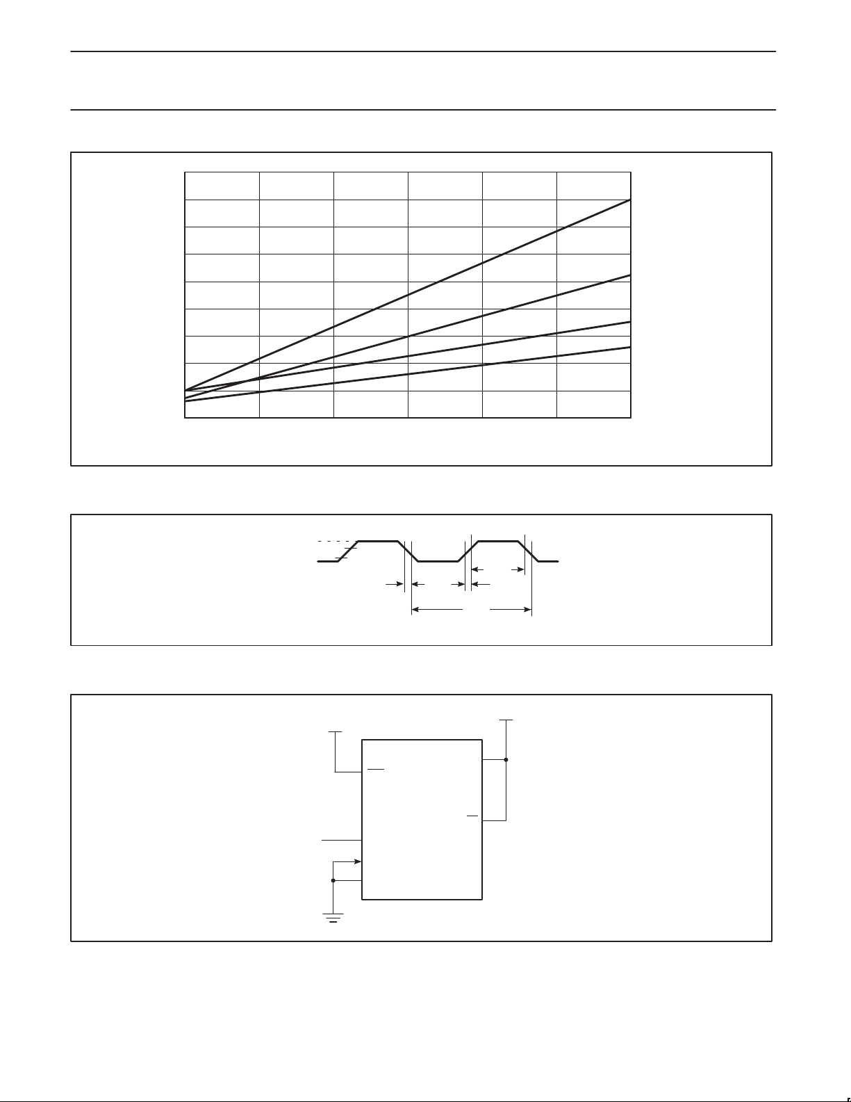
Philips Semiconductors Preliminary specification
XA 16-bit microcontroller
32 K/1 K OTP/ROM/ROMless, 8-channel 8-bit A/D, low voltage (2.7 V–5.5 V),
2
C, 2 UARTs, 16 MB address range
I
90
XA-S3
80
70
60
50
mA
40
30
20
10
0
0 5 10 15 20 25 30
Frequency (MHz)
Figure 37. IDD vs. Frequency
Valid only within frequency specification of the device under test.
VDD–0.5
0.45V
0.7V
DD
0.2VDD–0.1
t
CHCL
t
CLCX
t
CHCX
t
CLCH
t
CL
Max. IDD (Active)
DD
DD
(Idle)
(Idle)
DD
(Active)
Typical I
Max. I
Typical I
SU01228
SU00608A
Figure 38. Clock Signal Waveform for IDD Tests in Active and Idle Modes
t
(NC)
= t
CLCH
V
DD
RST
XTAL2
XTAL1
V
SS
CHCL
= 5 ns
V
DD
EA
SU00585A
V
DD
Figure 39. IDD Test Condition, Power Down Mode
All other pins are disconnected. V
=2 V to 5.5 V
DD
2000 Aug 22
47
Page 48
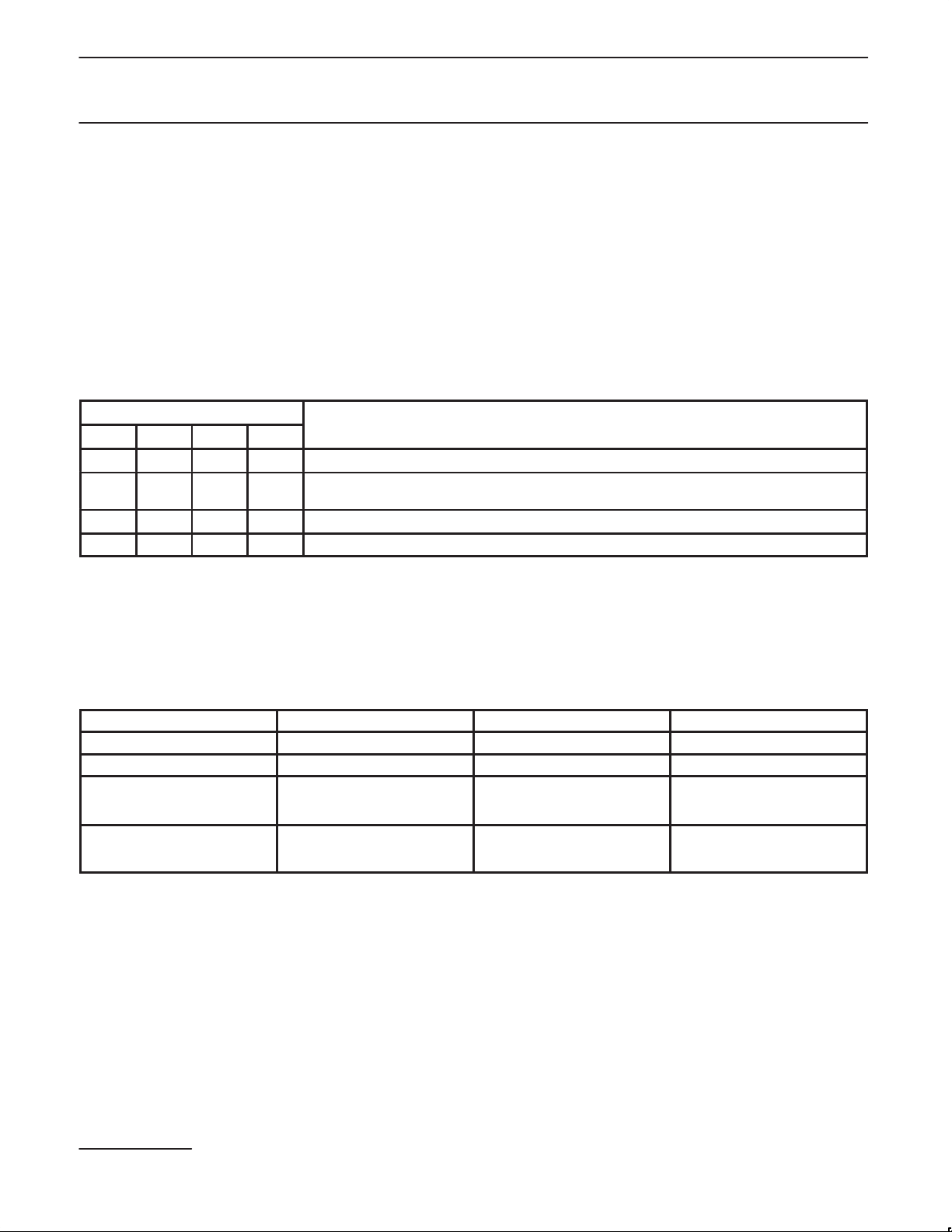
Philips Semiconductors Preliminary specification
XA 16-bit microcontroller
32 K/1 K OTP/ROM/ROMless, 8-channel 8-bit A/D, low voltage (2.7 V–5.5 V),
2
C, 2 UARTs, 16 MB address range
I
XA-S3
EPROM CHARACTERISTICS
The XA-S3 is programmed by using a modified Improved
Quick-Pulse Programming algorithm. This algorithm is essentially
the same as that used by 80C51 family EPROM parts. However
different pins are used for many programming functions.
Detailed EPROM programming information may be obtained from
the Internet at www.philipsmcu.com/ftp.html.
The XA-S3 contains three signature bytes that can be read and
used by an EPROM programming system to identify the device. The
signature bytes identify the device as an XA-S3 manufactured by
Philips.
Security Bits
With none of the security bits programmed the code in the program
memory can be verified. When only security bit 1 is programmed,
MOVC instructions executed from external program memory are
disabled from fetching code bytes from the internal memory. All
further programming of the EPROM is disabled. When security bits
1 and 2 are programmed, in addition to the above, verify mode is
disabled. When all three security bits are programmed, all of the
conditions above apply and all external program memory execution
is disabled. (See Table 6.)
Table 6. Program Security Bits
PROGRAM LOCK BITS
SB1 SB2 SB3 PROTECTION DESCRIPTION
1 U U U No Program Security features enabled.
2 P U U MOVC instructions executed from external program memory are disabled from fetching code bytes
3 P P U Same as 2, also verify is disabled.
4 P P P Same as 3, external execution is disabled. Internal data RAM is not accessible.
NOTES:
1. P – programmed. U – unprogrammed.
2. Any other combination of the security bits is not defined.
from internal memory and further programming of the EPROM is disabled.
ROM CODE SUBMISSION
When submitting ROM code for the XA-S3, the following must be specified:
1. 32k byte user ROM data
2. ROM security bits.
ADDRESS
0000H to 7FFFH DATA 7:0 User ROM Data
8020H SEC 0 ROM Security Bit 1
8020H SEC 1 ROM Security Bit 2
8020H SEC 3 ROM Security Bit 3
CONTENT BIT(S) COMMENT
0 = enable security
1 = disable security
0 = enable security
1 = disable security
Trademark phrase of Intel Corporation.
2000 Aug 22
48
Page 49
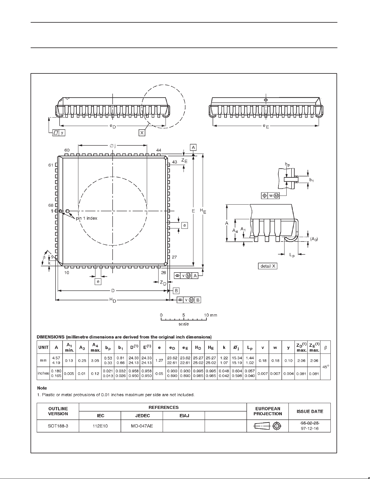
Philips Semiconductors Preliminary specification
XA 16-bit microcontroller
32 K/1 K OTP/ROM/ROMless, 8-channel 8-bit A/D, low voltage (2.7 V–5.5 V),
2
C, 2 UARTs, 16 MB address range
I
PLCC68: plastic leaded chip carrier; 68 leads; pedestal SOT188-3
XA-S3
2000 Aug 22
49
Page 50
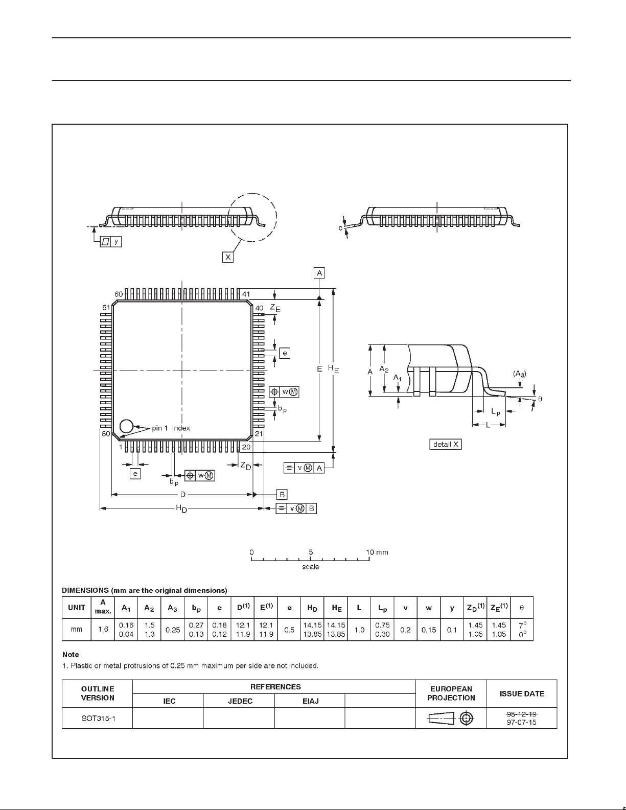
Philips Semiconductors Preliminary specification
XA 16-bit microcontroller
32 K/1 K OTP/ROM/ROMless, 8-channel 8-bit A/D, low voltage (2.7 V–5.5 V),
2
C, 2 UARTs, 16 MB address range
I
LQFP80: plastic low profile quad flat package; 80 leads; body 12 x 12 x 1.4 mm SOT315-1
XA-S3
2000 Aug 22
50
Page 51

Philips Semiconductors Preliminary specification
XA 16-bit microcontroller
32 K/1 K OTP/ROM/ROMless, 8-channel 8-bit A/D, low voltage (2.7 V–5.5 V),
2
C, 2 UARTs, 16 MB address range
I
NOTES
XA-S3
2000 Aug 22
51
Page 52

Philips Semiconductors Preliminary specification
XA 16-bit microcontroller
32 K/1 K OTP/ROM/ROMless, 8-channel 8-bit A/D, low voltage (2.7 V–5.5 V),
2
C, 2 UARTs, 16 MB address range
I
Data sheet status
Data sheet
status
Objective
specification
Preliminary
specification
Product
specification
Product
status
Development
Qualification
Production
Definition
This data sheet contains the design target or goal specifications for product development.
Specification may change in any manner without notice.
This data sheet contains preliminary data, and supplementary data will be published at a later date.
Philips Semiconductors reserves the right to make changes at any time without notice in order to
improve design and supply the best possible product.
This data sheet contains final specifications. Philips Semiconductors reserves the right to make
changes at any time without notice in order to improve design and supply the best possible product.
[1]
XA-S3
[1] Please consult the most recently issued datasheet before initiating or completing a design.
Definitions
Short-form specification — The data in a short-form specification is extracted from a full data sheet with the same type number and title. For
detailed information see the relevant data sheet or data handbook.
Limiting values definition — Limiting values given are in accordance with the Absolute Maximum Rating System (IEC 134). Stress above one
or more of the limiting values may cause permanent damage to the device. These are stress ratings only and operation of the device at these or
at any other conditions above those given in the Characteristics sections of the specification is not implied. Exposure to limiting values for extended
periods may affect device reliability.
Application information — Applications that are described herein for any of these products are for illustrative purposes only. Philips
Semiconductors make no representation or warranty that such applications will be suitable for the specified use without further testing or
modification.
Disclaimers
Life support — These products are not designed for use in life support appliances, devices or systems where malfunction of these products can
reasonably be expected to result in personal injury . Philips Semiconductors customers using or selling these products for use in such applications
do so at their own risk and agree to fully indemnify Philips Semiconductors for any damages resulting from such application.
Right to make changes — Philips Semiconductors reserves the right to make changes, without notice, in the products, including circuits, standard
cells, and/or software, described or contained herein in order to improve design and/or performance. Philips Semiconductors assumes no
responsibility or liability for the use of any of these products, conveys no license or title under any patent, copyright, or mask work right to these
products, and makes no representations or warranties that these products are free from patent, copyright, or mask work right infringement, unless
otherwise specified.
Philips Semiconductors
811 East Arques Avenue
P.O. Box 3409
Sunnyvale, California 94088–3409
Telephone 800-234-7381
Copyright Philips Electronics North America Corporation 2000
All rights reserved. Printed in U.S.A.
Date of release: 08-00
Document order number: 9397 750 07444
2000 Aug 22
52
 Loading...