

Page 1

INTEGRATED CIRCUITS
XA-G3
XA 16-bit microcontroller family
32K/512 OTP/ROM/ROMless, watchdog, 2 UARTs
Product specification
Supersedes data of 1998 Aug 14
IC25 Data Handbook
1999 Apr 07
Page 2
Philips Semiconductors Product specification
XA 16-bit microcontroller family
32K/512 OTP/ROM/ROMless, watchdog, 2 UARTs
FAMILY DESCRIPTION
The Philips Semiconductors XA (eXtended Architecture) family of
16-bit single-chip microcontrollers is powerful enough to easily
handle the requirements of high performance embedded
applications, yet inexpensive enough to compete in the market for
high-volume, low-cost applications.
The XA family provides an upward compatibility path for 80C51
users who need higher performance and 64k or more of program
memory. Existing 80C51 code can also easily be translated to run
on XA microcontrollers.
The performance of the XA architecture supports the
comprehensive bit-oriented operations of the 80C51 while
incorporating support for multi-tasking operating systems and
high-level languages such as C. The speed of the XA architecture,
at 10 to 100 times that of the 80C51, gives designers an easy path
to truly high performance embedded control.
The XA architecture supports:
•Upward compatibility with the 80C51 architecture
•16-bit fully static CPU with a 24-bit program and data address
range
•Eight 16-bit CPU registers each capable of performing all
arithmetic and logic operations as well as acting as memory
pointers. Operations may also be performed directly to memory.
•Both 8-bit and 16-bit CPU registers, each capable of performing
all arithmetic and logic operations.
•An enhanced instruction set that includes bit intensive logic
operations and fast signed or unsigned 16 × 16 multiply and
32 / 16 divide
XA-G3
•Instruction set tailored for high level language support
•Multi-tasking and real-time executives that include up to 32
vectored interrupts, 16 software traps, segmented data memory,
and banked registers to support context switching
•Low power operation, which is intrinsic to the XA architecture,
includes power-down and idle modes.
More detailed information on the core is available in the XA User
Guide.
SPECIFIC FEATURES OF THE XA-G3
•20-bit address range, 1 megabyte each program and data space.
(Note that the XA architecture supports up to 24 bit addresses.)
•2.7V to 5.5V operation
•32K bytes on-chip EPROM/ROM program memory =
XA-G37/XA-G33
•512 bytes of on-chip data RAM
•Three counter/timers with enhanced features
(equivalent to 80C51 T0, T1, and T2)
•Watchdog timer
•Two enhanced UARTs
•Four 8-bit I/O ports with 4 programmable output configurations
•44-pin PLCC and 44-pin LQFP packages
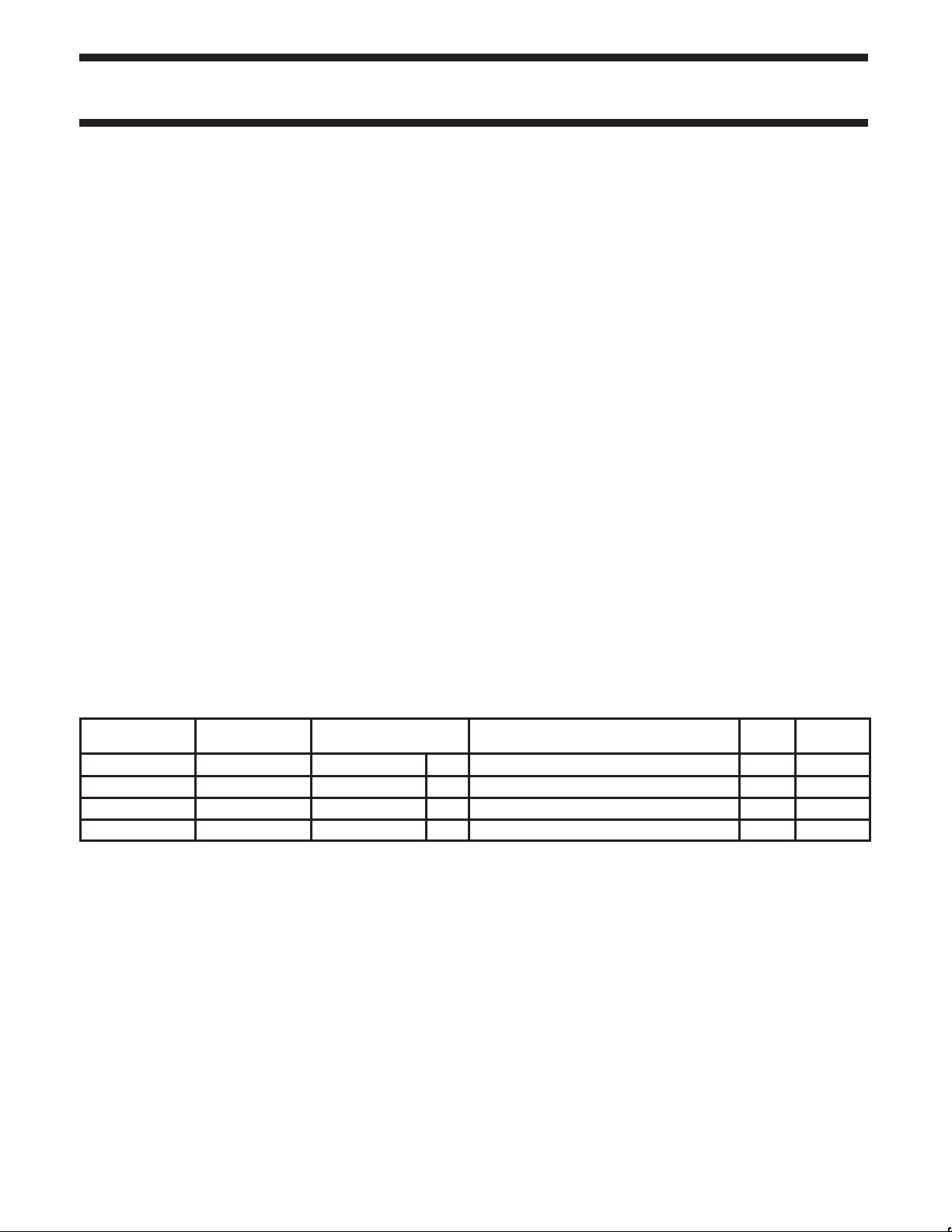
ORDERING INFORMATION
ROMless ROM EPROM
P51XAG30KB BD P51XAG33KB BD PXAG37KB BD OTP 0 to +70, Plastic Low Profile Quad Flat Pkg. 30 SOT389–1
P51XAG30KB A P51XAG33KB A PXAG37KB A OTP 0 to +70, Plastic Leaded Chip Carrier 30 SOT187–2
P51XAG30KF BD P51XAG33KF BD PXAG37KF BD OTP –40 to +85, Plastic Low Profile Quad Flat Pkg. 30 SOT389–1
P51XAG30KF A P51XAG33KF A PXAG37KF A OTP –40 to +85, Plastic Leaded Chip Carrier 30 SOT187–2
NOTE:
1. OTP = One Time Programmable EPROM. UV = Erasable EPROM.
1
TEMPERATURE RANGE °C AND PACKAGE
FREQ
(MHz)
DRAWING
NUMBER
1999 Apr 07 853-2052 21197
2
Page 3

Philips Semiconductors Product specification
XA 16-bit microcontroller family
32K/512 OTP/ROM/ROMless, watchdog, 2 UARTs
PIN CONFIGURATIONS
44-Pin PLCC Package
6140
7
17
Pin Function
1V
SS
2 P1.0/A0/WRH
3 P1.1/A1
4 P1.2/A2
5 P1.3/A3
6 P1.4/RxD1
7 P1.5/TxD1
8 P1.6/T2
9 P1.7/T2EX
10 RST
11 P3.0/RxD0
12 NC
13 P3.1/TxD0
14 P3.2/INT0
15 P3.3/INT1
16 P3.4/T0
17 P3.5/T1/BUSW
18 P3.6/WR
19 P3.7/RD
20 XTAL2
21 XTAL1
22 V
L
SS
PLCC
18 28
Pin Function
23 V
24 P2.0/A12D8
25 P2.1/A13D9
26 P2.2/A14D10
27 P2.3/A15D11
28 P2.4/A16D12
29 P2.5/A17D13
30 P2.6/A18D14
31 P2.7/A19D15
32 PSEN
33 ALE/PROG
34 NC
35 EA
36 P0.7/A11D7
37 P0.6/A10D6
38 P0.5/A9D5
39 P0.4/A8D4
40 P0.3/A7D3
41 P0.2/A6D2
42 P0.1/A5D1
43 P0.0/A4D0
44 V
39
29
DD
/VPP/WAIT
DD
SU00525
44-Pin LQFP Package
44 34
1
11
12 22
Pin Function
1 P1.5/TxD1
2 P1.6/T2
3 P1.7/T2EX
4 RST
5 P3.0/RxD0
6NC
7 P3.1/TxD0
8 P3.2/INT0
9 P3.3/INT1
10 P3.4/T0
11 P3.5/T1/BUSW
12 P3.6/WRL
13 P3.7/RD
14 XTAL2
15 XTAL1
16 V
SS
17 V
DD
18 P2.0/A12D8
19 P2.1/A13D9
20 P2.2/A14D10
21 P2.3/A15D11
22 P2.4/A16/D12
LQFP
Pin Function
23 P2.5/A17D13
24 P2.6/A18D14
25 P2.7/A19D15
26 PSEN
27 ALE/PROG
28 NC
29 EA
30 P0.7/A11D7
31 P0.6/A10D6
32 P0.5/A9D5
33 P0.4/A8D4
34 P0.3/A7D3
35 P0.2/A6D2
36 P0.1/A5D1
37 P0.0/A4D0
38 V
39 V
40 P1.0/A0/WRH
41 P1.1/A1
42 P1.2/A2
43 P1.3/A3
44 P1.4/RxD1
/VPP/WAIT
DD
SS
SU00580
XA-G3
33
23
LOGIC SYMBOL
* NOT AVAILABLE ON 40-PIN DIP PACKAGE
RxD0
TxD0
INT0
INT1
T0
T1/BUSW
WRL
ALTERNATE FUNCTIONS
RD
RST
EA/WAIT
PSEN
ALE
VDDV
SS
XTAL1
XTAL2
PORT 3
PORT 1PORT 2
PORT 0
ADDRESS AND DATA BUS
T2EX*
T2*
TXD1
D1
R
X
A3
A2
A1
A0/WRH
BUS
ADDRESS
SU00526
1999 Apr 07
3
Page 4
Philips Semiconductors Product specification
XA 16-bit microcontroller family
32K/512 OTP/ROM/ROMless, watchdog, 2 UARTs
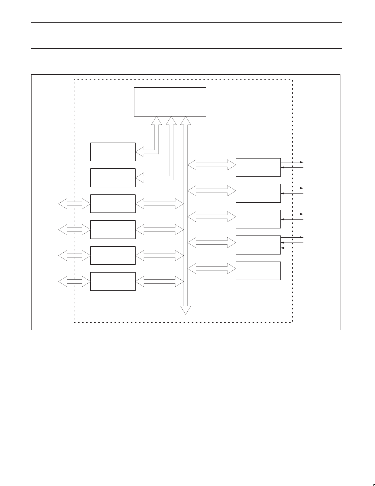
BLOCK DIAGRAM
XA CPU Core
Program
Memory
Bus
32K BYTES
ROM/EPROM
512 BYTES
STATIC RAM
PORT 0
Data Bus
XA-G3
SFR BUS
UART0
UART1
PORT 1
PORT 2
PORT 3
TIMER 0 &
TIMER 1
TIMER 2
WATCHDOG
TIMER
SU00527
1999 Apr 07
4
Page 5

Philips Semiconductors Product specification
MNEMONIC
TYPE
NAME AND FUNCTION
XA 16-bit microcontroller family
XA-G3
32K/512 OTP/ROM/ROMless, watchdog, 2 UARTs
PIN DESCRIPTIONS
PIN. NO.
PLCC LQFP
V
SS
V
DD
P0.0 – P0.7 43–36 37–30 I/O Port 0: Port 0 is an 8-bit I/O port with a user-configurable output type. Port 0 latches have 1s
P1.0 – P1.7 2–9 40–44,
P2.0 – P2.7 24–31 18–25 I/O Port 2: Port 2 is an 8-bit I/O port with a user-configurable output type. Port 2 latches have 1s
P3.0 – P3.7 11,
RST 10 4 I Reset: A low on this pin resets the microcontroller, causing I/O ports and peripherals to take on
ALE/PROG 33 27 I/O Address Latch Enable/Program Pulse: A high output on the ALE pin signals external circuitry to
1, 22 16 I Ground: 0V reference.
23, 44 17 I Power Supply: This is the power supply voltage for normal, idle, and power down operation.
written to them and are configured in the quasi-bidirectional mode during reset. The operation of
port 0 pins as inputs and outputs depends upon the port configuration selected. Each port pin is
configured independently. Refer to the section on I/O port configuration and the DC Electrical
Characteristics for details.
When the external program/data bus is used, Port 0 becomes the multiplexed low data/instruction
byte and address lines 4 through 11.
1–3
2 40 O A0/WRH: Address bit 0 of the external address bus when the external data bus is
3 41 O A1: Address bit 1 of the external address bus.
4 42 O A2: Address bit 2 of the external address bus.
5 43 O A3: Address bit 3 of the external address bus.
6 44 I RxD1 (P1.4): Receiver input for serial port 1.
7 1 O TxD1 (P1.5): Transmitter output for serial port 1.
8 2 I/O T2 (P1.6): T imer/counter 2 external count input/clockout.
9 3 I T2EX (P1.7): Timer/counter 2 reload/capture/direction control
13–195,7–13
11 5 I RxD0 (P3.0): Receiver input for serial port 0.
13 7 O TxD0 (P3.1): Transmitter output for serial port 0.
14 8 I INT0 (P3.2): External interrupt 0 input.
15 9 I INT1 (P3.3): External interrupt 1 input.
16 10 I/O T0 (P3.4): Timer 0 external input, or timer 0 overflow output.
17 11 I/O T1/BUSW (P3.5): Timer 1 external input, or timer 1 overflow output. The value on this pin is
18 12 O WRL (P3.6): External data memory low byte write strobe.
19 13 O RD (P3.7): External data memory read strobe.
I/O Port 1: Port 1 is an 8-bit I/O port with a user-configurable output type. Port 1 latches have 1s
written to them and are configured in the quasi-bidirectional mode during reset. The operation of
port 1 pins as inputs and outputs depends upon the port configuration selected. Each port pin is
configured independently. Refer to the section on I/O port configuration and the DC Electrical
Characteristics for details.
Port 1 also provides special functions as described below.
configured for an 8 bit width. When the external data bus is configured for a 16
bit width, this pin becomes the high byte write strobe.
written to them and are configured in the quasi-bidirectional mode during reset. The operation of
port 2 pins as inputs and outputs depends upon the port configuration selected. Each port pin is
configured independently. Refer to the section on I/O port configuration and the DC Electrical
Characteristics for details.
When the external program/data bus is used in 16-bit mode, Port 2 becomes the multiplexed high
data/instruction byte and address lines 12 through 19. When the external program/data bus is used in
8-bit mode, the number of address lines that appear on port 2 is user programmable.
I/O Port 3: Port 3 is an 8-bit I/O port with a user configurable output type. Port 3 latches have 1s
written to them and are configured in the quasi-bidirectional mode during reset. the operation of
port 3 pins as inputs and outputs depends upon the port configuration selected. Each port pin is
configured independently. Refer to the section on I/O port configuration and the DC Electrical
Characteristics for details.
Port 3 also provides various special functions as described below.
latched as the external reset input is released and defines the default
external data bus width (BUSW). 0 = 8-bit bus and 1 = 16-bit bus.
their default states, and the processor to begin execution at the address contained in the reset
vector. Refer to the section on Reset for details.
latch the address portion of the multiplexed address/data bus. A pulse on ALE occurs only when it
is needed in order to process a bus cycle.
1999 Apr 07
5
Page 6

Philips Semiconductors Product specification
SFR
NAME
DESCRIPTION
SFR
XA 16-bit microcontroller family
XA-G3
32K/512 OTP/ROM/ROMless, watchdog, 2 UARTs
MNEMONIC NAME AND FUNCTIONTYPE
MNEMONIC NAME AND FUNCTIONTYPE
PSEN 32 26 O Program Store Enable: The read strobe for external program memory. When the microcontroller
EA/WAIT/
V
PP
XTAL1 21 15 I Crystal 1: Input to the inverting amplifier used in the oscillator circuit and input to the internal clock
XTAL2 20 14 O Crystal 2: Output from the oscillator amplifier.
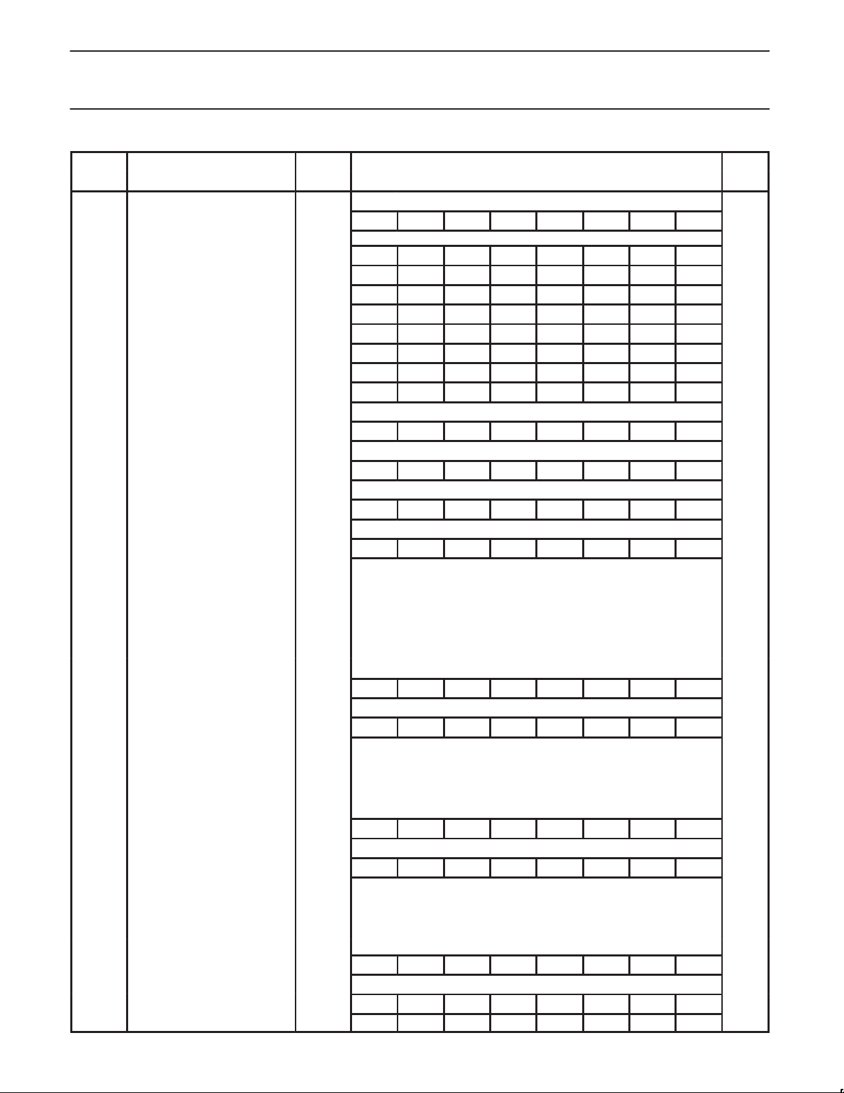
SPECIAL FUNCTION REGISTERS
PIN. NO.
LQFPPLCC
accesses external program memory, PSEN
is only active when external code accesses are performed.
35 29 I External Access/Wait: The EA input determines whether the internal program memory of the
microcontroller is used for code execution. The value on the EA pin is latched as the external reset
input is released and applies during later execution. When latched as a 0, external program
memory is used exclusively, when latched as a 1, internal program memory will be used up to its
limit, and external program memory used above that point. After reset is released, this pin takes on
the function of bus Wait input. If Wait is asserted high during any external bus access, that cycle
will be extended until Wait is released. During EPROM programming, this pin is also the
programming supply voltage input.
generator circuits.
BIT FUNCTIONS AND ADDRESSES
ADDRESS
MSB LSB
is driven low in order to enable memory devices. PSEN
RESET
VALUE
BCR Bus configuration register 46A — — — WAITD BUSD BC2 BC1 BC0 Note 1
BTRH Bus timing register high byte 469 DW1 DW0 DWA1 DWA0 DR1 DR0 DRA1 DRA0 FF
BTRL Bus timing register low byte 468 WM1 WM0 ALEW — CR1 CR0 CRA1 CRA0 EF
CS Code segment 443 00
DS Data segment 441 00
ES Extra segment 442 00
33F 33E 33D 33C 33B 33A 339 338
IEH* Interrupt enable high byte 427 — — — — ETI1 ERI1 ETI0 ERI0 00
337 336 335 334 333 332 331 330
IEL* Interrupt enable low byte 426 EA — — ET2 ET1 EX1 ET0 EX0 00
IPA0 Interrupt priority 0 4A0 — PT0 — PX0 00
IPA1 Interrupt priority 1 4A1 — PT1 — PX1 00
IPA2 Interrupt priority 2 4A2 — — — PT2 00
IPA4 Interrupt priority 4 4A4 — PTI0 — PRI0 00
IPA5 Interrupt priority 5 4A5 — PTI1 — PRI1 00
387 386 385 384 383 382 381 380
P0* Port 0 430 AD7 AD6 AD5 AD4 AD3 AD2 AD1 AD0 FF
38F 38E 38D 38C 38B 38A 389 388
P1* Port 1 431 T2EX T2 TxD1 RxD1 A3 A2 A1 WRH FF
397 396 395 394 393 392 391 390
P2* Port 2 432 P2.7 P2.6 P2.5 P2.4 P2.3 P2.2 P2.1 P2.0 FF
1999 Apr 07
6
Page 7
Philips Semiconductors Product specification
XA 16-bit microcontroller family
XA-G3
32K/512 OTP/ROM/ROMless, watchdog, 2 UARTs
SFR
NAME
NAME
P3* Port 3 433 RD WR T1 T0 INT1 INT0 TxD0 RxD0 FF
P0CFGA Port 0 configuration A 470 Note 5
P1CFGA Port 1 configuration A 471 Note 5
P2CFGA Port 2 configuration A 472 Note 5
P3CFGA Port 3 configuration A 473 Note 5
P0CFGB Port 0 configuration B 4F0 Note 5
P1CFGB Port 1 configuration B 4F1 Note 5
P2CFGB Port 2 configuration B 4F2 Note 5
P3CFGB Port 3 configuration B 4F3 Note 5
PCON* Power control register 404 — — — — — — PD IDL 00
PSWH* Program status word (high byte) 401 SM TM RS1 RS0 IM3 IM2 IM1 IM0 Note 2
PSWL* Program status word (low byte) 400 C AC — — — V N Z Note 2
PSW51* 80C51 compatible PSW 402 C AC F0 RS1 RS0 V F1 P Note 3
DESCRIPTION
DESCRIPTION
SFR
ADDRESS
ADDRESS
39F 39E 39D 39C 39B 39A 399 398
227 226 225 224 223 222 221 220
20F 20E 20D 20C 20B 20A 209 208
207 206 205 204 203 202 201 200
217 216 215 214 213 212 211 210
BIT FUNCTIONS AND ADDRESSES
RESET
RESET
VALUE
VALUE
LSBMSB
RTH0 Timer 0 extended reload,
high byte
RTH1 Timer 1 extended reload,
high byte
RTL0 Timer 0 extended reload, low byte 454 00
RTL1 Timer 1 extended reload, low byte 456 00
S0CON* Serial port 0 control register 420 SM0_0 SM1_0 SM2_0 REN_0 TB8_0 RB8_0 TI_0 RI_0 00
S0STAT* Serial port 0 extended status 421 — — — — FE0 BR0 OE0
S0BUF Serial port 0 buffer register 460 x
S0ADDR Serial port 0 address register 461 00
S0ADEN Serial port 0 address enable
register
S1CON* Serial port 1 control register 424 SM0_1 SM1_1 SM2_1 REN_1 TB8_1 RB8_1 TI_1 RI_1 00
S1STAT* Serial port 1 extended status 425 — — — — FE1 BR1 OE1
S1BUF Serial port 1 buffer register 464 x
S1ADDR Serial port 1 address register 465 00
S1ADEN Serial port 1 address enable
register
SCR System configuration register 440 — — — — PT1 PT0 CM PZ 00
SSEL* Segment selection register 403
SWE Software Interrupt Enable 47A — SWE7 SWE6 SWE5 SWE4 SWE3 SWE2 SWE1 00
455 00
457 00
307 306 305 304 303 302 301 300
30F 30E 30D 30C 30B 30A 309 308
STINT0
462 00
327 326 325 324 323 322 321 320
32F 32E 32D 32C 32B 32A 329 328
STINT1
466 00
21F 21E 21D 21C 21B 21A 219 218
ESWEN
R6SEG R5SEG R4SEG R3SEG R2SEG R1SEG R0SEG
00
00
00
1999 Apr 07
7
Page 8

Philips Semiconductors Product specification
XA 16-bit microcontroller family
XA-G3
32K/512 OTP/ROM/ROMless, watchdog, 2 UARTs
SFR
NAME
NAME
SWR* Software Interrupt Request 42A — SWR7 SWR6 SWR5 SWR4 SWR3 SWR2 SWR1 00
T2CON* Timer 2 control register 418 TF2 EXF2 RCLK0 TCLK0
T2MOD* Timer 2 mode control 419 — — RCLK1 TCLK1 — — T2OE DCEN 00
TH2 Timer 2 high byte 459 00
TL2 T imer 2 low byte 458 00
T2CAPH Timer 2 capture register,
T2CAPL Timer 2 capture register,
TCON* Timer 0 and 1 control register 410 TF1 TR1 TF0 TR0 IE1 IT1 IE0 IT0 00
TH0 Timer 0 high byte 451 00
TH1 Timer 1 high byte 453 00
TL0 T imer 0 low byte 450 00
TL1 T imer 1 low byte 452 00
TMOD Timer 0 and 1 mode control 45C GATE C/T M1 M0 GATE C/T M1 M0 00
TSTAT* Timer 0 and 1 extended status 411 — — — — — T1OE — T0OE 00
WDCON*
WDL Watchdog timer reload 45F 00
WFEED1
WFEED2
NOTES:
* SFRs are bit addressable.
1. At reset, the BCR register is loaded with the binary value 0000 0a11, where “a” is the value on the BUSW pin. This defaults the address bus
size to 20 bits since the XA-G3 has only 20 address lines.
2. SFR is loaded from the reset vector.
3. All bits except F1, F0, and P are loaded from the reset vector. Those bits are all 0.
4. Unimplemented bits in SFRs are X (unknown) at all times. Ones should not be written to these bits since they may be used for other
purposes in future XA derivatives. The reset value shown for these bits is 0.
5. Port configurations default to quasi-bidirectional when the XA begins execution from internal code memory after reset, based on the
condition found on the EA pin. Thus all PnCFGA registers will contain FF and PnCFGB registers will contain 00. When the XA begins
execution using external code memory, the default configuration for pins that are associated with the external bus will be push-pull. The
PnCFGA and PnCFGB register contents will reflect this difference.
6. The WDCON reset value is E6 for a Watchdog reset, E4 for all other reset causes.
7. The XA-G3 implements an 8-bit SFR bus, as stated in Chapter 8 of the
write 16 bits to an SFR will actually write only the lower 8 bits. Sixteen bit SFR reads will return undefined data in the upper byte.
DESCRIPTION
DESCRIPTION
high byte
low byte
Watchdog control register 41F PRE2 PRE1 PRE0 — —
Watchdog feed 1 45D x
Watchdog feed 2 45E x
SFR
ADDRESS
ADDRESS
357 356 355 354 353 352 351 350
2C7 2C6 2C5 2C4 2C3 2C2 2C1 2C0
2CF 2CE 2CD 2CC 2CB 2CA 2C9 2C8
45B 00
45A 00
287 286 285 284 283 282 281 280
28F 28E 28D 28C 28B 28A 289 288
2FF 2FE 2FD 2FC 2FB 2FA 2F9 2F8
BIT FUNCTIONS AND ADDRESSES
EXEN2
XA User Guide
. All SFR accesses must be 8-bit operations. Attempts to
TR2 C/T2
WDRUN WDTOF
CP/RL2
RESET
RESET
VALUE
VALUE
LSBMSB
00
—
Note 6
1999 Apr 07
8
Page 9

Philips Semiconductors Product specification
XA 16-bit microcontroller family
32K/512 OTP/ROM/ROMless, watchdog, 2 UARTs
XA-G3 TIMER/COUNTERS
The XA has two standard 16-bit enhanced Timer/Counters: Timer 0
and Timer 1. Additionally, it has a third 16-bit Up/Down
timer/counter, T2. A central timing generator in the XA core provides
the time-base for all XA Timers and Counters. The timer/event
counters can perform the following functions:
– Measure time intervals and pulse duration
– Count external events
– Generate interrupt requests
– Generate PWM or timed output waveforms
All of the timer/counters (Timer 0, Timer 1 and Timer 2) can be
independently programmed to operate either as timers or event
counters via the C/T bit in the TnCON register. All timers count up
unless otherwise stated. These timers may be dynamically read
during program execution.
The base clock rate of all of the timers is user programmable. This
applies to timers T0, T1, and T2 when running in timer mode (as
opposed to counter mode), and the watchdog timer. The clock
driving the timers is called TCLK and is determined by the setting of
two bits (PT1, PT0) in the System Configuration Register (SCR).
The frequency of TCLK may be selected to be the oscillator input
divided by 4 (Osc/4), the oscillator input divided by 16 (Osc/16), or
the oscillator input divided by 64 (Osc/64). This gives a range of
possibilities for the XA timer functions, including baud rate
XA-G3
generation, Timer 2 capture. Note that this single rate setting applies
to all of the timers.
When timers T0, T1, or T2 are used in the counter mode, the
register will increment whenever a falling edge (high to low
transition) is detected on the external input pin corresponding to the
timer clock. These inputs are sampled once every 2 oscillator
cycles, so it can take as many as 4 oscillator cycles to detect a
transition. Thus the maximum count rate that can be supported is
Osc/4. The duty cycle of the timer clock inputs is not important, but
any high or low state on the timer clock input pins must be present
for 2 oscillator cycles before it is guaranteed to be “seen” by the
timer logic.
Timer 0 and Timer 1
The “Timer” or “Counter” function is selected by control bits C/T in
the special function register TMOD. These two Timer/Counters have
four operating modes, which are selected by bit-pairs (M1, M0) in
the TMOD register. T imer modes 1, 2, and 3 in XA are kept identical
to the 80C51 timer modes for code compatibility. Only the mode 0 is
replaced in the XA by a more powerful 16-bit auto-reload mode. This
will give the XA timers a much larger range when used as time
bases.
The recommended M1, M0 settings for the different modes are
shown in Figure 2.
SCR Address:440
Not Bit Addressable
Reset Value: 00H
PT1 PT0 OPERATING
0 0 Osc/4
0 1 Osc/16
1 0 Osc/64
1 1 Reserved
CM Compatibility Mode allows the XA to execute most translated 80C51 code on the XA. The
PZ Page Zero mode forces all program and data addresses to 16-bits only. This saves stack space
TMOD Address:45C
Not Bit Addressable
Reset Value: 00H
GATE Gating control when set. Timer/Counter “n” is enabled only while “INTn” pin is high and
C/T Timer or Counter Selector cleared for Timer operation (input from internal system clock.)
M1 M0 OPERATING
0 0 16-bit auto-reload timer/counter
0 1 16-bit non-auto-reload timer/counter
1 0 8-bit auto-reload timer/counter
1 1 Dual 8-bit timer mode (timer 0 only)
———
Prescaler selection.
XA register file must copy the 80C51 mapping to data memory and mimic the 80C51 indirect
addressing scheme.
and speeds up execution but limits memory access to 64k.
Figure 1. System Configuration Register (SCR)
GATE C/T M1
TIMER 1 TIMER 0
“TRn” control bit is set. When cleared Timer “n” is enabled whenever “TRn” control bit is set.
Set for Counter operation (input from “Tn” input pin).
Figure 2. Timer/Counter Mode Control (TMOD) Register
— PT1 PT0 CM PZ
M0 GATE C/T
M1 M0
LSBMSB
LSBMSB
SU00589
SU00605
1999 Apr 07
9
Page 10

Philips Semiconductors Product specification
XA 16-bit microcontroller family
32K/512 OTP/ROM/ROMless, watchdog, 2 UARTs
New Enhanced Mode 0
For timers T0 or T1 the 13-bit count mode on the 80C51 (current
Mode 0) has been replaced in the XA with a 16-bit auto-reload
mode. Four additional 8-bit data registers (two per timer: RTHn and
RTLn) are created to hold the auto-reload values. In this mode, the
TH overflow will set the TF flag in the TCON register and cause both
the TL and TH counters to be loaded from the RTL and RTH
registers respectively.
These new SFRs will also be used to hold the TL reload data in the
8-bit auto-reload mode (Mode 2) instead of TH.
The overflow rate for Timer 0 or Timer 1 in Mode 0 may be
calculated as follows:
Timer_Rate = Osc / (N * (65536 – Timer_Reload_Value))
where N = the TCLK prescaler value: 4 (default), 16, or 64.
Mode 1
Mode 1 is the 16-bit non-auto reload mode.
Mode 2
Mode 2 configures the Timer register as an 8-bit Counter (TLn) with
automatic reload. Overflow from TLn not only sets TFn, but also
reloads TLn with the contents of RTLn, which is preset by software.
The reload leaves THn unchanged.
XA-G3
Mode 2 operation is the same for Timer/Counter 0.
The overflow rate for Timer 0 or Timer 1 in Mode 2 may be
calculated as follows:
Timer_Rate = Osc / (N * (256 – Timer_Reload_Value))
where N = the TCLK prescaler value: 4, 16, or 64.
Mode 3
Timer 1 in Mode 3 simply holds its count. The effect is the same as
setting TR1 = 0.
Timer 0 in Mode 3 establishes TL0 and TH0 as two separate
counters. TL0 uses the Timer 0 control bits: C/T, GA TE, TR0, INT0,
and TF0. TH0 is locked into a timer function and takes over the use
of TR1 and TF1 from Timer 1. Thus, TH0 now controls the “Timer 1”
interrupt.
Mode 3 is provided for applications requiring an extra 8-bit timer.
When Timer 0 is in Mode 3, Timer 1 can be turned on and of f by
switching it out of and into its own Mode 3, or can still be used by
the serial port as a baud rate generator, or in fact, in any application
not requiring an interrupt.
TCON Address:410
Bit Addressable
Reset Value: 00H
BIT SYMBOL FUNCTION
TCON.7 TF1 Timer 1 overflow flag. Set by hardware on Timer/Counter overflow.
This flag will not be set if T1OE (TSTAT.2) is set.
Cleared by hardware when processor vectors to interrupt routine, or by clearing the bit in software.
TCON.6 TR1 Timer 1 Run control bit. Set/cleared by software to turn Timer/Counter 1 on/off.
TCON.5 TF0 Timer 0 overflow flag. Set by hardware on Timer/Counter overflow.
This flag will not be set if T0OE (TSTAT.0) is set.
Cleared by hardware when processor vectors to interrupt routine, or by clearing the bit in software.
TCON.4 TR0 Timer 0 Run control bit. Set/cleared by software to turn Timer/Counter 0 on/off.
TCON.3 IE1 Interrupt 1 Edge flag. Set by hardware when external interrupt edge detected.
Cleared when interrupt processed.
TCON.2 IT1 Interrupt 1 type control bit. Set/cleared by software to specify falling edge/low level triggered
external interrupts.
TCON.1 IE0 Interrupt 0 Edge flag. Set by hardware when external interrupt edge detected.
Cleared when interrupt processed.
TCON.0 IT0 Interrupt 0 Type control bit. Set/cleared by software to specify falling edge/low level
triggered external interrupts.
Figure 3. Timer/Counter Control (TCON) Register
IE0IT1IE1TR0TF0TR1TF1
LSBMSB
IT0
SU00604C
1999 Apr 07
10
Page 11

Philips Semiconductors Product specification
XA 16-bit microcontroller family
32K/512 OTP/ROM/ROMless, watchdog, 2 UARTs
T2CON Address:418
Bit Addressable
Reset Value: 00H
BIT SYMBOL FUNCTION
T2CON.7 TF2 Timer 2 overflow flag. Set by hardware on Timer/Counter overflow. Must be cleared by software.
TF2 will not be set when RCLK0, RCLK1, TCLK0, TCLK1 or T2OE=1.
T2CON.6 EXF2 Timer 2 external flag is set when a capture or reload occurs due to a negative transition on T2EX (and
EXEN2 is set). This flag will cause a Timer 2 interrupt when this interrupt is enabled. EXF2 is cleared by
software.
T2CON.5 RCLK0 Receive Clock Flag.
T2CON.4 TCLK0 Transmit Clock Flag. RCLK0 and TCLK0 are used to select Timer 2 overflow rate as a clock source for
UART0 instead of Timer T1.
T2CON.3 EXEN2 Timer 2 external enable bit allows a capture or reload to occur due to a negative transition on T2EX.
T2CON.2 TR2 Start=1/Stop=0 control for Timer 2.
T2CON.1 C/T2 Timer or counter select.
0=Internal timer
1=External event counter (falling edge triggered)
T2CON.0 CP/RL2 Capture/Reload flag.
If CP/RL2 & EXEN2=1 captures will occur on negative transitions of T2EX.
If CP/RL2=0, EXEN2=1 auto reloads occur with either Timer 2 overflows or negative transitions at T2EX.
If RCLK or TCLK=1 the timer is set to auto reload on Timer 2 overflow, this bit has no effect.
Figure 4. Timer/Counter 2 Control (T2CON) Register
C/T2TR2EXEN2TCLK0RCLK0EXF2TF2
LSBMSB
CP/RL2
XA-G3
SU00606A
New Timer-Overflow Toggle Output
In the XA, the timer module now has two outputs, which toggle on
overflow from the individual timers. The same device pins that are
used for the T0 and T1 count inputs are also used for the new
overflow outputs. An SFR bit (TnOE in the TSTAT register) is
associated with each counter and indicates whether Port-SFR data
or the overflow signal is output to the pin. These outputs could be
used in applications for generating variable duty cycle PWM outputs
(changing the auto-reload register values). Also variable frequency
(Osc/8 to Osc/8,388,608) outputs could be achieved by adjusting
the prescaler along with the auto-reload register values. With a
30.0MHz oscillator, this range would be 3.58Hz to 3.75MHz.
Timer T2
Timer 2 in the XA is a 16-bit Timer/Counter which can operate as
either a timer or as an event counter. This is selected by C/T2 in the
special function register T2CON. Upon timer T2 overflow/underflow,
the TF2 flag is set, which may be used to generate an interrupt. It
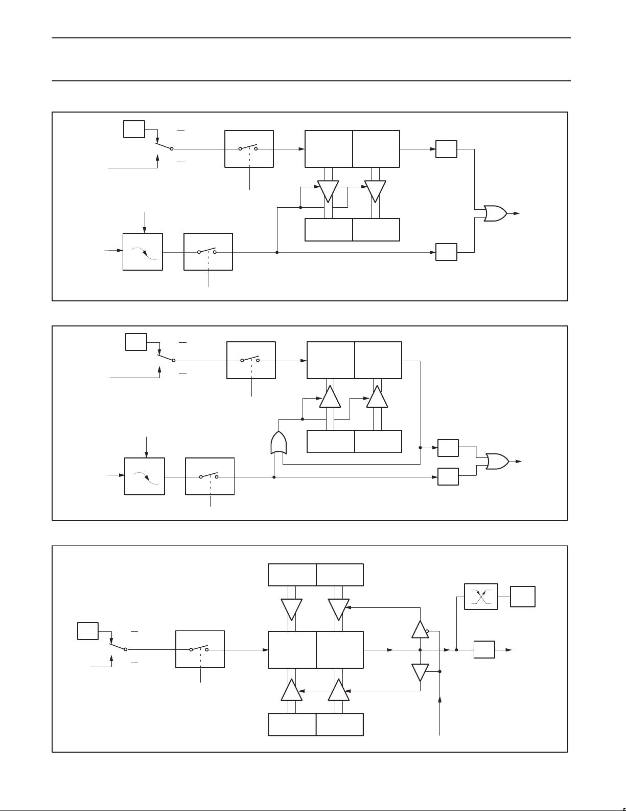
can be operated in one of three operating modes: auto-reload (up or
down counting), capture, or as the baud rate generator (for either or
both UARTs via SFRs T2MOD and T2CON). These modes are
shown in Table 1.
Capture Mode
In the capture mode there are two options which are selected by bit
EXEN2 in T2CON. If EXEN2 = 0, then timer 2 is a 16-bit timer or
counter, which upon overflowing sets bit TF2, the timer 2 overflow
bit. This will cause an interrupt when the timer 2 interrupt is enabled.
If EXEN2 = 1, then Timer 2 still does the above, but with the added
feature that a 1-to-0 transition at external input T2EX causes the
current value in the Timer 2 registers, TL2 and TH2, to be captured
into registers RCAP2L and RCAP2H, respectively. In addition, the
transition at T2EX causes bit EXF2 in T2CON to be set. This will
cause an interrupt in the same fashion as TF2 when the Timer 2
interrupt is enabled. The capture mode is illustrated in Figure 7.
Auto-Reload Mode (Up or Down Counter)
In the auto-reload mode, the timer registers are loaded with the
16-bit value in T2CAPH and T2CAPL when the count overflows.
T2CAPH and T2CAPL are initialized by software. If the EXEN2 bit in
T2CON is set, the timer registers will also be reloaded and the EXF2
flag set when a 1-to-0 transition occurs at input T2EX. The
auto-reload mode is shown in Figure 8.
In this mode, Timer 2 can be configured to count up or down. This is
done by setting or clearing the bit DCEN (Down Counter Enable) in
the T2MOD special function register (see Table 1). The T2EX pin
then controls the count direction. When T2EX is high, the count is in
the up direction, when T2EX is low, the count is in the down
direction.
Figure 8 shows Timer 2, which will count up automatically, since
DCEN = 0. In this mode there are two options selected by bit
EXEN2 in the T2CON register. If EXEN2 = 0, then Timer 2 counts
up to FFFFH and sets the TF2 (Overflow Flag) bit upon overflow.
This causes the Timer 2 registers to be reloaded with the 16-bit
value in T2CAPL and T2CAPH, whose values are preset by
software. If EXEN2 = 1, a 16-bit reload can be triggered either by an
overflow or by a 1-to-0 transition at input T2EX. This transition also
sets the EXF2 bit. If enabled, either TF2 or EXF2 bit can generate
the Timer 2 interrupt.
In Figure 9, the DCEN = 1; this enables the Timer 2 to count up or
down. In this mode, the logic level of T2EX pin controls the direction
of count. When a logic ‘1’ is applied at pin T2EX, the Timer 2 will
count up. The Timer 2 will overflow at FFFFH and set the TF2 flag,
which can then generate an interrupt if enabled. This timer overflow,
also causes the 16-bit value in T2CAPL and T2CAPH to be
reloaded into the timer registers TL2 and TH2, respectively.
A logic ‘0’ at pin T2EX causes Timer 2 to count down. When
counting down, the timer value is compared to the 16-bit value
contained in T2CAPH and T2CAPL. When the value is equal, the
1999 Apr 07
11
Page 12
Philips Semiconductors Product specification
XA 16-bit microcontroller family
32K/512 OTP/ROM/ROMless, watchdog, 2 UARTs
timer register is loaded with FFFF hex. The underflow also sets the
TF2 flag, which can generate an interrupt if enabled.
The external flag EXF2 toggles when Timer 2 underflows or
overflows. This EXF2 bit can be used as a 17th bit of resolution, if
needed. the EXF2 flag does not generate an interrupt in this mode.
As the baud rate generator, timer T2 is incremented by TCLK.
Baud Rate Generator Mode
By setting the TCLKn and/or RCLKn in T2CON or T2MOD, the
Timer 2 can be chosen as the baud rate generator for either or both
UARTs. The baud rates for transmit and receive can be
simultaneously different.
Programmable Clock-Out
A 50% duty cycle clock can be programmed to come out on P1.6.
This pin, besides being a regular I/O pin, has two alternate
functions. It can be programmed (1) to input the external clock for
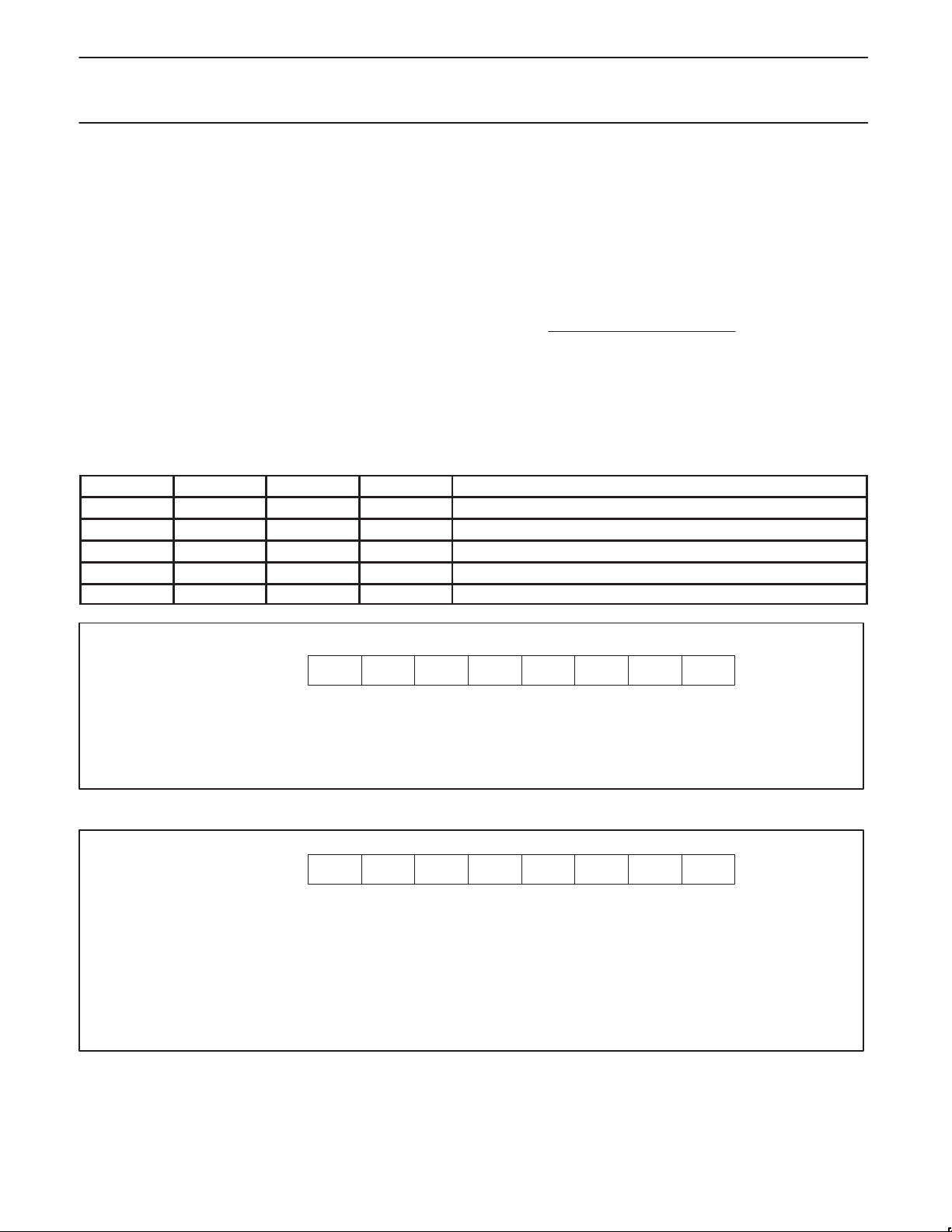
Table 1. Timer 2 Operating Modes
TR2 CP/RL2 RCLK+TCLK DCEN MODE
0 X X X Timer off (stopped)
1 0 0 0 16-bit auto-reload, counting up
1 0 0 1 16-bit auto-reload, counting up or down depending on T2EX pin
1 1 0 X 16-bit capture
1 X 1 X Baud rate generator
Timer/Counter 2 or (2) to output a 50% duty cycle clock ranging from
3.58Hz to 3.75MHz at a 30MHz operating frequency.
To configure the Timer/Counter 2 as a clock generator, bit C/T2 (in
T2CON) must be cleared and bit T20E in T2MOD must be set. Bit
TR2 (T2CON.2) also must be set to start the timer.
The Clock-Out frequency depends on the oscillator frequency and
the reload value of Timer 2 capture registers (TCAP2H, TCAP2L) as
shown in this equation:
TCLK
2 (65536 TCAP2H,TCAP2L)
In the Clock-Out mode Timer 2 roll-overs will not generate an
interrupt. This is similar to when it is used as a baud-rate generator.
It is possible to use Timer 2 as a baud-rate generator and a clock
generator simultaneously. Note, however, that the baud-rate will be
1/8 of the Clock-Out frequency.
XA-G3
TSTAT Address:411
Bit Addressable
Reset Value: 00H
BIT SYMBOL FUNCTION
TSTAT.2 T1OE When 0, this bit allows the T1 pin to clock Timer 1 when in the counter mode.
When 1, T1 acts as an output and toggles at every Timer 1 overflow.
TSTAT.0 T0OE When 0, this bit allows the T0 pin to clock Timer 0 when in the counter mode.
When 1, T0 acts as an output and toggles at every Timer 0 overflow.
Figure 5. Timer 0 And 1 Extended Status (TSTAT)
T2MOD Address:419
Bit Addressable
Reset Value: 00H
BIT SYMBOL FUNCTION
T2MOD.5 RCLK1 Receive Clock Flag.
T2MOD.4 TCLK1 Transmit Clock Flag. RCLK1 and TCLK1 are used to select Timer 2 overflow rate as a clock source
for UART1 instead of Timer T1.
T2MOD.1 T2OE When 0, this bit allows the T2 pin to clock Timer 2 when in the counter mode.
When 1, T2 acts as an output and toggles at every Timer 2 overflow .
T2MOD.0 DCEN Controls count direction for Timer 2 in autoreload mode.
DCEN=0 counter set to count up only
DCEN=1 counter set to count up or down, depending on T2EX (see text).
Figure 6. Timer 2 Mode Control (T2MOD)
—T1OE—————
T2OE——TCLK1RCLK1——
LSBMSB
T0OE
SU00612B
LSBMSB
DCEN
SU00610B
1999 Apr 07
12
Page 13
Philips Semiconductors Product specification
XA 16-bit microcontroller family
32K/512 OTP/ROM/ROMless, watchdog, 2 UARTs
T2 Pin
T2EX Pin
T2 Pin
TCLK
Transition
Detector
TCLK
C/T2
C/T2
C/T2 = 0
C/T2
= 0
= 1
= 1
EXEN2
Control
TR2
Capture
Control
Figure 7. Timer 2 in Capture Mode
Control
TL2
(8-bits)
T2CAPL T2CAPH
TL2
(8-bits)
TH2
(8-bits)
TH2
(8-bits)
TF2
EXF2
XA-G3
Timer 2
Interrupt
SU00704
T2EX Pin
T2 PIN
TCLK
Transition
Detector
C/T2 = 0
= 1
C/T2
TR2
Reload
T2CAPL T2CAPH
Control
EXEN2
Figure 8. Timer 2 in Auto-Reload Mode (DCEN = 0)
(DOWN COUNTING RELOAD VALUE)
FFH FFH
TL2 TH2
CONTROL
TR2
T2CAPL T2CAPH
OVERFLOW
TF2
EXF2
COUNT
DIRECTION
1 = UP
0 = DOWN
TOGGLE
TF2
Timer 2
Interrupt
SU00705
EXF2
INTERRUPT
1999 Apr 07
(UP COUNTING RELOAD VALUE) T2EX PIN
Figure 9. Timer 2 Auto Reload Mode (DCEN = 1)
13
SU00706
Page 14
Philips Semiconductors Product specification
XA 16-bit microcontroller family
32K/512 OTP/ROM/ROMless, watchdog, 2 UARTs
WATCHDOG TIMER
The watchdog timer subsystem protects the system from incorrect
code execution by causing a system reset when the watchdog timer
underflows as a result of a failure of software to feed the timer prior
to the timer reaching its terminal count. It is important to note that
the watchdog timer is running after any type of reset and must be
turned off by user software if the application does not use the
watchdog function.
Watchdog Function
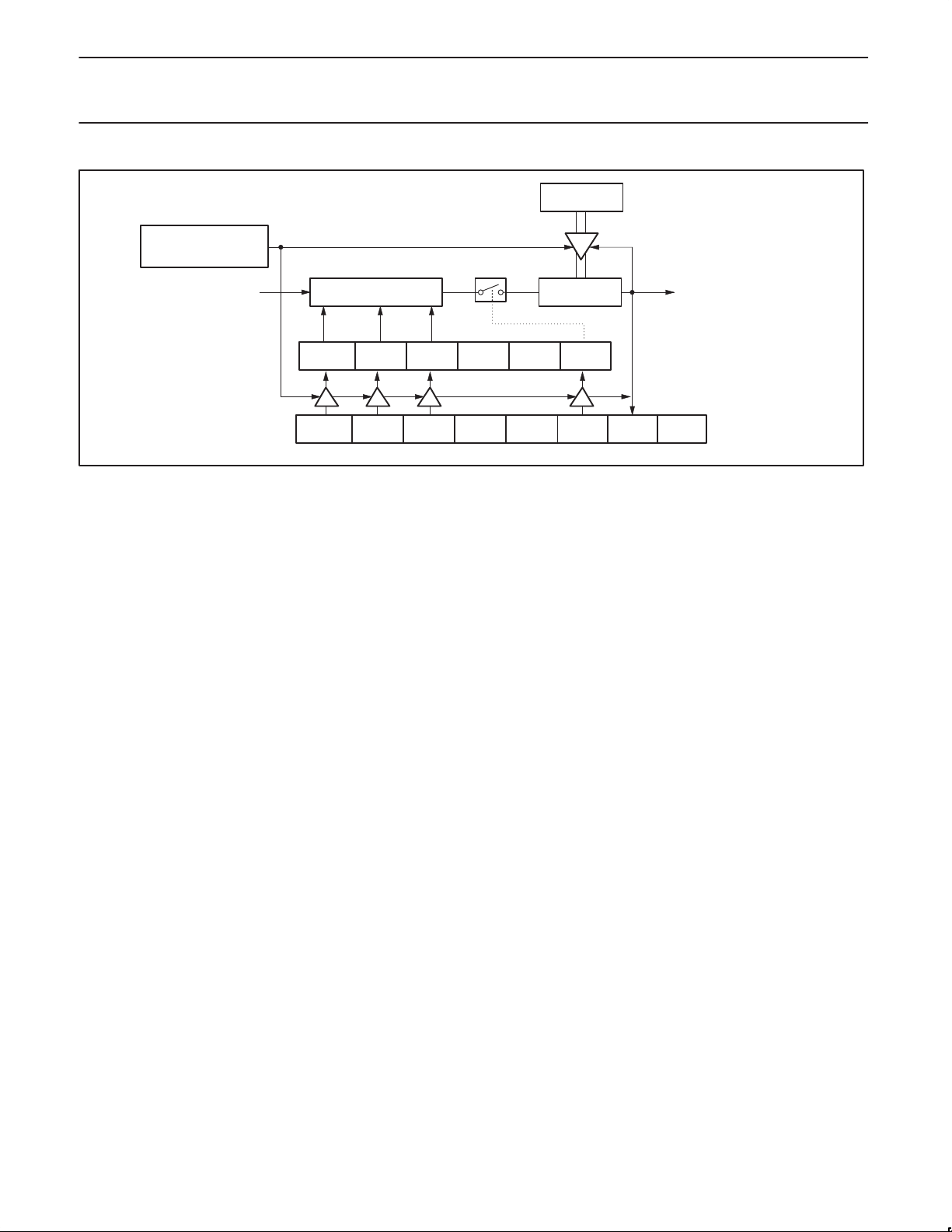
The watchdog consists of a programmable prescaler and the main
timer. The prescaler derives its clock from the TCLK source that also
drives timers 0, 1, and 2. The watchdog timer subsystem consists of
a programmable 13-bit prescaler , and an 8-bit main timer. The main
timer is clocked (decremented) by a tap taken from one of the top
8-bits of the prescaler as shown in Figure 10. The clock source for
the prescaler is the same as TCLK (same as the clock source for
the timers). Thus the main counter can be clocked as often as once
every 32 TCLKs (see Table 2). The watchdog generates an
underflow signal (and is autoloaded from WDL) when the watchdog
is at count 0 and the clock to decrement the watchdog occurs. The
watchdog is 8 bits wide and the autoload value can range from 0 to
FFH. (The autoload value of 0 is permissible since the prescaler is
cleared upon autoload).
This leads to the following user design equations. Definitions: t
is the oscillator period, N is the selected prescaler tap value, W is
the main counter autoload value, P is the prescaler value from
Table 2, t
autoload value is 0), t
autoload value is FFH), t
t
= t
MIN
t
MAX
= t
t
D
The watchdog timer is not directly loadable by the user. Instead, the
value to be loaded into the main timer is held in an autoload register.
In order to cause the main timer to be loaded with the appropriate
value, a special sequence of software action must take place. This
operation is referred to as feeding the watchdog timer.
To feed the watchdog, two instructions must be sequentially
executed successfully. No intervening SFR accesses are allowed,
so interrupts should be disabled before feeding the watchdog. The
instructions should move A5H to the WFEED1 register and then
5AH to the WFEED2 register. If WFEED1 is correctly loaded and
WFEED2 is not correctly loaded, then an immediate watchdog reset
will occur. The program sequence to feed the watchdog timer or
cause new WDCON settings to take effect is as follows:
clr ea ; disable global interrupts.
mov.b wfeed1,#A5h ; do watchdog feed part 1
mov.b wfeed2,#5Ah ; do watchdog feed part 2
setb ea ; re-enable global interrupts.
This sequence assumes that the XA interrupt system is enabled and
there is a possibility of an interrupt request occurring during the feed
sequence. If an interrupt was allowed to be serviced and the service
routine contained any SFR access, it would trigger a watchdog
reset. If it is known that no interrupt could occur during the feed
sequence, the instructions to disable and re-enable interrupts may
be removed.
is the minimum watchdog time-out value (when the
MIN
× 4 × 32 (W = 0, N = 4)
OSC
= t
× 64 × 4096 × 256 (W = 255, N = 64)
OSC
× N × P × (W + 1)
OSC
is the maximum time-out value (when the
MAX
is the design time-out value.
D
OSC
XA-G3
The software must be written so that a feed operation takes place
every t
seconds from the last feed operation. Some tradeoffs may
D
need to be made. It is not advisable to include feed operations in
minor loops or in subroutines unless the feed operation is a specific
subroutine.
To turn the watchdog timer completely off, the following code
sequence should be used:
mov.b wdcon,#0 ; set WD control register to clear WDRUN.
mov.b wfeed1,#A5h ; do watchdog feed part 1
mov.b wfeed2,#5Ah ; do watchdog feed part 2
This sequence assumes that the watchdog timer is being turned off
at the beginning of initialization code and that the XA interrupt
system has not yet been enabled. If the watchdog timer is to be
turned off at a point when interrupts may be enabled, instructions to
disable and re-enable interrupts should be added to this sequence.
Watchdog Control Register (WDCON)
The reset values of the WDCON and WDL registers will be such that
the watchdog timer has a timeout period of 4 × 4096 × t
watchdog is running. WDCON can be written by software but the
changes only take effect after executing a valid watchdog feed
sequence.
Table 2. Prescaler Select Values in WDCON
PRE2 PRE1 PRE0 DIVISOR
0 0 0 32
0 0 1 64
0 1 0 128
0 1 1 256
1 0 0 512
1 0 1 1024
1 1 0 2048
1 1 1 4096
Watchdog Detailed Operation
When external RESET is applied, the following takes place:
•Watchdog run control bit set to ON (1).
•Autoload register WDL set to 00 (min. count).
•Watchdog time-out flag cleared.
•Prescaler is cleared.
•Prescaler tap set to the highest divide.
•Autoload takes place.
When coming out of a hardware reset, the software should load the
autoload register and then feed the watchdog (cause an autoload).
If the watchdog is running and happens to underflow at the time the
external RESET is applied, the watchdog time-out flag will be
cleared.
OSC
and the
1999 Apr 07
14
Page 15
Philips Semiconductors Product specification
XA 16-bit microcontroller family
32K/512 OTP/ROM/ROMless, watchdog, 2 UARTs
WATCHDOG FEED SEQUENCE
MOV WFEED1,#A5H
MOV WFEED2,#5AH
PRESCALERTCLK
PRE2 PRE1 PRE0 — — WDRUN WDTOF
Figure 10. Watchdog Timer in XA-G3
When the watchdog underflows, the following action takes place
(see Figure 10):
•Autoload takes place.
•Watchdog time-out flag is set
•Watchdog run bit unchanged.
•Autoload (WDL) register unchanged.
•Prescaler tap unchanged.
•All other device action same as external reset.
Note that if the watchdog underflows, the program counter will be
loaded from the reset vector as in the case of an internal reset. The
watchdog time-out flag can be examined to determine if the
watchdog has caused the reset condition. The watchdog time-out
flag bit can be cleared by software.
WDCON Register Bit Definitions
WDCON.7 PRE2 Prescaler Select 2, reset to 1
WDCON.6 PRE1 Prescaler Select 1, reset to 1
WDCON.5 PRE0 Prescaler Select 0, reset to 1
WDCON.4 —
WDCON.3 —
WDCON.2 WDRUN Watchdog Run Control bit, reset to 1
WDCON.1 WDTOF Timeout flag
WDCON.0 —
UART s
The XA-G3 includes 2 UART ports that are compatible with the
enhanced UART used on the 8xC51FB. Baud rate selection is
somewhat different due to the clocking scheme used for the XA
timers.
Some other enhancements have been made to UART operation.
The first is that there are separate interrupt vectors for each UART’s
transmit and receive functions. The UART transmitter has been
double buffered, allowing packed transmission of data with no gaps
between bytes and less critical interrupt service routine timing. A
break detect function has been added to the UART. This operates
independently of the UART itself and provides a start-of-break status
bit that the program may test. Finally, an Overrun Error flag has
been added to detect missed characters in the received data
stream. The double buffered UART transmitter may require some
software changes in code written for the original XA-G3 single
buffered UART.
XA-G3
WDL
8–BIT DOWN
COUNTER
Each UART baud rate is determined by either a fixed division of the
oscillator (in UART modes 0 and 2) or by the timer 1 or timer 2
overflow rate (in UART modes 1 and 3).
Timer 1 defaults to clock both UART0 and UART1. Timer 2 can be
programmed to clock either UART0 through T2CON (via bits R0CLK
and T0CLK) or UART1 through T2MOD (via bits R1CLK and
T1CLK). In this case, the UART not clocked by T2 could use T1 as
the clock source.
The serial port receive and transmit registers are both accessed at
Special Function Register SnBUF. Writing to SnBUF loads the
transmit register, and reading SnBUF accesses a physically
separate receive register.
The serial port can operate in 4 modes:
Mode 0: Serial I/O expansion mode. Serial data enters and exits
through RxDn. TxDn outputs the shift clock. 8 bits are
transmitted/received (LSB first). (The baud rate is fixed at 1/16 the
oscillator frequency.)
Mode 1: Standard 8-bit UART mode. 10 bits are transmitted
(through TxDn) or received (through RxDn): a start bit (0), 8 data
bits (LSB first), and a stop bit (1). On receive, the stop bit goes into
RB8 in Special Function Register SnCON. The baud rate is variable.
Mode 2: Fixed rate 9-bit UART mode. 11 bits are transmitted
(through TxD) or received (through RxD): start bit (0), 8 data bits
(LSB first), a programmable 9th data bit, and a stop bit (1). On
Transmit, the 9th data bit (TB8_n in SnCON) can be assigned the
value of 0 or 1. Or, for example, the parity bit (P, in the PSW) could
be moved into TB8_n. On receive, the 9th data bit goes into RB8_n
in Special Function Register SnCON, while the stop bit is ignored.
The baud rate is programmable to 1/32 of the oscillator frequency.
Mode 3: Standard 9-bit UART mode. 11 bits are transmitted
(through TxDn) or received (through RxDn): a start bit (0), 8 data
bits (LSB first), a programmable 9th data bit, and a stop bit (1).
In fact, Mode 3 is the same as Mode 2 in all respects except baud
rate. The baud rate in Mode 3 is variable.
In all four modes, transmission is initiated by any instruction that
uses SnBUF as a destination register. Reception is initiated in
Mode 0 by the condition RI_n = 0 and REN_n = 1. Reception is
initiated in the other modes by the incoming start bit if REN_n = 1.
INTERNAL RESET
WDCON
—
SU00581A
1999 Apr 07
15
Page 16

Philips Semiconductors Product specification
XA 16-bit microcontroller family
32K/512 OTP/ROM/ROMless, watchdog, 2 UARTs
Serial Port Control Register
The serial port control and status register is the Special Function
Register SnCON, shown in Figure 12. This register contains not only
the mode selection bits, but also the 9th data bit for transmit and
receive (TB8_n and RB8_n), and the serial port interrupt bits (TI_n
and RI_n).
TI Flag
In order to allow easy use of the double buffered UART transmitter
feature, the TI_n flag is set by the UART hardware under two
conditions. The first condition is the completion of any byte
transmission. This occurs at the end of the stop bit in modes 1, 2, or
3, or at the end of the eighth data bit in mode 0. The second
condition is when SnBUF is written while the UART transmitter is
idle. In this case, the TI_n flag is set in order to indicate that the
second UART transmitter buffer is still available.
Typically, UART transmitters generate one interrupt per byte
transmitted. In the case of the XA UART, one additional interrupt is
generated as defined by the stated conditions for setting the TI_n
flag. This additional interrupt does not occur if double buffering is
bypassed as explained below. Note that if a character oriented
approach is used to transmit data through the UART, there could be
a second interrupt for each character transmitted, depending on the
timing of the writes to SBUF. For this reason, it is generally better to
bypass double buffering when the UART transmitter is used in
character oriented mode. This is also true if the UART is polled
rather than interrupt driven, and when transmission is character
oriented rather than message or string oriented. The interrupt occurs
at the end of the last byte transmitted when the UART becomes idle.
Among other things, this allows a program to determine when a
message has been transmitted completely. The interrupt service
routine should handle this additional interrupt.
XA-G3
The recommended method of using the double buffering in the
application program is to have the interrupt service routine handle a
single byte for each interrupt occurrence. In this manner the
program essentially does not require any special considerations for
double buffering. Unless higher priority interrupts cause delays in
the servicing of the UART transmitter interrupt, the double buffering
will result in transmitted bytes being tightly packed with no
intervening gaps.
9-bit Mode
Please note that the ninth data bit (TB8) is not double buffered. Care
must be taken to insure that the TB8 bit contains the intended data
at the point where it is transmitted. Double buffering of the UART
transmitter may be bypassed as a simple means of synchronizing
TB8 to the rest of the data stream.
Bypassing Double Buffering
The UART transmitter may be used as if it is single buffered. The
recommended UART transmitter interrupt service routine (ISR)
technique to bypass double buffering first clears the TI_n flag upon
entry into the ISR, as in standard practice. This clears the interrupt
that activated the ISR. Secondly, the TI_n flag is cleared
immediately following each write to SnBUF. This clears the interrupt
flag that would otherwise direct the program to write to the second
transmitter buffer. If there is any possibility that a higher priority
interrupt might become active between the write to SnBUF and the
clearing of the TI_n flag, the interrupt system may have to be
temporarily disabled during that sequence by clearing, then setting
the EA bit in the IEL register.
Note Regarding Older XA-G3 Devices
Older versions of the XA-G30, XA-G37, and XA-G35 emulation
bondout devices do not have the double buffering feature enabled.
Contact factory for details.
1999 Apr 07
16
Page 17
Philips Semiconductors Product specification
f
2
controlled by PT1, PT0
XA 16-bit microcontroller family
32K/512 OTP/ROM/ROMless, watchdog, 2 UARTs
CLOCKING SCHEME/BAUD RATE GENERATION
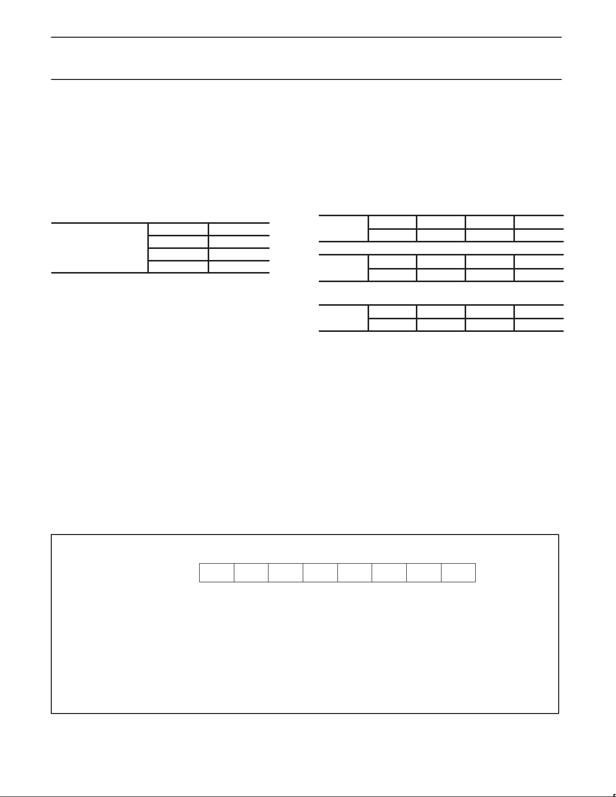
The XA UARTS clock rates are determined by either a fixed division
(modes 0 and 2) of the oscillator clock or by the Timer 1 or Timer 2
overflow rate (modes 1 and 3).
The clock for the UARTs in XA runs at 16x the Baud rate. If the
timers are used as the source for Baud Clock, since maximum
speed of timers/Baud Clock is Osc/4, the maximum baud rate is
timer overflow divided by 16 i.e. Osc/64.
In Mode 0, it is fixed at Osc/16. In Mode 2, however, the fixed rate is
Osc/32.
00 Osc/4
Pre-scaler
or all Timers T0,1,
controlled by PT1, PT0
bits in SCR
Baud Rate for UART Mode 0:
Baud_Rate = Osc/16
Baud Rate calculation for UART Mode 1 and 3:
Baud_Rate = Timer_Rate/16
Timer_Rate = Osc/(N*(Timer_Range– Timer_Reload_V alue))
where N = the TCLK prescaler value: 4, 16, or 64.
and Timer_Range = 256 for timer 1 in mode 2.
The timer reload value may be calculated as follows:
Timer_Reload_Value = Timer_Range–(Osc/(Baud_Rate*N*16))
NOTES:
1. The maximum baud rate for a UART in mode 1 or 3 is Osc/64.
2. The lowest possible baud rate (for a given oscillator frequency
and N value) may be found by using a timer reload value of 0.
3. The timer reload value may never be larger than the timer range.
4. If a timer reload value calculation gives a negative or fractional
result, the baud rate requested is not possible at the given
oscillator frequency and N value.
Baud Rate for UART Mode 2:
Baud_Rate = Osc/32
01 Osc/16
10
11 reserved
65536 for timer 1 in mode 0 and timer 2
in count up mode.
Osc/64
XA-G3
Using Timer 2 to Generate Baud Rates
Timer T2 is a 16-bit up/down counter in XA. As a baud rate
generator, timer 2 is selected as a clock source for either/both
UART0 and UART1 transmitters and/or receivers by setting TCLKn
and/or RCLKn in T2CON and T2MOD. As the baud rate generator,
T2 is incremented as Osc/N where N = 4, 16 or 64 depending on
TCLK as programmed in the SCR bits PT1, and PTO. So, if T2 is
the source of one UART, the other UART could be clocked by either
T1 overflow or fixed clock, and the UARTs could run independently
with different baud rates.
T2CON
0x418
T2MOD
0x419
Prescaler Select for Timer Clock (TCLK)
SCR
0x440
bit5 bit4
RCLK0 TCLK0
bit5 bit4
RCLK1 TCLK1
bit3 bit2
PT1 PT0
SnSTAT Address: S0STAT 421
Bit Addressable
Reset Value: 00H
1999 Apr 07
S1STAT 425
OEnBRnFEn————
BIT SYMBOL FUNCTION
SnSTAT.3 FEn Framing Error flag is set when the receiver fails to see a valid STOP bit at the end of the frame.
Cleared by software.
SnSTAT.2 BRn Break Detect flag is set if a character is received with all bits (including STOP bit) being logic ‘0’. Thus
it gives a “Start of Break Detect” on bit 8 for Mode 1 and bit 9 for Modes 2 and 3. The break detect
feature operates independently of the UARTs and provides the START of Break Detect status bit that
a user program may poll. Cleared by software.
SnSTAT.1 OEn Overrun Error flag is set if a new character is received in the receiver buffer while it is still full (before
the software has read the previous character from the buffer), i.e., when bit 8 of a new byte is
received while RI in SnCON is still set. Cleared by software.
SnSTAT.0 STINTn This flag must be set to enable any of the above status flags to generate a receive interrupt (RIn). The
only way it can be cleared is by a software write to this register.
Figure 11. Serial Port Extended Status (SnSTAT) Register
(See also Figure 13 regarding Framing Error flag)
17
LSBMSB
STINTn
SU00607B
Page 18
Philips Semiconductors Product specification
XA 16-bit microcontroller family
32K/512 OTP/ROM/ROMless, watchdog, 2 UARTs
UART INTERRUPT SCHEME
There are separate interrupt vectors for each UART’s transmit and
receive functions.
Table 3. Vector Locations for UARTs in XA
Vector Address Interrupt Source Arbitration
A0H – A3H UART 0 Receiver 7
A4H – A7H UART 0 Transmitter 8
A8H – ABH UART 1 Receiver 9
ACH – AFH UART 1 Transmitter 10
NOTE:
The transmit and receive vectors could contain the same ISR
address to work like a 8051 interrupt scheme
Error Handling, Status Flags and Break Detect
The UARTs in XA has the following error flags; see Figure 11.
Multiprocessor Communications
Modes 2 and 3 have a special provision for multiprocessor
communications. In these modes, 9 data bits are received. The 9th
one goes into RB8. Then comes a stop bit. The port can be
programmed such that when the stop bit is received, the serial port
interrupt will be activated only if RB8 = 1. This feature is enabled by
setting bit SM2 in SCON. A way to use this feature in multiprocessor
systems is as follows:
When the master processor wants to transmit a block of data to one
of several slaves, it first sends out an address byte which identifies
the target slave. An address byte differs from a data byte in that the
9th bit is 1 in an address byte and 0 in a data byte. With SM2 = 1, no
slave will be interrupted by a data byte. An address byte, however,
will interrupt all slaves, so that each slave can examine the received
byte and see if it is being addressed. The addressed slave will clear
its SM2 bit and prepare to receive the data bytes that will be coming.
The slaves that weren’t being addressed leave their SM2s set and
go on about their business, ignoring the coming data bytes.
SM2 has no effect in Mode 0, and in Mode 1 can be used to check
the validity of the stop bit although this is better done with the
Framing Error (FE) flag. In a Mode 1 reception, if SM2 = 1, the
receive interrupt will not be activated unless a valid stop bit is
received.
Automatic Address Recognition
Automatic Address Recognition is a feature which allows the UART
to recognize certain addresses in the serial bit stream by using
hardware to make the comparisons. This feature saves a great deal
of software overhead by eliminating the need for the software to
examine every serial address which passes by the serial port. This
feature is enabled by setting the SM2 bit in SCON. In the 9 bit UART
modes, mode 2 and mode 3, the Receive Interrupt flag (RI) will be
automatically set when the received byte contains either the “Given”
address or the “Broadcast” address. The 9 bit mode requires that
the 9th information bit is a 1 to indicate that the received information
is an address and not data. Automatic address recognition is shown
in Figure 14.
Using the Automatic Address Recognition feature allows a master to
selectively communicate with one or more slaves by invoking the
XA-G3
Given slave address or addresses. All of the slaves may be
contacted by using the Broadcast address. Two special Function
Registers are used to define the slave’s address, SADDR, and the
address mask, SADEN. SADEN is used to define which bits in the
SADDR are to be used and which bits are “don’t care”. The SADEN
mask can be logically ANDed with the SADDR to create the “Given”
address which the master will use for addressing each of the slaves.
Use of the Given address allows multiple slaves to be recognized
while excluding others. The following examples will help to show the
versatility of this scheme:
Slave 0 SADDR = 1100 0000
SADEN = 1111 1101
Given = 1100 00X0
Slave 1 SADDR = 1100 0000
SADEN = 1111 1110
Given = 1100 000X
In the above example SADDR is the same and the SADEN data is
used to differentiate between the two slaves. Slave 0 requires a 0 in
bit 0 and it ignores bit 1. Slave 1 requires a 0 in bit 1 and bit 0 is
ignored. A unique address for Slave 0 would be 1100 0010 since
slave 1 requires a 0 in bit 1. A unique address for slave 1 would be
1100 0001 since a 1 in bit 0 will exclude slave 0. Both slaves can be
selected at the same time by an address which has bit 0 = 0 (for
slave 0) and bit 1 = 0 (for slave 1). Thus, both could be addressed
with 1100 0000.
In a more complex system the following could be used to select
slaves 1 and 2 while excluding slave 0:
Slave 0 SADDR = 1100 0000
SADEN = 1111 1001
Given = 1100 0XX0
Slave 1 SADDR = 1110 0000
SADEN = 1111 1010
Given = 1110 0X0X
Slave 2 SADDR = 1110 0000
SADEN = 1111 1100
Given = 1110 00XX
In the above example the differentiation among the 3 slaves is in the
lower 3 address bits. Slave 0 requires that bit 0 = 0 and it can be
uniquely addressed by 1110 01 10. Slave 1 requires that bit 1 = 0 and
it can be uniquely addressed by 1110 and 0101. Slave 2 requires
that bit 2 = 0 and its unique address is 1110 0011. To select Slaves 0
and 1 and exclude Slave 2 use address 1110 0100, since it is
necessary to make bit 2 = 1 to exclude slave 2.
The Broadcast Address for each slave is created by taking the
logical OR of SADDR and SADEN. Zeros in this result are teated as
don’t-cares. In most cases, interpreting the don’t-cares as ones, the
broadcast address will be FF hexadecimal.
Upon reset SADDR and SADEN are loaded with 0s. This produces
a given address of all “don’t cares” as well as a Broadcast address
of all “don’t cares”. This effectively disables the Automatic
Addressing mode and allows the microcontroller to use standard
UART drivers which do not make use of this feature.
1999 Apr 07
18
Page 19
Philips Semiconductors Product specification
XA 16-bit microcontroller family
XA-G3
32K/512 OTP/ROM/ROMless, watchdog, 2 UARTs
SnCON Address: S0CON 420
Bit Addressable
Reset Value: 00H
BIT SYMBOL FUNCTION
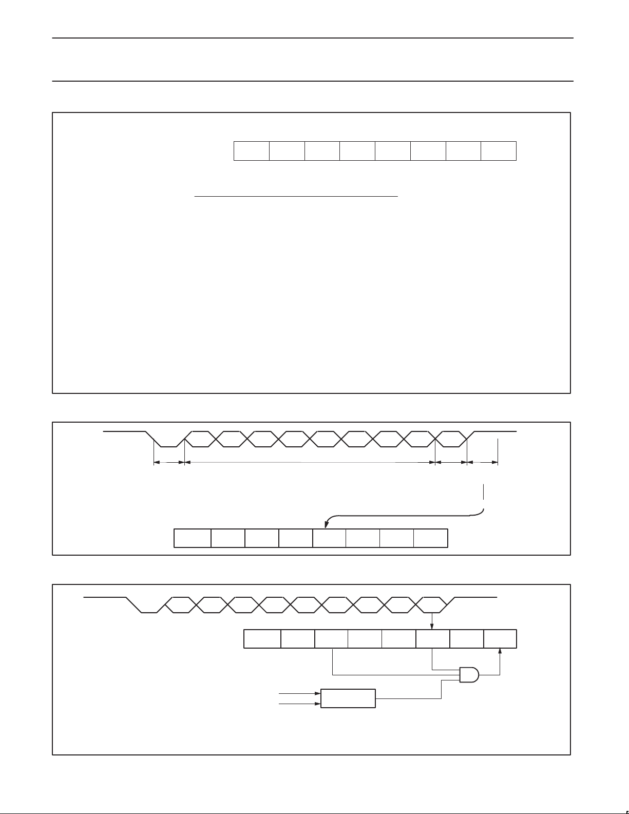
SnCON.5 SM2 Enables the multiprocessor communication feature in Modes 2 and 3. In Mode 2 or 3, if SM2 is set to 1, then Rl
SnCON.4 REN Enables serial reception. Set by software to enable reception. Clear by software to disable reception.
SnCON.3 TB8 The 9th data bit that will be transmitted in Modes 2 and 3. Set or clear by software as desired. The TB8 bit is not
SnCON.2 RB8 In Modes 2 and 3, is the 9th data bit that was received. In Mode 1, it SM2=0, RB8 is the stop bit that was
SnCON.1 TI Transmit interrupt flag. Set when another byte may be written to the UART transmitter. See text for details.
SnCON.0 RI Receive interrupt flag. Set by hardware at the end of the 8th bit time in Mode 0, or at the end of the stop bit time
S1CON 424
LSBMSB
RITIRB8TB8RENSM2SM1SM0
Where SM0, SM1 specify the serial port mode, as follows:
SM0 SM1 Mode Description Baud Rate
0 0 0 shift register f
OSC
/16
0 1 1 8-bit UART variable
1 0 2 9-bit UART f
OSC
/32
1 1 3 9-bit UART variable
will not be activated if the received 9th data bit (RB8) is 0. In Mode 1, if SM2=1 then RI will not be activated if a
valid stop bit was not received. In Mode 0, SM2 should be 0.
double buffered. See text for details.
received. In Mode 0, RB8 is not used.
Must be cleared by software.
in the other modes (except see SM2). Must be cleared by software.
SU00597C
Figure 12. Serial Port Control (SnCON) Register
D0 D1 D2 D3 D4 D5 D6 D7 D8
START
BIT
— — — — FEn BRn OEn STINTn
DATA BYTE
ONLY IN
MODE 2, 3
SnSTAT
Figure 13. UART Framing Error Detection
D0 D1 D2 D3 D4 D5 D6 D7 D8
SM0_n SM1_n SM2_n REN_n TB8_n RB8_n TI_n RI_n
1
1
RECEIVED ADDRESS D0 TO D7
PROGRAMMED ADDRESS
IN UART MODE 2 OR MODE 3 AND SM2 = 1:
INTERRUPT IF REN=1, RB8=1 AND “RECEIVED ADDRESS” = “PROGRAMMED ADDRESS”
– WHEN OWN ADDRESS RECEIVED, CLEAR SM2 TO RECEIVE DATA BYTES
– WHEN ALL DATA BYTES HAVE BEEN RECEIVED: SET SM2 TO WAIT FOR NEXT ADDRESS.
1
0
11 X
COMPARATOR
Figure 14. UART Multiprocessor Communication, Automatic Address Recognition
STOP
BIT
if 0, sets FE
SU00598
SnCON
SU00613
1999 Apr 07
19
Page 20
Philips Semiconductors Product specification
XA 16-bit microcontroller family
32K/512 OTP/ROM/ROMless, watchdog, 2 UARTs
I/O PORT OUTPUT CONFIGURA TION
Each I/O port pin can be user configured to one of 4 output types.
The types are Quasi-bidirectional (essentially the same as standard
80C51 family I/O ports), Open-Drain, Push-Pull, and Off (high
impedance). The default configuration after reset is
Quasi-bidirectional. However , in the ROMless mode (the EA
low at reset), the port pins that comprise the external data bus will
default to push-pull outputs.
I/O port output configurations are determined by the settings in port
configuration SFRs. There are 2 SFRs for each port, called
PnCFGA and PnCFGB, where “n” is the port number. One bit in
each of the 2 SFRs relates to the output setting for the
corresponding port pin, allowing any combination of the 2 output
types to be mixed on those port pins. For instance, the output type
of port 1 pin 3 is controlled by the setting of bit 3 in the SFRs
P1CFGA and P1CFGB.
Table 4 shows the configuration register settings for the 4 port
output types. The electrical characteristics of each output type may
be found in the DC Characteristic table.
Table 4. Port Configuration Register Settings
PnCFGB PnCFGA Port Output Mode
0 0 Open Drain
0 1 Quasi-bidirectional
1 0 Off (high impedance)
1 1 Push-Pull
NOTE:
Mode changes may cause glitches to occur during transitions. When
modifying both registers, WRITE instructions should be carried out
consecutively.
EXTERNAL BUS
The external program/data bus allows for 8-bit or 16-bit bus width,
and address sizes from 12 to 20 bits. The bus width is selected by
an input at reset (see Reset Options below), while the address size
is set by the program in a configuration register. If all off-chip code is
selected (through the use of the EA
be done with the maximum address size (20 bits).
pin), the initial code fetches will
RESET
The device is reset whenever a logic “0“ is applied to RST for at
least 10 microseconds, placing a low level on the pin re-initializes
the on-chip logic. Reset must be asserted when power is initially
applied to the XA and held until the oscillator is running.
The duration of reset must be extended when power is initially
applied or when using reset to exit power down mode. This is due to
the need to allow the oscillator time to start up and stabilize. For
most power supply ramp up conditions, this time is 10 milliseconds.
pin is
XA-G3
As it is brought high again, an exception is generated which causes
the processor to jump to the address contained in the memory
location 0000. The destination of the reset jump must be located in
the first 64k of code address on power-up, all vectors are 16-bit
values and so point to page zero addresses only. After a reset the
RAM contents are indeterminate.
V
DD
R
C
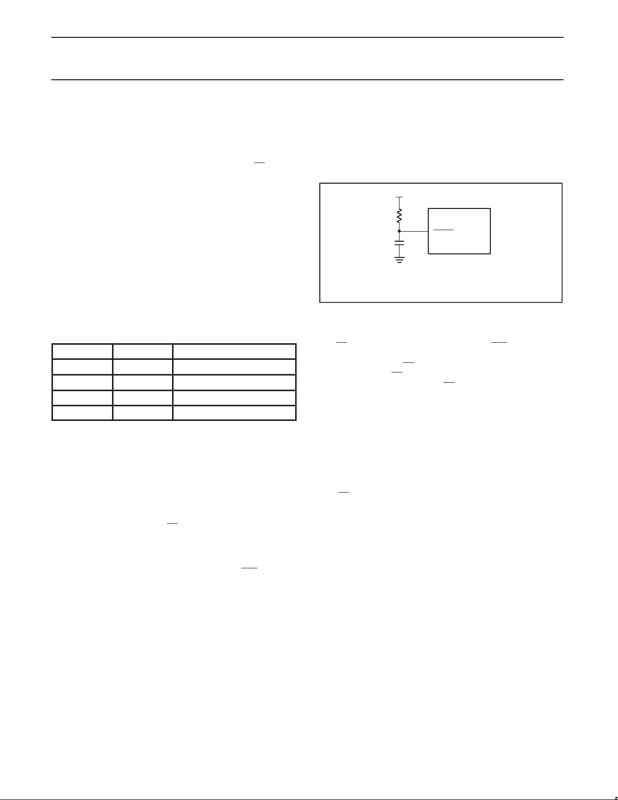
SOME TYPICAL VALUES FOR R AND C:
R = 100K, C = 1.0µF
R = 1.0M, C = 0.1µF
(ASSUMING THAT THE VDD RISE TIME IS 1ms OR LESS)
Figure 15. Recommended Reset Circuit
RESET OPTIONS
The EA pin is sampled on the rising edge of the RST pulse, and
determines whether the device is to begin execution from internal or
external code memory. EA
single-chip mode. If EA
mode. After Reset is released, the EA
signal for external bus transactions.
The BUSW/P3.5 pin is weakly pulled high while reset is asserted,
allowing simple biasing of the pin with a resistor to ground to select
the alternate bus width. If the BUSW pin is not driven at reset, the
weak pullup will cause a 1 to be loaded for the bus width, giving a
16-bit external bus. BUSW may be pulled low with a 2.7K or smaller
value resistor, giving an 8-bit external bus. The bus width setting
from the BUSW pin may be overridden by software once the user
program is running.
and BUSW must be held for three oscillator clock times
Both EA
after reset is deasserted to guarantee that their values are latched
correctly.
pulled high configures the XA in
is driven low, the device enters ROMless
POWER REDUCTION MODES
The XA-G3 supports Idle and Power Down modes of power
reduction. The idle mode leaves some peripherals running to allow
them to wake up the processor when an interrupt is generated. The
power down mode stops the oscillator in order to minimize power.
The processor can be made to exit power down mode via reset or
one of the external interrupt inputs. In order to use an external
interrupt to re-activate the XA while in power down mode, the
external interrupt must be enabled and be configured to level
sensitive mode. In power down mode, the power supply voltage may
be reduced to the RAM keep-alive voltage (2V), retaining the RAM,
register, and SFR values at the point where the power down mode
was entered.
XA
RESET
SU00702
/WAIT pin becomes a bus wait
1999 Apr 07
20
Page 21
Philips Semiconductors Product specification
XA 16-bit microcontroller family
32K/512 OTP/ROM/ROMless, watchdog, 2 UARTs
INTERRUPTS
The XA-G3 supports 38 vectored interrupt sources. These include 9
maskable event interrupts, 7 exception interrupts, 16 trap interrupts,
and 7 software interrupts. The maskable interrupts each have 8 priority
levels and may be globally and/or individually enabled or disabled.
The XA defines four types of interrupts:
•Exception Interrupts – These are system level errors and other
very important occurrences which include stack overflow,
divide-by-0, and reset.
•Event interrupts – These are peripheral interrupts from devices
such as UARTs, timers, and external interrupt inputs.
•Software Interrupts – These are equivalent of hardware
interrupt, but are requested only under software control.
•Trap Interrupts – These are TRAP instructions, generally used to
call system services in a multi-tasking system.
Exception interrupts, software interrupts, and trap interrupts are
generally standard for XA derivatives and are detailed in the
User Guide
derivatives.
. Event interrupts tend to be different on different XA
Table 5. Interrupt Vectors
XA
XA-G3
The XA-G3 supports a total of 9 maskable event interrupt sources
(for the various XA peripherals), seven software interrupts, 5
exception interrupts (plus reset), and 16 traps. The maskable event
interrupts share a global interrupt disable bit (the EA bit in the IEL
register) and each also has a separate individual interrupt enable bit
(in the IEL or IEH registers). Only three bits of the IPA register
values are used on the XA-G3. Each event interrupt can be set to
occur at one of 8 priority levels via bits in the Interrupt Priority (IP)
registers, IPA0 through IPA5. The value 0 in the IPA field gives the
interrupt priority 0, in effect disabling the interrupt. A value of 1 gives
the interrupt a priority of 9, the value 2 gives priority 10, etc. The
result is the same as if all four bits were used and the top bit set for
all values except 0. Details of the priority scheme may be found in
the XA User Guide.
The complete interrupt vector list for the XA-G3, including all 4
interrupt types, is shown in the following tables. The tables include
the address of the vector for each interrupt, the related priority
register bits (if any), and the arbitration ranking for that interrupt
source. The arbitration ranking determines the order in which
interrupts are processed if more than one interrupt of the same
priority occurs simultaneously.
EXCEPTION/TRAPS PRECEDENCE
DESCRIPTION VECTOR ADDRESS ARBITRATION RANKING
Reset (h/w, watchdog, s/w) 0000–0003 0 (High)
Breakpoint (h/w trap 1) 0004–0007 1
Trace (h/w trap 2) 0008–000B 1
Stack Overflow (h/w trap 3) 000C–000F 1
Divide by 0 (h/w trap 4) 0010–0013 1
User RETI (h/w trap 5) 0014–0017 1
TRAP 0– 15 (software) 0040–007F 1
EVENT INTERRUPTS
DESCRIPTION FLAG BIT
External interrupt 0 IE0 0080–0083 EX0 IP A0.2–0 (PX0) 2
Timer 0 interrupt TF0 0084–0087 ET0 IP A0.6–4 (PT0) 3
External interrupt 1 IE1 0088–008B EX1 IPA1.2–0 (PX1) 4
Timer 1 interrupt TF1 008C–008F ET1 IPA1.6–4 (PT1) 5
Timer 2 interrupt TF2(EXF2) 0090–0093 ET2 IP A2.2–0 (PT2) 6
Serial port 0 Rx RI.0 00A0–00A3 ERI0 IPA4.2–0 (PRIO) 7
Serial port 0 Tx TI.0 00A4–00A7 ETI0 IPA4.6–4 (PTIO) 8
Serial port 1 Rx RI.1 00A8–00AB ERI1 IPA5.2–0 (PRT1) 9
Serial port 1 Tx TI.1 00AC–00AF ETI1 IPA5.6–4 (PTI1) 10
VECTOR
ADDRESS
ENABLE BIT INTERRUPT PRIORITY
ARBITRATION
SOFTWARE INTERRUPTS
DESCRIPTION FLAG BIT
Software interrupt 1 SWR1 0100–0103 SWE1 (fixed at 1)
Software interrupt 2 SWR2 0104–0107 SWE2 (fixed at 2)
Software interrupt 3 SWR3 0108–010B SWE3 (fixed at 3)
Software interrupt 4 SWR4 010C–010F SWE4 (fixed at 4)
Software interrupt 5 SWR5 0110–0113 SWE5 (fixed at 5)
Software interrupt 6 SWR6 0114–0117 SWE6 (fixed at 6)
Software interrupt 7 SWR7 0118–011B SWE7 (fixed at 7)
VECTOR
ADDRESS
ENABLE BIT INTERRUPT PRIORITY
RANKING
1999 Apr 07
21
Page 22
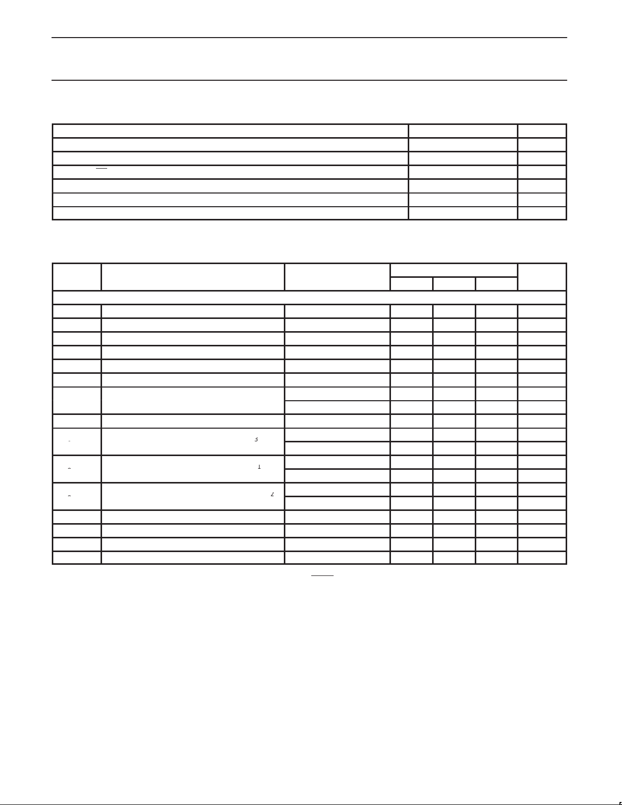
Philips Semiconductors Product specification
SYMBOL
PARAMETER
TEST CONDITIONS
UNIT
VIHInput high voltage, except XTAL1, RST
VOLOutput lo
oltage all ports, ALE, PSEN
3
V
Output high voltage all ports, ALE, PSEN
1
V
Output high voltage, ports P0–3, ALE, PSEN
2
XA 16-bit microcontroller family
XA-G3
32K/512 OTP/ROM/ROMless, watchdog, 2 UARTs
ABSOLUTE MAXIMUM RATINGS
PARAMETER RATING UNIT
Operating temperature under bias –55 to +125 °C
Storage temperature range –65 to +150 °C
Voltage on EA/VPP pin to V
Voltage on any other pin to V
SS
SS
Maximum IOL per I/O pin 15 mA
Power dissipation (based on package heat transfer limitations, not device power consumption) 1.5 W
DC ELECTRICAL CHARACTERISTICS
VDD = 2.7V to 5.5V unless otherwise specified; VDD = T
Supplies
I
I
I
I
V
V
V
C
I
I
I
DD
ID
PD
PDI
RAM
IL
IH1
OH1
OH2
IO
IL
LI
TL
Supply current operating 30 MHz 60 80 mA
Idle mode supply current 30 MHz 22 30 mA
Power-down current 5 100
Power-down current (–40°C to +85°C) 150
RAM-keep-alive voltage RAM-keep-alive voltage 1.5 V
Input low voltage –0.5 0.22V
p
p
Input high voltage to XTAL1, RST For both 3.0 & 5.0V 0.7V
p
w v
p
p
p
p
p
Input/Output pin capacitance 15 pF
Logical 0 input current, P0–3
Input leakage current, P0–3
6
5
Logical 1 to 0 transition current all ports
NOTES:
1. Ports in Quasi bi-directional mode with weak pull-up (applies to ALE, PSEN
2. Ports in Push-Pull mode, both pull-up and pull-down assumed to be same strength
3. In all output modes
4. Port pins source a transition current when used in quasi-bidirectional mode and externally driven from 1 to 0. This current is highest when
is approximately 2V .
V
IN
5. Measured with port in high impedance output mode.
6. Measured with port in quasi-bidirectional output mode.
7. Load capacitance for all outputs=80pF.
8. Under steady state (non-transient) conditions, I
Maximum I
Maximum I
Maximum total I
exceeds the test condition, VOL may exceed the related specification. Pins are not guaranteed to sink current greater than the listed
If I
OL
test conditions.
per port pin: 15mA (*NOTE: This is 85°C specification for VDD = 5V.)
OL
per 8-bit port: 26mA
OL
for all output: 71mA
OL
9. See Figures 25, 26, 29, and 30 for IDD test conditions, and Figures 27 and 28 for ICC vs. Frequency.
Max. 5V Active I
Max. 5V Idle I
Max. 3V Active I
Max. 3V Idle I
= (fosc * 1.77 mA) + 7 mA
DD
= (fosc * 0.87 mA) + 4 mA
DD
= (fosc * 0.77 mA) + 7 mA
DD
= (fosc * 0.54 mA) + 4 mA
DD
= 0 to +70°C for commercial, –40°C to +85°C for industrial, unless otherwise specified.
amb
MIN TYP MAX
At 5.0V 2.2 V
At 3.3V 2 V
DD
IOL = 3.2mA, VDD = 5.0V 0.5 V
1.0mA, VDD = 3.0V 0.4 V
IOH = –100A, VDD = 4.5V
IOH = –15A, VDD = 2.7V
2.4 V
2.0 V
IOH = 3.2mA, VDD = 4.5V 2.4 V
IOH = 1mA, VDD = 2.7V 2.2 V
VIN = 0.45V –25 –75
VIN = VIL or V
4
At 5.5V –650
IH
only during RESET).
must be externally limited as follows:
OL
0 to +13.0 V
–0.5 to VDD+0.5V V
LIMITS
A
A
DD
A
±10
A
A
V
V
1999 Apr 07
22
Page 23
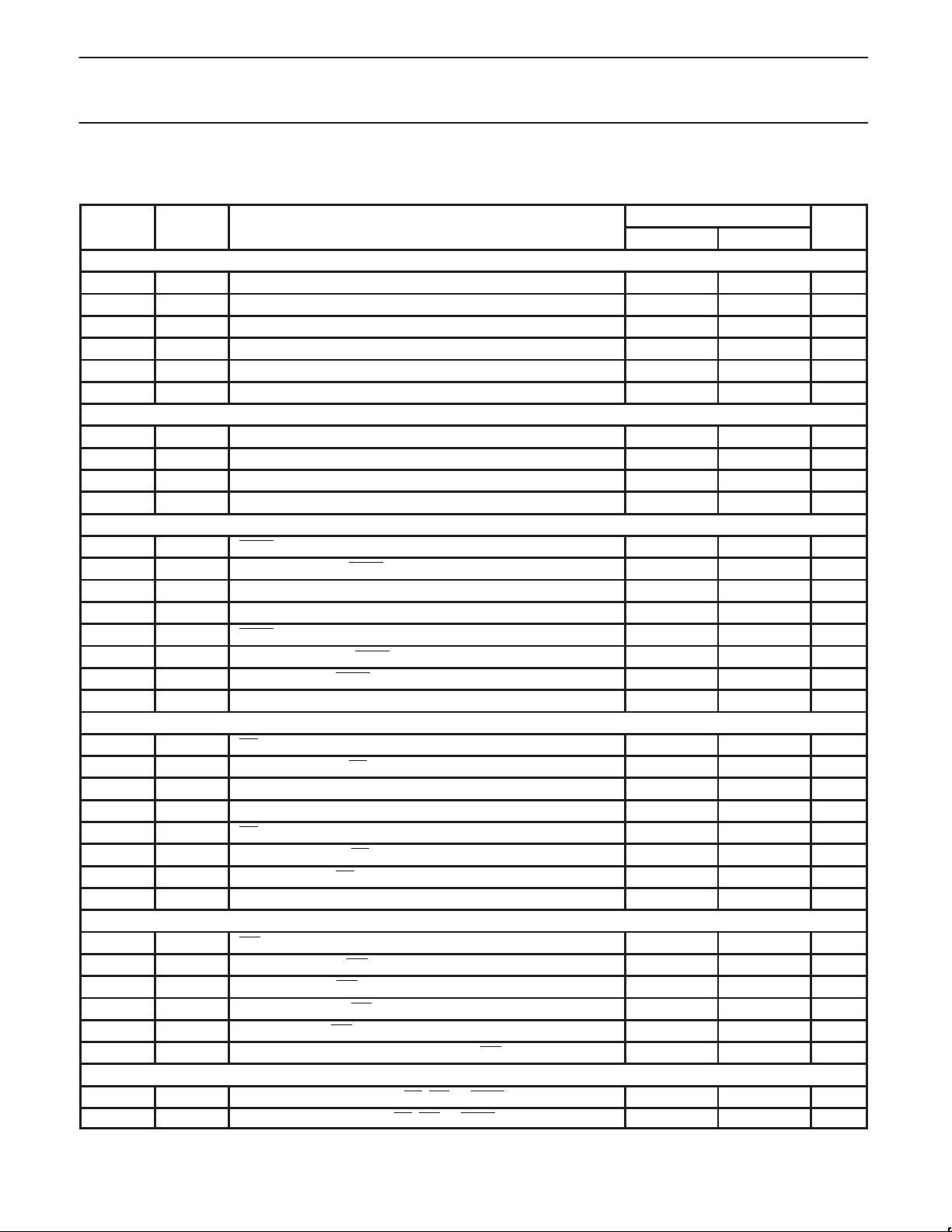
Philips Semiconductors Product specification
SYMBOL
FIGURE
PARAMETER
UNIT
XA 16-bit microcontroller family
32K/512 OTP/ROM/ROMless, watchdog, 2 UARTs
AC ELECTRICAL CHARACTERISTICS (5V)
VDD = 4.5V to 5.5V; T
External Clock
f
C
t
C
t
CHCX
t
CLCX
t
CLCH
t
CHCL
Address Cycle
t
CRAR
t
LHLL
t
AVLL
t
LLAX
Code Read Cycle
t
PLPH
t
LLPL
t
AVIVA
t
AVIVB
t
PLIV
t
PXIX
t
PXIZ
t
IXUA
Data Read Cycle
t
RLRH
t
LLRL
t
AVDVA
t
AVDVB
t
RLDV
t
RHDX
t
RHDZ
t
DXUA
Data Write Cycle
t
WLWH
t
LLWL
t
QVWX
t
WHQX
t
AVWL
t
UAWH
Wait Input
t
WTH
t
WTL
NOTES ON PAGE 24.
= 0 to +70°C for commercial, –40°C to +85°C for industrial.
amb
Oscillator frequency 0 30 MHz
22 Clock period and CPU timing cycle 1/f
22 Clock high time tC * 0.5 ns
22 Clock low time tC * 0.4 ns
22 Clock rise time 5 ns
22 Clock fall time 5 ns
21 Delay from clock rising edge to ALE rising edge 10 46 ns
16 ALE pulse width (programmable) (V1 * tC) – 6 ns
16 Address valid to ALE de-asserted (set-up) (V1 * tC) – 12 ns
16 Address hold after ALE de-asserted (tC/2) – 10 ns
16 PSEN pulse width (V2 * tC) – 10 ns
16 ALE de-asserted to PSEN asserted (tC/2) – 7 ns
16 Address valid to instruction valid, ALE cycle (access time) (V3 * tC) – 36 ns
17 Address valid to instruction valid, non-ALE cycle (access time) (V4 * tC) – 29 ns
16 PSEN asserted to instruction valid (enable time) (V2 * tC) – 29 ns
16 Instruction hold after PSEN de-asserted 0 ns
16 Bus 3-State after PSEN de-asserted (disable time) tC – 8 ns
16 Hold time of unlatched part of address after instruction latched 0 ns
18 RD pulse width (V7 * tC) – 10 ns
18 ALE de-asserted to RD asserted (tC/2) – 7 ns
18 Address valid to data input valid, ALE cycle (access time) (V6 * tC) – 36 ns
19 Address valid to data input valid, non-ALE cycle (access time) (V5 * tC) – 29 ns
18 RD low to valid data in, enable time (V7 * tC) – 29 ns
18 Data hold time after RD de-asserted 0 ns
18 Bus 3-State after RD de-asserted (disable time) tC – 8 ns
18 Hold time of unlatched part of address after data latched 0 ns
20 WR pulse width (V8 * tC) – 10 ns
20 ALE falling edge to WR asserted (V12 * tC) – 10 ns
20 Data valid before WR asserted (data setup time) (V13 * tC) – 22 ns
20 Data hold time after WR de-asserted (Note 6) (V11 * tC) – 5 ns
20 Address valid to WR asserted (address setup time) (Note 5) (V9 * tC) – 22 ns
20 Hold time of unlatched part of address after WR is de-asserted (V11 * tC) – 7 ns
21 WAIT stable after bus strobe (RD, WR, or PSEN) asserted (V10 * tC) – 30 ns
21 WAIT hold after bus strobe (RD, WR, or PSEN) assertion (V10 * tC) – 5 ns
VARIABLE CLOCK
MIN MAX
C
XA-G3
ns
1999 Apr 07
23
Page 24
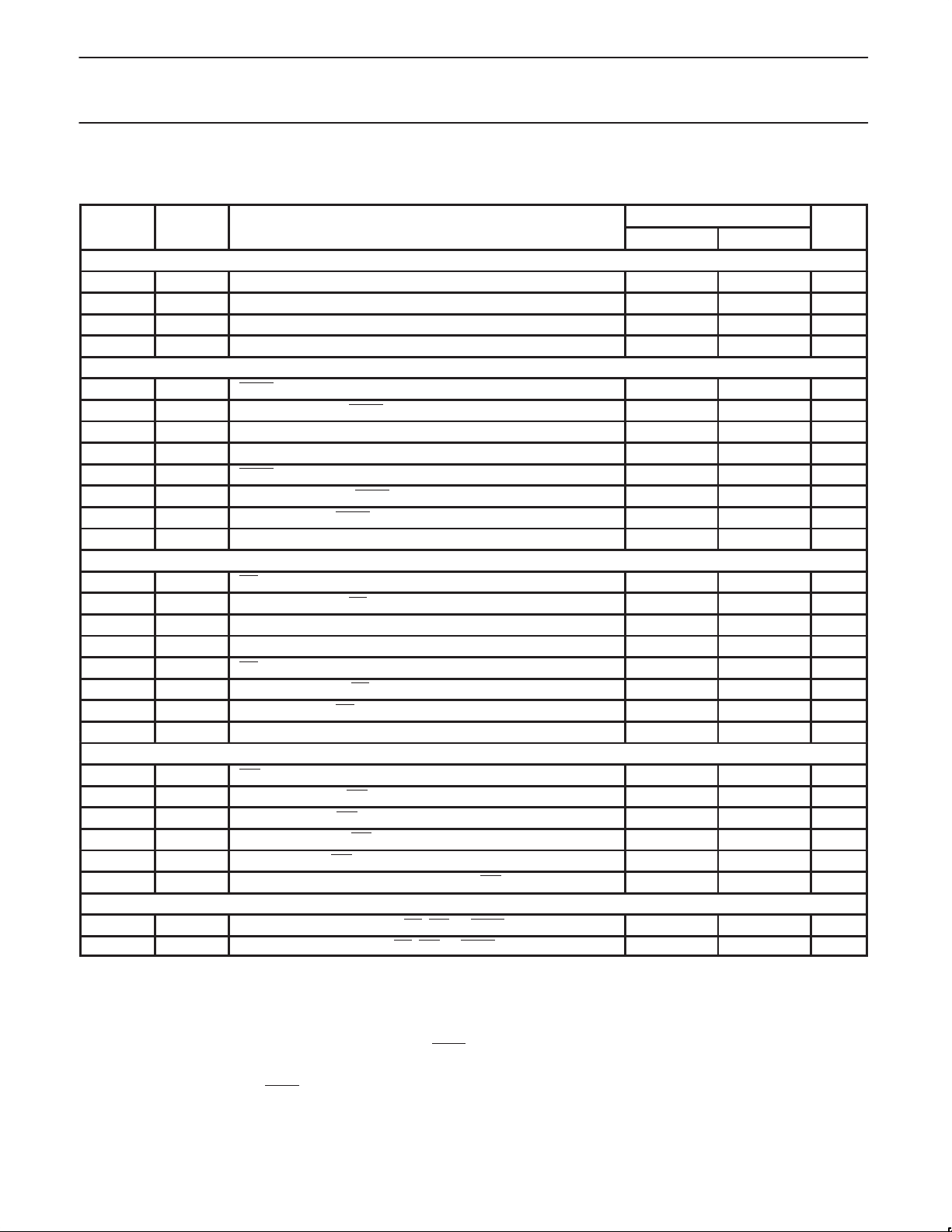
Philips Semiconductors Product specification
SYMBOL
FIGURE
PARAMETER
UNIT
XA 16-bit microcontroller family
XA-G3
32K/512 OTP/ROM/ROMless, watchdog, 2 UARTs
AC ELECTRICAL CHARACTERISTICS (3V)
VDD = 2.7V to 5.5V; T
Address Cycle
t
CRAR
t
LHLL
t
AVLL
t
LLAX
Code Read Cycle
t
PLPH
t
LLPL
t
AVIVA
t
AVIVB
t
PLIV
t
PXIX
t
PXIZ
t
IXUA
Data Read Cycle
t
RLRH
t
LLRL
t
AVDVA
t
AVDVB
t
RLDV
t
RHDX
t
RHDZ
t
DXUA
Data Write Cycle
t
WLWH
t
LLWL
t
QVWX
t
WHQX
t
AVWL
t
UAWH
Wait Input
t
WTH
t
WTL
NOTES:
1. Load capacitance for all outputs = 80pF.
2. Variables V1 through V13 reflect programmable bus timing, which is programmed via the Bus Timing registers (BTRH and BTRL).
Refer to the
XA User Guide
V1) This variable represents the programmed width of the ALE pulse as determined by the ALEW bit in the BTRL register.
V1 = 0.5 if the ALEW bit = 0, and 1.5 if the ALEW bit = 1.
V2) This variable represents the programmed width of the PSEN
ALEW bits in the BTRL register.
– For a bus cycle with no ALE, V2 = 1 if CR1/0 = 00, 2 if CR1/0 = 01, 3 if CR1/0 = 10, and 4 if CR1/0 = 11. Note that during burst
mode code fetches, PSEN
determining peripheral timing requirements.
– For a bus cycle with an ALE, V2 = the total bus cycle duration (2 if CRA1/0 = 00, 3 if CRA1/0 = 01, 4 if CRA1/0 = 10,
and 5 if CRA1/0 = 11) minus the number of clocks used by ALE (V1 + 0.5).
Example: If CRA1/0 = 10 and ALEW = 1, the V2 = 4 – (1.5 + 0.5) = 2.
= 0 to +70°C for commercial, –40°C to +85°C for industrial.
amb
VARIABLE CLOCK
MIN MAX
21 Delay from clock rising edge to ALE rising edge 15 60 ns
16 ALE pulse width (programmable) (V1 * tC) – 10 ns
16 Address valid to ALE de-asserted (set-up) (V1 * tC) – 18 ns
16 Address hold after ALE de-asserted (tC/2) – 12 ns
16 PSEN pulse width (V2 * tC) – 12 ns
16 ALE de-asserted to PSEN asserted (tC/2) – 9 ns
16 Address valid to instruction valid, ALE cycle (access time) (V3 * tC) – 58 ns
17 Address valid to instruction valid, non-ALE cycle (access time) (V4 * tC) – 52 ns
16 PSEN asserted to instruction valid (enable time) (V2 * tC) – 52 ns
16 Instruction hold after PSEN de-asserted 0 ns
16 Bus 3-State after PSEN de-asserted (disable time) tC – 8 ns
16 Hold time of unlatched part of address after instruction latched 0 ns
18 RD pulse width (V7 * tC) – 12 ns
18 ALE de-asserted to RD asserted (tC/2) – 9 ns
18 Address valid to data input valid, ALE cycle (access time) (V6 * tC) – 58 ns
19 Address valid to data input valid, non-ALE cycle (access time) (V5 * tC) – 52 ns
18 RD low to valid data in, enable time (V7 * tC) – 52 ns
18 Data hold time after RD de-asserted 0 ns
18 Bus 3-State after RD de-asserted (disable time) tC – 8 ns
18 Hold time of unlatched part of address after data latched 0 ns
20 WR pulse width (V8 * tC) – 12 ns
20 ALE falling edge to WR asserted (V12 * tC) – 10 ns
20 Data valid before WR asserted (data setup time) (V13 * tC) – 28 ns
20 Data hold time after WR de-asserted (Note 6) (V11 * tC) – 8 ns
20 Address valid to WR asserted (address setup time) (Note 5) (V9 * tC) – 28 ns
20 Hold time of unlatched part of address after WR is de-asserted (V11 * tC) – 10 ns
21 WAIT stable after bus strobe (RD, WR, or PSEN) asserted (V10 * tC) – 40 ns
21 WAIT hold after bus strobe (RD, WR, or PSEN) assertion (V10 * tC) – 5 ns
for details of the bus timing settings.
pulse as determined by the CR1 and CR0 bits or the CRA1, CRA0, and
does not exhibit transitions at the boundaries of bus cycles. V2 still applies for the purpose of
1999 Apr 07
24
Page 25

Philips Semiconductors Product specification
XA 16-bit microcontroller family
XA-G3
32K/512 OTP/ROM/ROMless, watchdog, 2 UARTs
V3) This variable represents the programmed length of an entire code read cycle with ALE. This time is determined by the CRA1 and
CRA0 bits in the BTRL register. V3 = the total bus cycle duration (2 if CRA1/0 = 00, 3 if CRA1/0 = 01, 4 if CRA1/0 = 10,
and 5 if CRA1/0 = 11).
V4) This variable represents the programmed length of an entire code read cycle with no ALE. This time is determined by the CR1 and
CR0 bits in the BTRL register. V4 = 1 if CR1/0 = 00, 2 if CR1/0 = 01, 3 if CR1/0 = 10, and 4 if CR1/0 = 11.
V5) This variable represents the programmed length of an entire data read cycle with no ALE. this time is determined by the DR1 and
DR0 bits in the BTRH register. V5 = 1 if DR1/0 = 00, 2 if DR1/0 = 01, 3 if DR1/0 = 10, and 4 if DR1/0 = 11.
V6) This variable represents the programmed length of an entire data read cycle with ALE. The time is determined by the DRA1 and
DRA0 bits in the BTRH register. V6 = the total bus cycle duration (2 if DRA1/0 = 00, 3 if DRA1/0 = 01, 4 if DRA1/0 = 10,
and 5 if DRA1/0 = 11).
V7) This variable represents the programmed width of the RD
BTRH register, and the ALEW bit in the BTRL register. Note that during a 16-bit operation on an 8-bit external bus, RD
and does not exhibit a transition between the first and second byte bus cycles. V7 still applies for the purpose of determining
peripheral timing requirements. The timing for the first byte is for a bus cycle with ALE, the timing for the second byte is for a bus
cycle with no ALE.
– For a bus cycle with no ALE, V7 = 1 if DR1/0 = 00, 2 if DR1/0 = 01, 3 if DR1/0 = 10, and 4 if DR1/0 = 11.
– For a bus cycle with an ALE, V7 = the total bus cycle duration (2 if DRA1/0 = 00, 3 if DRA1/0 = 01, 4 if DRA1/0 = 10,
and 5 if DRA1/0 = 11) minus the number of clocks used by ALE (V1 + 0.5).
V8) This variable represents the programmed width of the WRL and/or WRH pulse as determined by the WM1 bit in the BTRL register.
V9) This variable represents the programmed address setup time for a write as determined by the data write cycle duration (defined by
V10) This variable represents the length of a bus strobe for calculation of WAIT setup and hold times. The strobe may be RD
V11) This variable represents the programmed write hold time as determined by the WM0 bit in the BTRL register.
V12) This variable represents the programmed period between the end of the ALE pulse and the beginning of the WRL
V13) This variable represents the programmed data setup time for a write as determined by the data write cycle duration (defined by DW1
3. Not all combinations of bus timing configuration values result in valid bus cycles. Please refer to the XA User Guide section on the External
Bus for details.
4. When code is being fetched for execution on the external bus, a burst mode fetch is used that does not have PSEN
cycle. Thus, if WAIT is used to delay code fetch cycles, a change in the low order address lines must be detected to locate the beginning of
a cycle. This would be A3–A0 for an 8-bit bus, and A3–A1 for a 16-bit bus. Also, a 16-bit data read operation conducted on a 8-bit wide bus
similarly does not include two separate RD
the second half of such a cycle.
5. This parameter is provided for peripherals that have the data clocked in on the falling edge of the WR
and in most applications this parameter is not used.
6. Please note that the XA-G3 requires that extended data bus hold time (WM0 = 1) to be used with external bus write cycles.
Example: If DRA1/0 = 00 and ALEW = 0, then V7 = 2 – (0.5 + 0.5) = 1.
V8 1 if WM1 = 0, and 2 if WM1 = 1.
DW1 and DW0 or the DWA1 and DWA0 bits in the BTRH register), the WM0 bit in the BTRL register, and the value of V8.
– For a bus cycle with an ALE, V9 = the total bus write cycle duration (2 if DWA1/0 = 00, 3 if DWA1/0 = 01, 4 if DWA1/0 = 10, and
5 if DWA1/0 = 11) minus the number of clocks used by the WRL
hold time (0 if WM0 = 0 and 1 if WM0 = 1).
Example: If DWA1/0 = 10, WM0 = 1, and WM1 = 1, then V9 = 4 – 1 – 2 = 1.
– For a bus cycle with no ALE, V9 = the total bus cycle duration (2 if DW1/0 = 00, 3 if DW1/0 = 01, 4 if DW1/0 = 10, and
5 if DW1/0 = 11) minus the number of clocks used by the WRL
hold time (0 if WM0 = 0 and 1 if WM0 = 1).
Example: If DW1/0 = 11, WM0 = 1, and WM1 = 0, then V9 = 5 – 1 – 1 = 3.
cycles), WRL
by WAIT. V10 = V2 for WAIT associated with a code read cycle using PSEN
V10 = V7–1 for a data read cycle using RD
If WAIT is used to vary the duration of data read cycles, the RD
Also see Note 4.
V11 = 0 if the WM0 bit = 0, and 1 if the WM0 bit = 1.
as determined by the data write cycle duration (defined by the DWA1 and DWA0 bits in the BTRH register), the WM0 bit in the BTR L
register, and the values of V1 and V8. V12 = the total bus cycle duration (2 if DWA1/0 = 00, 3 if DWA1/0 = 01, 4 if DWA1/0 = 10, and 5
if DWA1/0 = 11) minus the number of clocks used by the WRL
time (0 if WM0 = 0 and 1 if WM0 = 1), minus the width of the ALE pulse (V1).
Example: If DWA1/0 = 11, WM0 = 1, WM1 = 0, and ALEW = 1, then V12 = 5 – 1 – 1 – 1.5 = 1.5.
and DW0 or the DWA1 and DWA0 bits in the BTRH register), the WM0 bit in the BTRL register, and the values of V1 and V8.
– For a bus cycle with an ALE, V13 = the total bus cycle duration (2 if DWA1/0 = 00, 3 if DWA1/0 = 01, 4 if DWA1/0 = 10, and
5 if DWA1/0 = 11) minus the number of clocks used by the WRL
data hold time (0 if WM0 = 0 and 1 if WM0 = 1), minus the number of clocks used by ALE (V1 + 0.5).
Example: If DWA1/0 = 11, WM0 = 1, WM1 = 1, and ALEW = 0, then V13 = 5 – 1 – 2 – 1 = 1.
– For a bus cycle with no ALE, V13 = the total bus cycle duration (2 if DW1/0 = 00, 3 if DW1/0 = 01, 4 if DW1/0 = 10, and
5 if DW1/0 = 11) minus the number of clocks used by the WRL
data hold time (0 if WM0 = 0 and 1 if WM0 = 1).
Example: If DW1/0 = 01, WM0 = 1, and WM1 = 0, then V13 = 3 – 1 – 1 = 1.
and/or WRH (for data write cycles), or PSEN (for code read cycles), depending on the type of bus cycle being widened
. This means that a single clock data read cycle cannot be stretched using WAIT.
strobes. So, a rising edge on the low order address line (A0) must be used to trigger a WAIT in
pulse as determined by the DR1 and DR0 bits or the DRA1, DRA0 in the
remains low
and/or WRH pulse (V8), minus the number of clocks used by data
and/or WRH pulse (V8), minus the number of clocks used by data
(for data read
. V10 = V8 for a data write cycle using WRL and/or WRH.
strobe width must be set to be at least two clocks in duration.
and/or WRH pulse
and/or WRH pulse (V8), minus the number of clocks used by data hold
and/or WRH pulse (V8), minus the number of clocks used by
and/or WRH pulse (V8), minus the number of clocks used by
edges in every fetch
strobe. This is not usually the case,
1999 Apr 07
25
Page 26
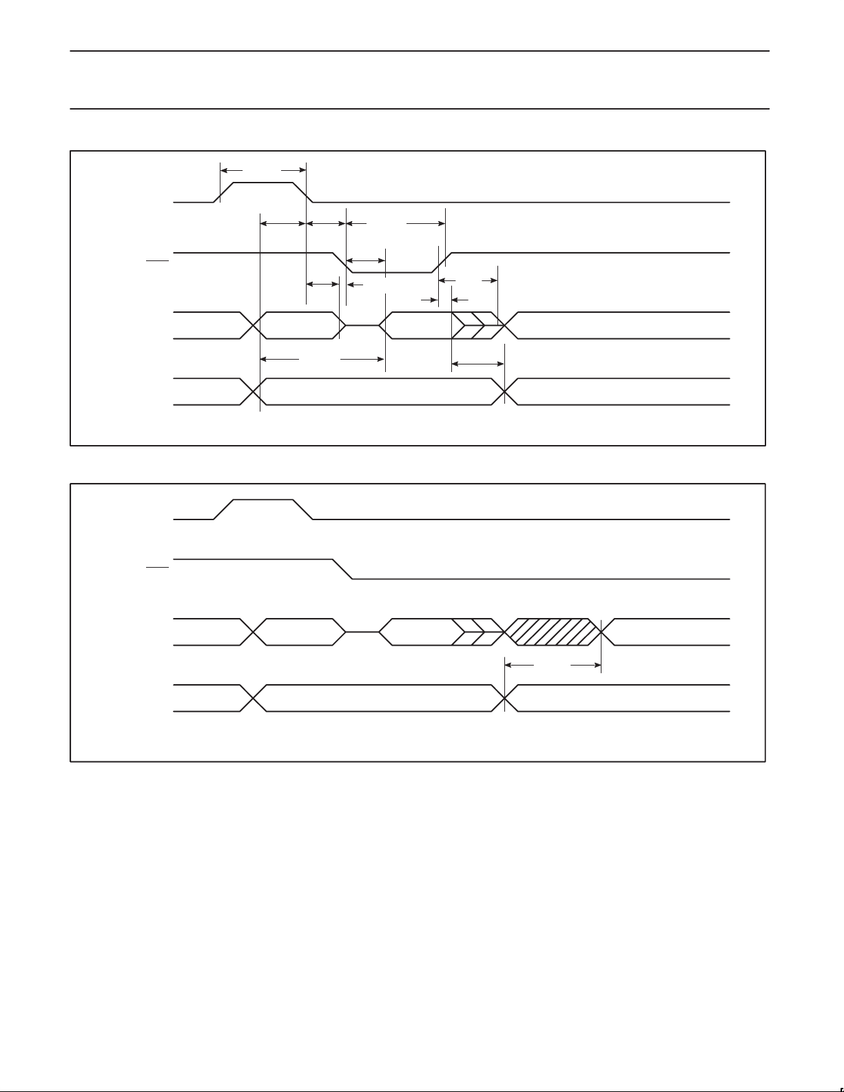
Philips Semiconductors Product specification
XA 16-bit microcontroller family
32K/512 OTP/ROM/ROMless, watchdog, 2 UARTs
t
LHLL
ALE
t
PSEN
MULTIPLEXED
ADDRESS AND DATA
UNMULTIPLEXED
ADDRESS
A4–A11 or A4–A19
* INSTR IN is either D0–D7 or D0–D15, depending on the bus width (8 or 16 bits).
Figure 16. External Program Memory Read Cycle (ALE Cycle)
AVLL
t
LLPL
t
LLAX
t
AVIVA
A0 or A1–A3, A12–19
t
PLIV
t
PLPH
t
PLAZ
t
PXIX
INSTR IN *
t
PXIZ
t
IXUA
XA-G3
SU00946
ALE
PSEN
MULTIPLEXED
ADDRESS AND DATA
UNMULTIPLEXED
ADDRESS
A4–A11 or A4–A19
A0 or A1–A3, A12–19
INSTR IN
*
* INSTR IN is either D0–D7 or D0–D15, depending on the bus width (8 or 16 bits).
Figure 17. External Program Memory Read Cycle (Non-ALE Cycle)
t
AVIVB
A0 or A1–A3, A12–19
SU00707
1999 Apr 07
26
Page 27
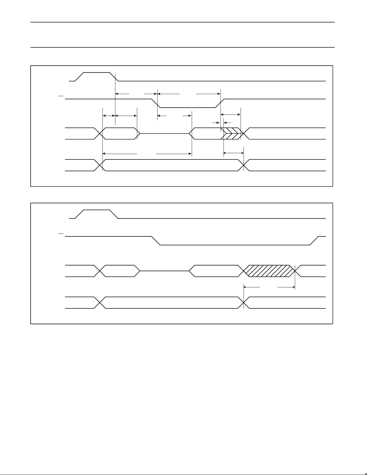
Philips Semiconductors Product specification
XA 16-bit microcontroller family
32K/512 OTP/ROM/ROMless, watchdog, 2 UARTs
ALE
t
t
LLAX
LLRL
t
AVDVA
A0 or A1–A3, A12–A19
RD
MULTIPLEXED
ADDRESS
AND DATA
UNMULTIPLEXED
ADDRESS
t
AVLL
A4–A11 or A4–A19
* DATA IN is either D0–D7 or D0–D15, depending on the bus width (8 or 16 bits).
Figure 18. External Data Memory Read Cycle (ALE Cycle)
t
RLDV
t
RLRH
t
RHDX
DATA IN *
t
RHDZ
t
DXUA
XA-G3
SU00947
ALE
MULTIPLEXED
ADDRESS
AND DATA
UNMULTIPLEXED
ADDRESS
RD
A4–A11
A0–A3, A12–A19
D0–D7
t
AVDVB
Figure 19. External Data Memory Read Cycle (Non-ALE Cycle) 8 Bit Bus Only
A0–A3, A12–A19
DATA IN
SU00708A
*
1999 Apr 07
27
Page 28
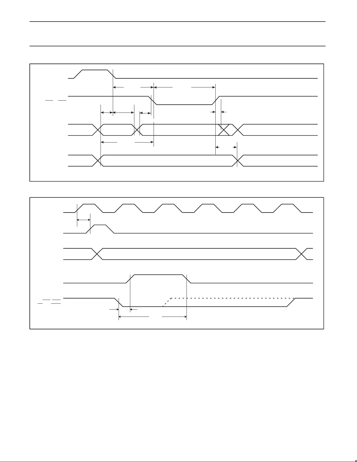
Philips Semiconductors Product specification
XA 16-bit microcontroller family
32K/512 OTP/ROM/ROMless, watchdog, 2 UARTs
ALE
t
LLWL
or WRH
WRL
MULTIPLEXED
ADDRESS
AND DATA
UNMULTIPLEXED
ADDRESS
t
AVLL
t
LLAX
A4–A11 or A4–A15
t
AVWL
t
QVWX
A0 or A1–A3, A12–A19
* DATA OUT is either D0–D7 or D0–D15, depending on the bus width (8 or 16 bits).
Figure 20. External Data Memory Write Cycle
t
WLWH
DATA OUT
*
t
UAWH
t
WHQX
XA-G3
SU00584C
XTAL1
ALE
ADDRESS BUS
WAIT
BUS STROBE
(WRL, WRH,
RD, OR PSEN)
t
CRAR
t
WTH
t
WTL
Figure 21. WAIT Signal Timing
(The dashed line shows the strobe without WAIT.)
SU00709A
1999 Apr 07
28
Page 29
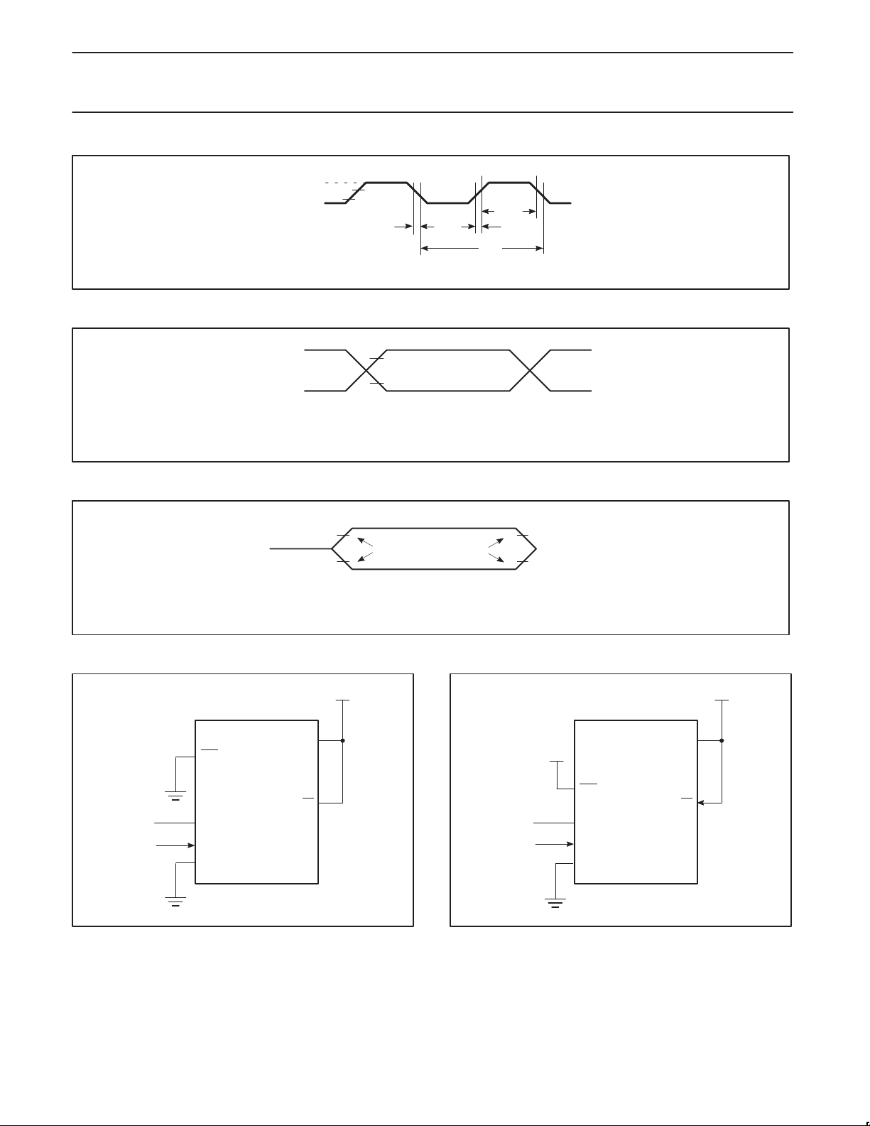
Philips Semiconductors Product specification
XA 16-bit microcontroller family
32K/512 OTP/ROM/ROMless, watchdog, 2 UARTs
VDD–0.5
0.45V
VDD–0.5
0.45V
NOTE:
AC inputs during testing are driven at VDD –0.5 for a logic ‘1’ and 0.45V for a logic ‘0’.
Timing measurements are made at the 50% point of transitions.
0.7V
DD
0.2VDD–0.1
t
CHCL
t
CLCX
Figure 22. External Clock Drive
0.2V
+0.9
DD
0.2V
–0.1
DD
Figure 23. AC Testing Input/Output
t
C
t
CHCX
t
CLCH
XA-G3
SU00842
SU00703A
V
LOAD
NOTE:
For timing purposes, a port is no longer floating when a 100mV change from load voltage occurs,
and begins to float when a 100mV change from the loaded V
RST
(NC)
CLOCK SIGNAL
XTAL2
XTAL1
V
SS
Figure 25. IDD Test Condition, Active Mode
All other pins are disconnected
V
LOAD
V
LOAD
+0.1V
–0.1V
V
DD
EA
SU00591B
TIMING
REFERENCE
POINTS
Figure 24. Float Waveform
V
DD
V
OH
V
OL
level occurs. IOH/IOL ≥ ±20mA.
OH/VOL
(NC)
CLOCK SIGNAL
Figure 26. IDD Test Condition, Idle Mode
All other pins are disconnected
V
–0.1V
+0.1V
DD
SU00011
RST
XTAL2
XTAL1
V
SS
V
DD
EA
SU00590B
V
DD
1999 Apr 07
29
Page 30
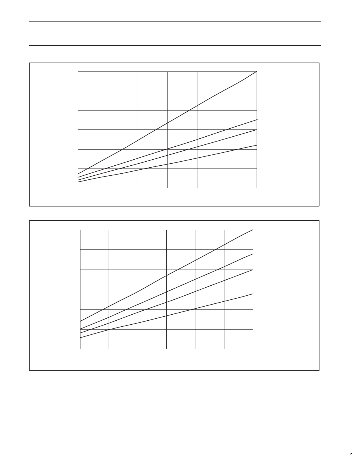
Philips Semiconductors Product specification
XA 16-bit microcontroller family
32K/512 OTP/ROM/ROMless, watchdog, 2 UARTs
60
50
40
mA
30
20
10
0
0 5 10 15 20 25 30
FREQUENCY
Figure 27. IDD vs. Frequency at VDD = 5.0V
MAX. I
DD
TYPICAL I
MAX. I
DD
TYPICAL I
(ACTIVE)
(ACTIVE)
DD
(IDLE)
(IDLE)
DD
SU01192
XA-G3
30
25
20
15
mA
10
5
0
0 5 10 15 20 25 30
FREQUENCY
Figure 28. IDD vs. Frequency at VDD = 3.0V
(ACTIVE)
MAX. I
DD
TYPICAL I
MAX. IDD (IDLE)
TYPICAL I
(ACTIVE)
DD
(IDLE)
DD
SU01193
1999 Apr 07
30
Page 31
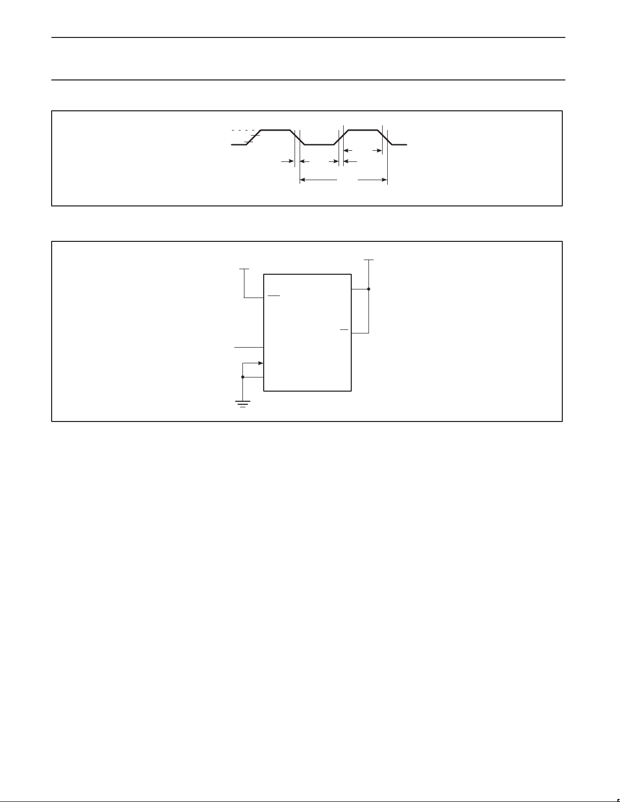
Philips Semiconductors Product specification
XA 16-bit microcontroller family
32K/512 OTP/ROM/ROMless, watchdog, 2 UARTs
VDD–0.5
0.45V
Figure 29. Clock Signal Waveform for IDD Tests in Active and Idle Modes
(NC)
V
DD
0.7V
DD
0.2VDD–0.1
t
CHCL
t
CLCH
RST
XTAL2
XTAL1
V
SS
= t
t
CLCX
CHCL
= 5ns
XA-G3
t
CHCX
t
CLCH
t
CL
SU00608A
V
DD
V
DD
EA
SU00585A
Figure 30. IDD Test Condition, Power Down Mode
All other pins are disconnected. V
=2V to 5.5V
DD
1999 Apr 07
31
Page 32
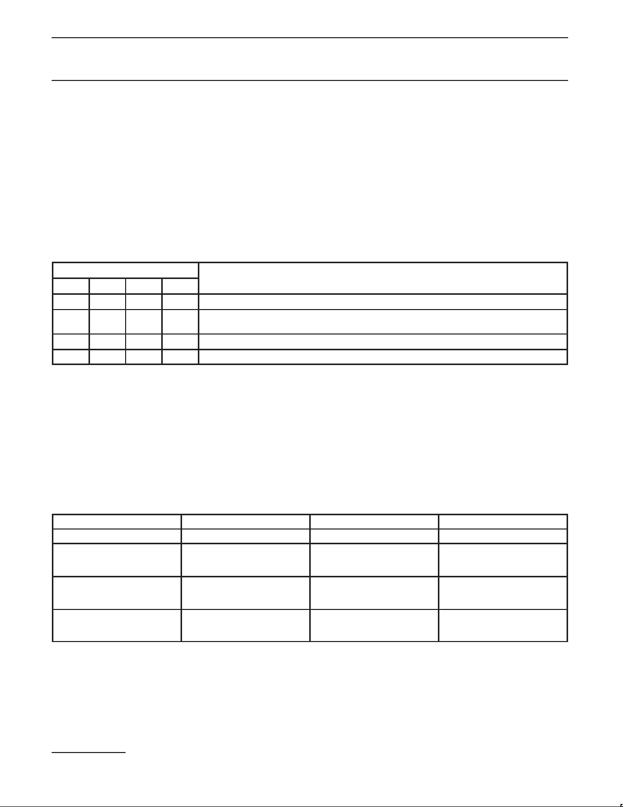
Philips Semiconductors Product specification
XA 16-bit microcontroller family
XA-G3
32K/512 OTP/ROM/ROMless, watchdog, 2 UARTs
EPROM CHARACTERISTICS
The XA-G37 is programmed by using a modified Improved
Quick-Pulse Programming algorithm. This algorithm is essentially
the same as that used by the later 80C51 family EPROM parts.
However different pins are used for many programming functions.
Detailed EPROM programming information may be obtained from
the internet at www.philipsmcu.com/ftp.html.
The XA-G3 contains three signature bytes that can be read and
used by an EPROM programming system to identify the device. The
signature bytes identify the device as an XA-Gx manufactured by
Philips.
Table 6. Program Security Bits
PROGRAM LOCK BITS
SB1 SB2 SB3 PROTECTION DESCRIPTION
1 U U U No Program Security features enabled.
2 P U U MOVC instructions executed from external program memory are disabled from fetching code bytes
from internal memory and further programming of the EPROM is disabled.
3 P P U Same as 2, also verify is disabled.
4 P P P Same as 3, external execution is disabled. Internal data RAM is not accessible.
NOTES:
1. P – programmed. U – unprogrammed.
2. Any other combination of the security bits is not defined.
Security Bits
With none of the security bits programmed the code in the program
memory can be verified. When only security bit 1 (see Table 6) is
programmed, MOVC instructions executed from external program
memory are disabled from fetching code bytes from the internal
memory. All further programming of the EPROM is disabled. When
security bits 1 and 2 are programmed, in addition to the above,
verify mode is disabled. When all three security bits are
programmed, all of the conditions above apply and all external
program memory execution is disabled. (See Table 6)
ROM CODE SUBMISSION
When submitting ROM code for the XA-G33, the following must be specified:
1. 32k bytes user ROM data.
2. ROM security bits.
ADDRESS CONTENT BIT(S) COMMENT
0000H to 7FFFH DATA 7:0 User ROM Data
8020H SECURITY BIT 0 ROM Security Bit 1
8020H SECURITY BIT 1 ROM Security Bit 2
8020H SECURITY BIT 3 ROM Security Bit 3
Trademark phrase of Intel Corporation.
0 = enable security
1 = disable security
0 = enable security
1 = disable security
0 = enable security
1 = disable security
1999 Apr 07
32
Page 33
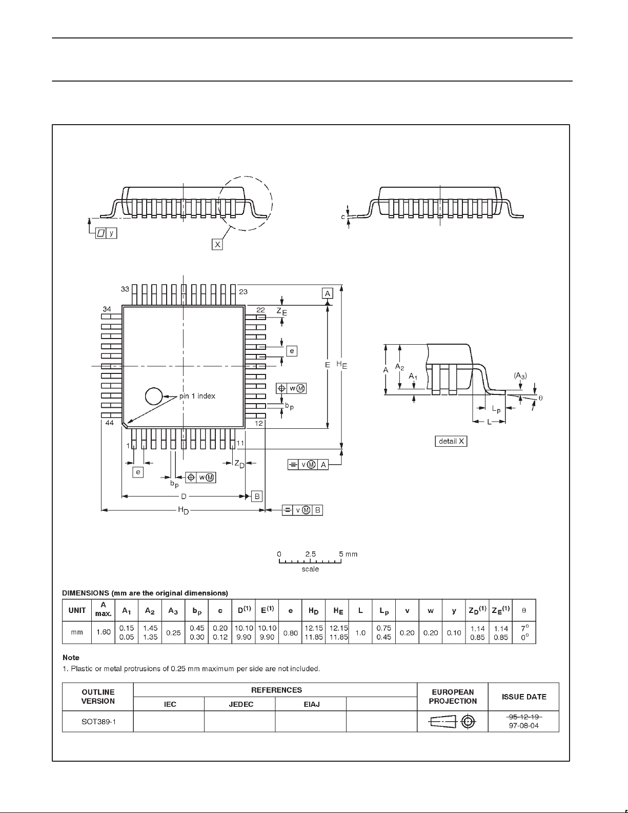
Philips Semiconductors Product specification
XA 16-bit microcontroller family
XA-G3
32K/512 OTP/ROM/ROMless, watchdog, 2 UARTs
LQFP44: plastic low profile quad flat package; 44 leads; body 10 x 10 x 1.4 mm SOT389-1
1999 Apr 07
33
Page 34
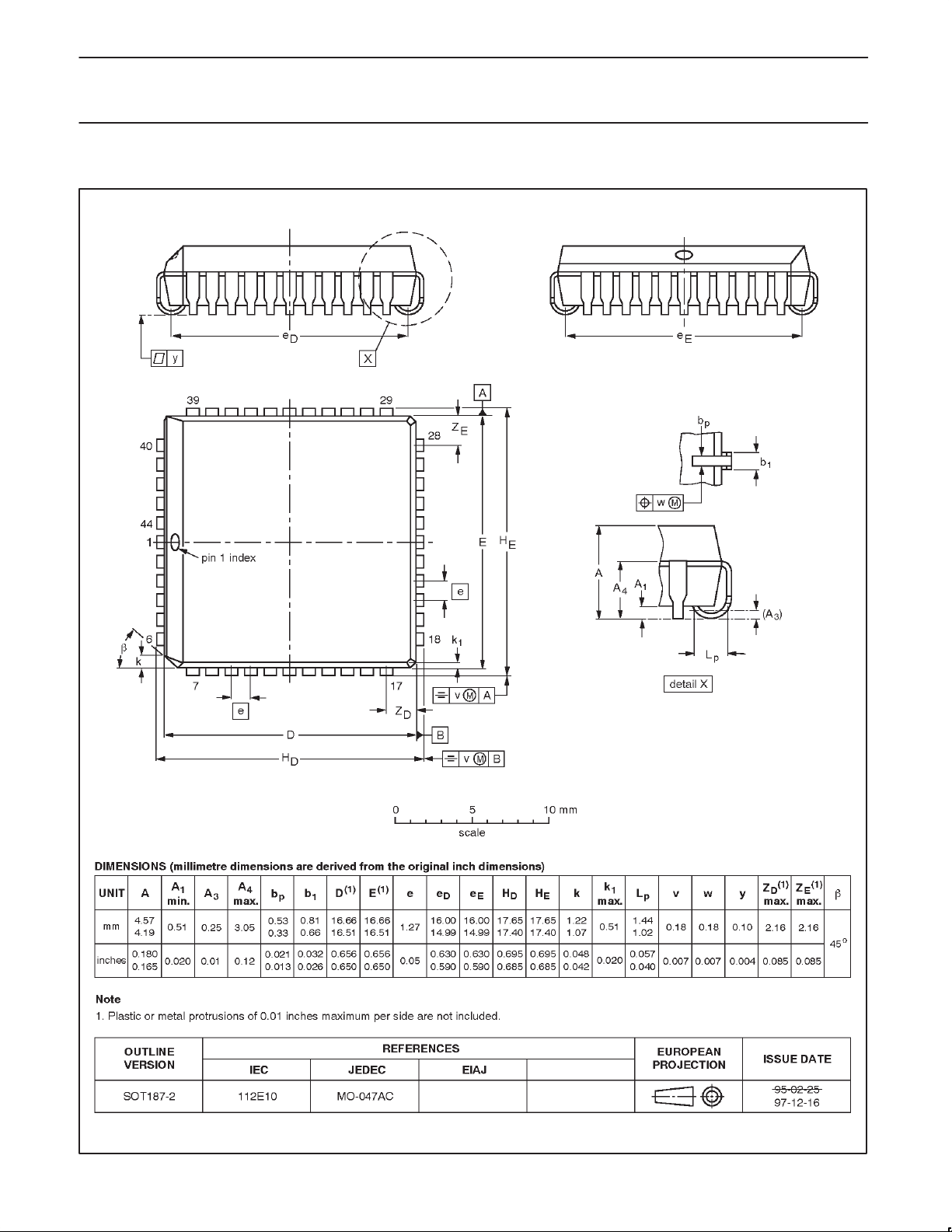
Philips Semiconductors Product specification
XA 16-bit microcontroller family
XA-G3
32K/512 OTP/ROM/ROMless, watchdog, 2 UARTs
PLCC44: plastic leaded chip carrier; 44 leads SOT187-2
1999 Apr 07
34
Page 35

Philips Semiconductors Product specification
XA 16-bit microcontroller family
32K/512 OTP/ROM/ROMless, watchdog, 2 UARTs
NOTES
XA-G3
1999 Apr 07
35
Page 36

Philips Semiconductors Product specification
XA 16-bit microcontroller family
32K/512 OTP/ROM/ROMless, watchdog, 2 UARTs
Data sheet status
Data sheet
status
Objective
specification
Preliminary
specification
Product
specification
Product
status
Development
Qualification
Production
Definition
This data sheet contains the design target or goal specifications for product development.
Specification may change in any manner without notice.
This data sheet contains preliminary data, and supplementary data will be published at a later date.
Philips Semiconductors reserves the right to make chages at any time without notice in order to
improve design and supply the best possible product.
This data sheet contains final specifications. Philips Semiconductors reserves the right to make
changes at any time without notice in order to improve design and supply the best possible product.
[1]
XA-G3
[1] Please consult the most recently issued datasheet before initiating or completing a design.
Definitions
Short-form specification — The data in a short-form specification is extracted from a full data sheet with the same type number and title. For
detailed information see the relevant data sheet or data handbook.
Limiting values definition — Limiting values given are in accordance with the Absolute Maximum Rating System (IEC 134). Stress above one
or more of the limiting values may cause permanent damage to the device. These are stress ratings only and operation of the device at these or
at any other conditions above those given in the Characteristics sections of the specification is not implied. Exposure to limiting values for extended
periods may affect device reliability.
Application information — Applications that are described herein for any of these products are for illustrative purposes only. Philips
Semiconductors make no representation or warranty that such applications will be suitable for the specified use without further testing or
modification.
Disclaimers
Life support — These products are not designed for use in life support appliances, devices or systems where malfunction of these products can
reasonably be expected to result in personal injury . Philips Semiconductors customers using or selling these products for use in such applications
do so at their own risk and agree to fully indemnify Philips Semiconductors for any damages resulting from such application.
Right to make changes — Philips Semiconductors reserves the right to make changes, without notice, in the products, including circuits, standard
cells, and/or software, described or contained herein in order to improve design and/or performance. Philips Semiconductors assumes no
responsibility or liability for the use of any of these products, conveys no license or title under any patent, copyright, or mask work right to these
products, and makes no representations or warranties that these products are free from patent, copyright, or mask work right infringement, unless
otherwise specified.
Philips Semiconductors
811 East Arques Avenue
P.O. Box 3409
Sunnyvale, California 94088–3409
Telephone 800-234-7381
Copyright Philips Electronics North America Corporation 1999
All rights reserved. Printed in U.S.A.
Date of release: 04-99
Document order number: 9397 750 05538
1999 Apr 07
36
 Loading...