

Page 1
WM9703
AC’97 Revision 2.1 Audio Codec
Production Data, January 2001, Rev 3.4
DESCRIPTION
WM9703 is a high-quality s tereo audio codec compliant
with the AC’97 Revision 2.1 specificati on. It performs full
duplex 18-bit codec functions and supports variable
sample rates from 8 to 48k sam pl es/ s and of fers excellent
quality with high SNR. Additional features include 3D
sound and line-level outputs. In addition, support is
provided for variable sample rates and accom modation is
made for master/ slave mode operation.
WM9703 is interchangeable with AC’97 codecs from
Wolfson and other suppliers. The WM9703 is fully
operable on 3.3V or 5V or mixed 3.3/5V supplies, and is
packaged in the industry standard 48-pin TQFP package
with 7mm-body size.
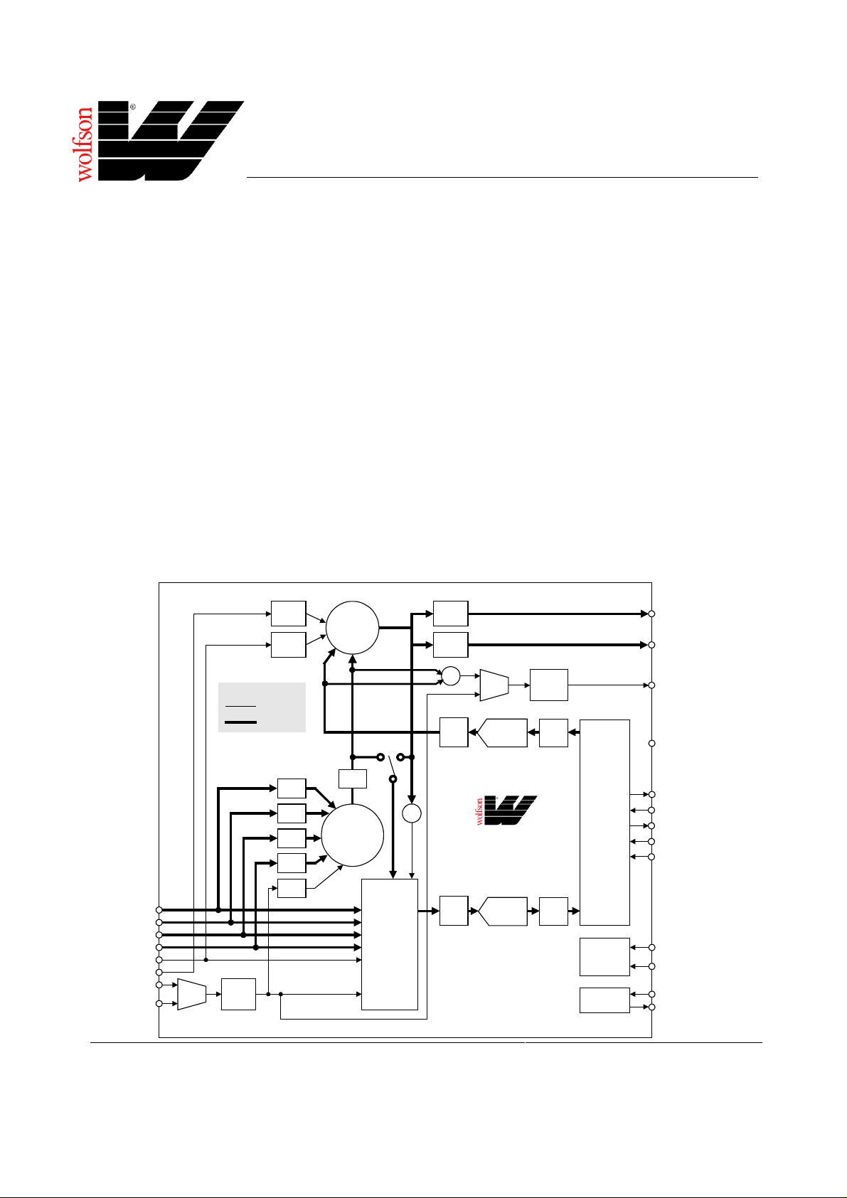
BLOCK DIAGRAM
VOL/
MUTE
VOL/
MUTE
Σ
AC’97 FEATURES
• 3.3V or 5V operation
• 18-bit stereo codec
• S/N ratio > 95dB
• Multiple stereo input mixer
• Mono and stereo volume control
• 48-pin TQFP package
• Power management features
• Low power implementation
• Very low standby power
AC’97 REVISION 2.1 FEATURES
• Variable rate audio (VRA) support
• Analogue 3D stereo enhancement
• Line level outputs
• Supports Revision. 2.1 s pecified modem sample rates
and filtering
• Master/slave ID selection
• PC-beep connection when device held reset
VOL/
MUTE
VOL/
MUTE
(35,36) LINEOUT
(39,41) LNLVLOUT
KEY:
MONO
STEREO
3D
Σ
CD (18,20)
LINEIN (23,24)
VIDEO (16,17)
AUX ( 14,15)
PHONE (13)
PCBEEP (12)
MIC[1] (2 1)
MIC[2] (2 2)
MUX
0dB/
20dB
VOL/
MUTE
VOL/
MUTE
VOL/
MUTE
VOL/
MUTE
VOL/
MUTE
WOLFSON MICROELECTRONICS LTD
Lutton Court, Bernard Terrace, Edi nburgh, EH8 9NX, UK
Tel: +44 (0) 131 667 9386
Fax: +44 (0) 131 667 5176Email: [email protected]
http://www.wolfson.co.uk
RECORD
MUX
AND
MUTE
Σ
MUX
STEREO
VOL
DAC
Σ
WM9703
VOL
STEREO
ADC
VOL/
MUTE
SRC
SRC
SERIAL
I/F
MASTER/
SLAVE
SELECT
OSC
(37) MONOOUT
(47) EAPD
(6) BITCLK
(10) SYNC
(8) SDATAIN
(5) SDATAOUT
(11) RESETB
(45) CID[0]
(46) CID[1]
(2) XTLIN
(3) XTLOUT
Production Data datasheets contain final
specifications current on publication date.
Supply of products conforms to Wol fson
Microelectronics’ Term s and Conditions.
2001 Wolfson Microelectronics Ltd.
Page 2
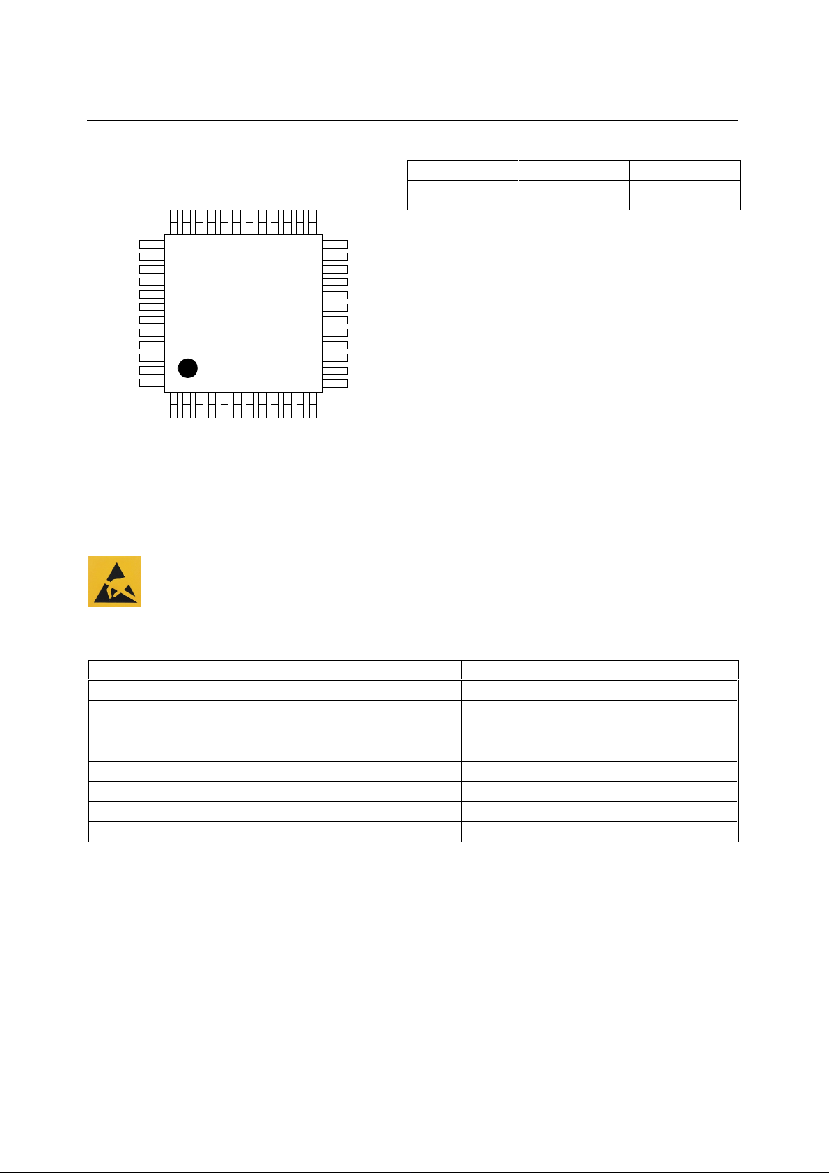
WM9703 Production Data PIN CONFIGURATION ORDERING INFORMATION
DEVICE TEMP. RANGE PACKAGE
WM9703CFT/V 0 to 70oC 48-pin TQFP
MONOOUT
AVDD2
LNLVLOUTL
LNLVLOUTR
AVSS2
CID0
CID1
EAPD
LINEOUTR
CX3D2
LINEOUTL
3635343332
37
38
39
40
NC
41
42
43
NC
44
NC
45
46
47
48
NC
1
DVDD1
3
2
XTLIN
XTLOUT
CAP1
CAP2
CX3D1
3130292827
WM9703
6
5
4
DVSS1
BITCLK
SDATAOUT
NC
7
DVSS2
AVDD1
AVSS1
VREF
VREFOUT
AFILT1
25
26
24
LINEINR
23
LINEINL
MIC2
22
21
MIC1
20
CDR
19
CDGND
18
CDL
VIDEOR
17
16
VIDEOL
15
AUXR
AUXL
14
PHONE
13
9
8
SDATIN
DVDD2
10
SYNC
11
RESETB
12
PCBEEP
ABSOLUTE MAXIMUM RATINGS
Absolute Maximum Ratings are stress rati ngs only. Permanent damage to the devic e may be caus ed by conti nuously operating
at or beyond these limits . Devi ce f unct ional operat ing li m it s and guarant eed perform anc e spec if ic ations are given under E lect ri cal
Characteristics at the test conditions s pecified.
ESD Sensitive Device. Thi s devi ce is m anufac tu red on a CMOS proces s. It is t herefore generic ally sus c eptibl e
to damage from excessive static voltages . Proper ES D precaut ions m ust be tak en during handli ng and st orage
of this device.
As per specifications IPC/JEDEC J-STD-020A and JEDEC A113-B, this product requires specific storage conditions prior to
surface mount assembly. It has been classified as having a Moisture Sensitivity Level of 2 and as such will be supplied in
vacuum-sealed moisture barrier bags.
CONDITION MIN MAX
Digital supply voltage
Analogue supply voltage
Voltage range digital inputs
Voltage range analogue inputs
Operating temperature range, T
A
Storage temperature
Package body temperature (s ol deri ng 10 seconds)
Package body temperature (s ol deri ng 2 minutes)
-0.3V +7V
-0.3V +7V
DVSS
-0.3V DVDD +0.3V
AVDD
-0.3V AVDD +0.3V
0oC+70
o
-65
C +150oC
+240
+183
o
C
o
C
o
C
Note:
1. The digital supply voltage (DVDD) must always be less than or equal to the analogue supply voltage (AVDD).
WOLFSON MICROELECTRONICS LTD PD Rev 3.4 January 2001
2
Page 3
Production Data WM9703
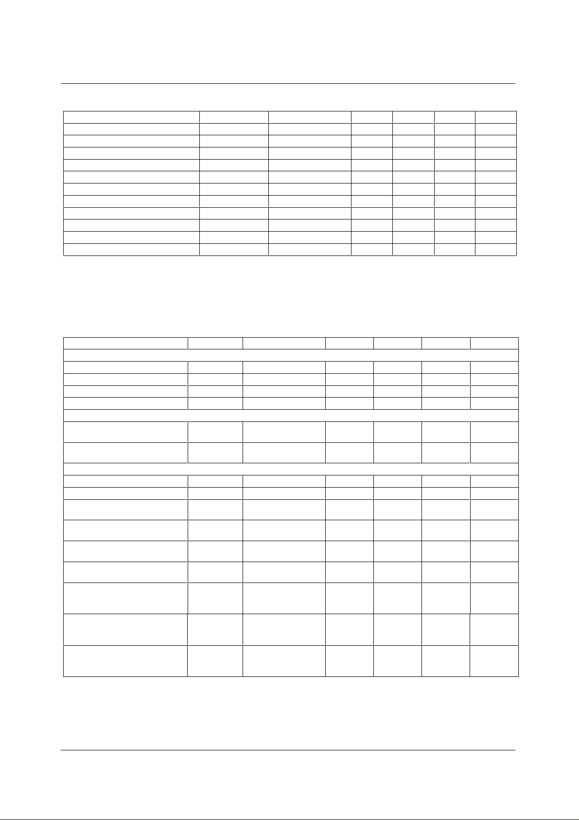
RECOMMENDED OPERATING CONDITIONS
PARAMETER SYMBOL TEST CONDITIONS MIN TYP MAX UNIT
Digital supply range
Analogue supply range
Digital ground
Analogue ground
Difference DVSS to AVSS
Analogue supply current
Digital supply current
Standby supply current (all P Rs set)
Analogue supply current
Digital supply current
Standby supply current (all P Rs set)
DVDD1, DVDD2 -10% 3.3 to 5.0 +10% V
AVDD1, AVDD2 -10% 3.3 to 5.0 +10% V
DVSS1, DVSS2 0 V
AVSS1, AVSS2 0 V
-0.3 0 +0.3 V
DVDD, AVDD = 5V 35 mA
DVDD, AVDD = 5V 25 mA
DVDD, AVDD = 5V 10 µA
DVDD, AVDD = 3.3V 22 mA
DVDD, AVDD = 3.3V 15 mA
DVDD, AVDD = 3.3V 6 µA
ELECTRICAL CHARACTERISTICS
Test Characteristics:
AVDD = 5V, GND = 0V …………..T
DVDD = 3.3V, GND = 0V …………..T
= 0oC to +70oC, unless otherwise stated
A
= 0oC to +70oC, unless otherwise stated
A
PARAMETER SYMBOL TEST CONDITIONS MIN TYP MAX UNIT
Digital Logic Levels (DVDD = 3.3 or 5.0V)
Input LOW level V
Input HIGH level V
Output LOW V
Output HIGH V
IL
IH
OL
OH
AVSS -0.3 0.8 V
2.2 AVDD +0.3 V
0.1 x DVDD V
0.9 x DVDD V
Analogue I/O Levels (Input Signals on any inputs, Outputs on LINEOUT L, R and MONOOUT)
Input level
Output level
Minimum input
impedance = 10k
AVSS
-100mV
Into 10kohm load AVSS
+100mV
Near rail to
rail
AVDD
+100mV
AVDD
-100mV
V
V
Reference Levels
Reference input/output CAP2
CAP2 impedance
Mixer reference VREF
2/5 AVDD AVDD/2 3/5 AVDD V
75 kohms
Buffered
V
CAP2
MIC reference VREFOUT
Buffered
V
CAP2
ADC reference CAP1
Buffered
V
CAP2
DAC reference AFILT1
Buffered
V
CAP2
MIDBUFF current sink
AVDD = 5V -5 -15 mA
(pins CAP1, AFILT2, VREF
and VREFOUT)
MIDBUFF current source
AVDD = 5V 5 15 mA
(pins CAP1, AFILT1, VREF
and VREFOUT)
MIDBUFF current source
AVDD = 3.3V 5 mA
(pins CAP1, AFILT1, VREF
and VREFOUT)
WOLFSON MICROELECTRONICS LTD PD Rev 3.4 January 2001
3
Page 4
WM9703 Production Data
Test Characteristics:
AVDD = 5V, GND = 0V …………..T
DVDD = 3.3V, GND = 0V …………..T
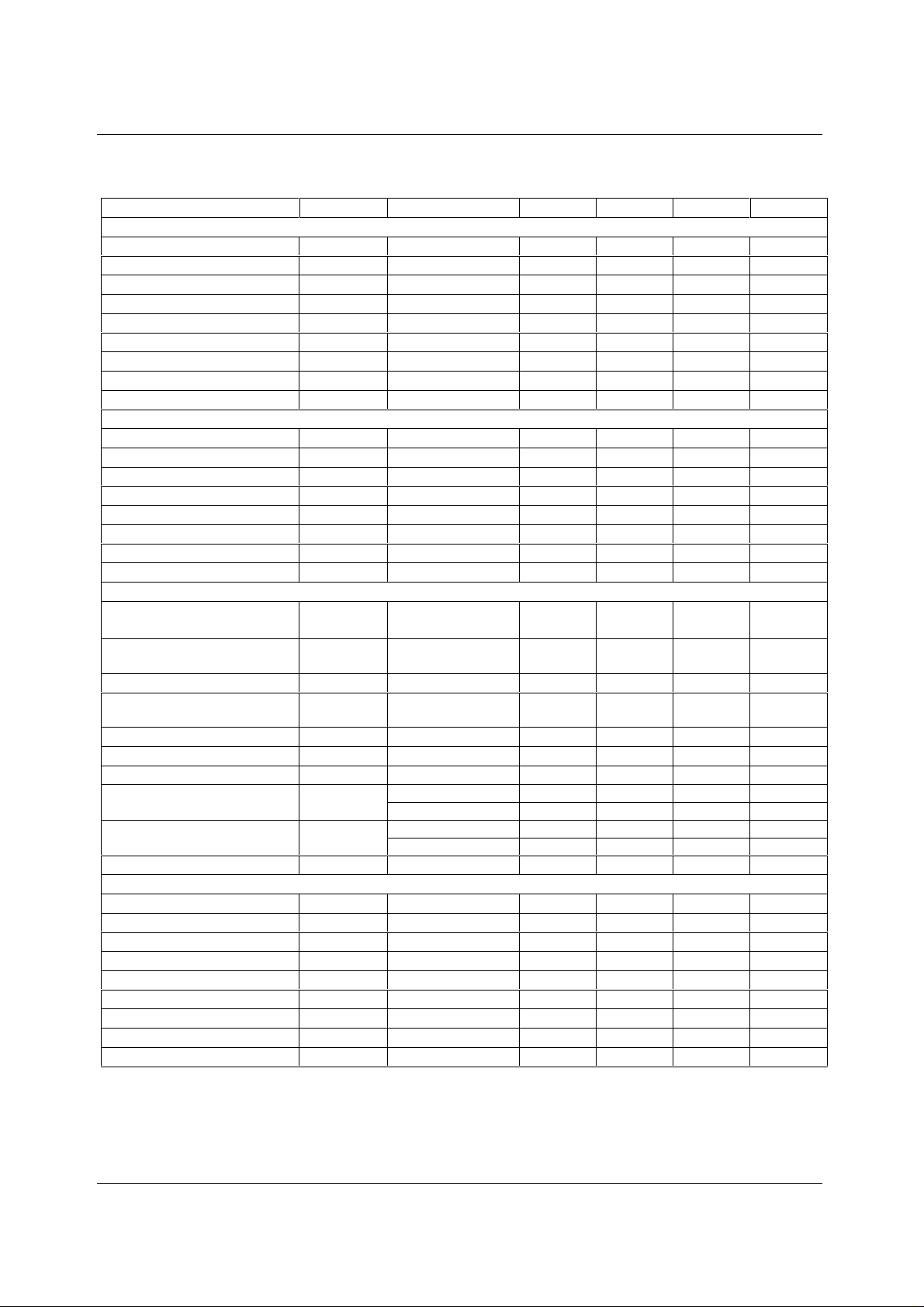
PARAMETER SYMBOL TEST CONDITIONS MIN TYP MAX UNIT
DAC Circuit Specifications (AVDD = 5V) 48kHz sampling
SNR A-weighted (Note 1)
Full scale output voltage
THD
Frequency response
Transition band
Stop band
Out of band rejection
Spurious tone reduction
PSRR
ADC Circuit Specifications (AVDD = 5V) 48kHz sampling
SNR A-weighted (Note 1)
ADC input for full scal e out put
THD
Frequency response
Transition band
Stop band
Stop band rejection
PSRR
Mixer Circuit Specificati ons (AVDD = 5V) 48kHz sampling
SNR CD path A-weighted
(Note 1)
SNR Other paths A-weighted
(Note 1)
Maximum input voltage
Maximum output voltage on
LINEOUT
THD
Frequency response (+/-1dB)
Input impedance (CD inputs )
Input impedance (other mixer
inputs)
Input impedance Mic inputs
PSRR
DAC Circuit Specifications (AVDD = 3.3V) 48kHz sampling
SNR A-weighted (Note 1)
Full scale output voltage
THD
Frequency response
Transition band
Stop band
Out of band rejection
Spurious tone reduction
PSRR
= 0oC to +70oC, unless otherwise stated
A
= 0oC to +70oC, unless otherwise stated
A
VREF
= 2.5V 1.0 Vrms
-3dBFs input 74 90 dB
20 to 20kHz 40 dB
VREF
= 2.5V 1.0 Vrms
-6dBV input 74 90 dB
20 to 20kHz 40 dB
0dBV input 74 90 dB
At any gain 10 15 kohm
At max gain 10 20 kohm
At 0db gain 100 kohm
At max gain 80 kohm
At 0db gain 10 15 kohm
20 to 20kHz 40 dB
VREF
= 1.65V 0.7 Vrms
3dBFs input 90 dB
20 to 20kHz 40 dB
85 96 dB
20 19,200 Hz
19,200 28,800 Hz
28,800 Hz
-40 dB
-100 dB
75 85 dB
20 19,200 Hz
19,200 28,800 Hz
28,800 Hz
-74 dB
90 100 dB
85 95 dB
AVSS 1.0 AVDD Vrms
1.0 1.8 Vrms
20 20,000 Hz
96 dB
20 19,200 Hz
19,200 28,800 Hz
28,800 Hz
-40 dB
-100 dB
WOLFSON MICROELECTRONICS LTD PD Rev 3.4 January 2001
4
Page 5

Production Data WM9703
Test Characteristics:
AVDD = 5V, GND = 0V …………..T
DVDD = 3.3V, GND = 0V …………..T
= 0oC to +70oC, unless otherwise stated
A
= 0oC to +70oC, unless otherwise stated
A
PARAMETER SYMBOL TEST CONDITIONS MIN TYP MAX UNIT
ADC Circuit Specifications (AVDD = 3.3V) 48kHz sampling
SNR A-weighted (Note 1)
ADC input for full scal e out put
THD
Frequency response
Transition band
Stop band
Stop band rejection
PSRR
VREF
= 1.65V 0.7 Vrms
-9dBV input 80 dB
20 19,200 Hz
19,200 28,800 Hz
28,800 Hz
-74 dB
20 to 20kHz 40 dB
82 dB
Mixer Circuit Specificati ons (AVDD = 3.3V) 48kHz sampling
SNR CD path A-weighted
97 dB
(Note 1)
SNR Other paths A-weighted
92 dB
(Note 1)
Maximum input voltage
Maximum output voltage on
0.7 Vrms
0.7 Vrms
LINEOUT
THD
Frequency response (+/-1dB)
Input impedance (CD inputs )
Input impedance (other Mixer
inputs)
Input impedance MIC inputs
-3dBV input 90 dB
20 20,000 Hz
At any gain 15 kohm
At max gain 20 kohm
At 0db gain 100 kohm
At max gain 80 kohm
At 0db gain 15 k ohm
PSRR
20 to 20kHz 40 dB
Clock Frequency Range
Crystal clock
BIT_CLK frequency
SYNC frequency
24.576 MHz
12.288 MHz
48.0 kHz
Note:
1. SNR is the ratio of 0dB signal output level to the output level with no signal, measured A-weighted over a 20Hz t o 20kHz
bandwidth.
WOLFSON MICROELECTRONICS LTD PD Rev 3.4 January 2001
5
Page 6

WM9703 Production Data PIN DESCRIPTION
PIN NAME TYPE DESCRIPTION
1
2
3
4
5
6
7
8
9
10
11
12
13
14
15
16
17
18
19
20
21
22
23
24
25
26
27
28
29
30
31
32
33
34
35
36
37
38
39
40
41
42
43
44
45
46
47
48
Note:
1 Pins 27, 29 and 31 have an internal connection.
WOLFSON MICROELECTRONICS LTD PD Rev 3.4 January 2001
DVDD1 Supply Digital positive supply
XTLIN Digital input Clock crystal connection or clock input (XTAL not used)
XTLOUT Digital output Clock crystal connection
DVSS1 Supply Digital ground supply
SDATAOUT Digital i nput Serial data input
BITCLK Digi tal output (master)
Digital input (slave)
DVSS2 Supply Digital ground supply
SDATAIN Digital output Serial data output to AC’97 controller
DVDD2 Supply Digital positive supply
SYNC Digital input Serial interfac e sync pulse from AC’97 control l er
RESETB Digital input NOT reset input (ac tive low, resets registers)
PCBEEP Analogue input Mixer input, typically for PCBEEP signal
PHONE Analogue input Mixer input, typically for PHONE signal
AUXL Analogue input Mixer input, typically for AUX signal
AUXR Analogue input Mixer input, typically for AUX signal
VIDEOL Analogue input Mixer input, typically for VIDEO signal
VIDEOR Analogue input Mixer input, typically for VI DE O signal
CDL Analogue input Mixer input, typically for CD signal
CDGND Analogue input CD input common mode reference (ground)
CDR Analogue input Mixer input, typically for CD signal
MIC1 Analogue input Mixer input with extra gain if required
MIC2 Analogue input Mixer input with extra gain if required
LINEINL Analogue input Mixer input, typically for LINE signal
LINEINR Analogue input Mixer input, typically for LINE signal
AVDD1 Suppl y Analogue positive supply
AVSS1 Supply Analogue ground supply, chip substrate
VREF( note1) Analogue output Buffered CAP2
VREFOUT Analogue output Reference for microphones; buffered CAP2
AFILT1( note1) Analogue output Buffered CAP2
NC No internal connection
CAP1(note 1) Analogue output Buffered CAP2
CAP2 Analogue i nput Reference input/output; pulls to midrai l i f not driven
CX3D1 Analogue output Output pin for 3D difference s i gnal
CX3D2 Analogue input I nput pin for 3D difference signal
LINEOUTL Analogue output Main analogue output f or l ef t channel
LINEOUTR Analogue output Main anal ogue out put for right channel
MONOOUT Analogue output Main mono output
AVDD2 Suppl y Analogue positive supply
LNLVLOUTL Anal ogue output Left channel line l evel output
NC No internal connection
LNLVLOUTR Analogue output Right channel line l evel output
AVSS2 Supply Analogue ground supply, chip substrate
NC No internal connection
NC No internal connection
CID0 Digital i nput Master/slave ID selec t (internal pull-up)
CID1 Digital i nput Master/slave ID selec t (internal pull-up)
EAPD Digital output External amplifier powerdown/GPO
NC No internal connection
Serial interface cloc k output to AC’97 controller
or input from AC’97 mas ter codec
6
Page 7
Production Data WM9703
DETAILED TIMING DIAGRAMS
Test Characteristics:
AVDD = 5V, GND = 0V …………..T
DVDD = 3.3V, GND = 0V …………..T
All measurement s are taken at 10% to 90% VDD, unl ess otherwise stated.
AC-LINK LOW POWER MODE
= 0oC to +70oC, unless otherwise stated.
A
= 0oC to +70oC, unless otherwise stated.
A
COLD RESET
SYNC
SLOT 1 SLOT 2
BIT_CLK
SDATA_OUT
WRITE
TO 0X20
DATA PR4
t
S2_PDOWN
DON’T
CARE
SDATA_IN
Figure 1 AC-Link Powerdown Timing
PARAMETER SYMBOL MIN TYP MAX UNIT
End of slot 2 to BITCLK S DA T IN
t
S2_PDOWN
1.0 µs
low
t
RST_LOW
t
RST2CLK
RESETB
BIT_CLK
Figure 2 Cold Reset Timing
PARAMETER SYMBOL MIN TYP MAX UNIT
RESETB active low pulse width t
RESETB inactive to BIT_CLK
RST_LOW
t
RST2_CLK
1.0 µs
162.8 ns
start-up delay
WOLFSON MICROELECTRONICS LTD PD Rev 3.4 January 2001
7
Page 8
WM9703 Production Data
WARM RESET
Figure 3 Warm Reset Timing
SYNC active high pulse width t
SYNC inactive to BIT_CLK start-
up delay
CLOCK SPECIFICATIONS
t
SYNC_HIGH
t
SYNC2CLK
SYNC
BIT_CLK
PARAMETER SYMBOL MIN TY P MAX UNIT
1.3 µs
BIT_CLK
t
CLK_HIGH
t
CLK_PERIOD
t
SYNC_HIGH
SYNC_HIGH
t
SYNC2_CLK
162.4 ns
t
CLK_LOW
t
SYNC_LOW
SYNC
t
SYNC_PERIOD
Figure 4 Clock Specifications (50pF External Load)
Note: Worst case duty cycle restricted to 40/60.
PARAMETER SYMBOL MIN TYP MAX UNIT
BIT_CLK frequency
BIT_CLK period t
BIT_CLK output jitter
BIT_CLK high pulse width (Note 1) t
BIT_CLK low pulse width (Note 1) t
SYNC frequency
SYNC period t
SYNC high pulse width t
SYNC low pulse width t
CLK_PERIOD
CLK_HIGH
CLK_LOW
SYNC_PERIOD
SYNC_HIGH
SYNC_LOW
32.56 40.7 48.84 ns
32.56 40.7 48.84 ns
12.288 MHz
81.4 ns
750 ps
48.0 kHz
20.8 µs
1.3 µs
19.5 µs
WOLFSON MICROELECTRONICS LTD PD Rev 3.4 January 2001
8
Page 9
Production Data WM9703
DATA SETUP AND HOLD (50PF EXTERNAL LOAD)
t
SETUP
BIT_CLK
t
HOLD
SYNC
SDATA_OUT
Figure 5 Data Setup and Hold (50pF External Load)
Note: Setup and hold time parameters for SDATA_IN are with respect to AC’97 Controller.
PARAMETER SYMBOL MIN TYP MAX UNIT
Setup to falling edge of BIT_CLK t
Hold from falling edge of BI T_CLK t
SETUP
HOLD
15.0 ns
5.0 ns
SIGNAL RISE AND FALL TIMES
t
BIT_CLK
t
rise
rise
CLK
SYNC
t
fall
CLK
t
fall
SYNC
SYNC
t
rise
DIN
t
fall
DIN
SDATA_IN
t
rise
DOUT
t
fall
DOUT
SDATA_OUT
Figure 6 Signal Rise and Fall Times (50pF External Load)
PARAMETER SYMBOL MIN TYP MAX UNIT
BIT_CLK rise time trise
BIT_CLK fall time tfall
SYNC rise time trise
SYNC fall time tfall
SDATA_IN rise time trise
SDATA_IN fall time trise
SDATA_OUT rise time trise
SDATA_OUT fall time tfall
CLK
CLK
SYNC
SYNC
DIN
DIN
DOUT
DOUT
26ns
26ns
26ns
26ns
26ns
26ns
26ns
26ns
WOLFSON MICROELECTRONICS LTD PD Rev 3.4 January 2001
9
Page 10
WM9703 Production Data
SYSTEM INFORMATION
CD, VIDEO,
AUX, LINEINL/
R
MIC2
MIC1
PCBEEP PHONE
AC’97
DIGITAL
CONTROLLER
CHIP
SELECT
RESET
BITCL
K
SYNC
SDATAI
N
SDATAOU
T
CID0
CID1
{
11
6
10
8
5
45
46
WM9703
Figure 8 Revision 2.1 Compliant 2-Channel Codec
SDATAOUT
SDATAIN
PC I/O
CHIPSET
OR AC’97
CONTROLLER
BITCLK
SYNC
RESET
SDATAOUT
BITCLK
SDATAIN
SYNC
RESET
XTLOUT
13122122
LINEOUTL
WM9703
LINEOUTR
ID=00
35
36
39
41
37
LINEOUTL/R
{
LNLVLOUTL/R
MONOOUT
Front R data
Front L data
XTLIN
SDATAOUT
BITCLK
SDATAIN
SYNC
RESET
LINEOUTL
WM9703
LINEOUTR
ID=10
Surround R data
Surround L data
Figure 9 WM9703 in a 4 Channel S ystem
WOLFSON MICROELECTRONICS LTD PD Rev 3.4 January 2001
10
Page 11
Production Data WM9703
SDATAOUT
SDATAIN
PC I/O
CHIPSET
OR AC’97
CONTROLLER
BITCLK
SYNC
RESET
SDATAOUT
BITCLK
SDATAIN
SYNC
RESET
XTLOUT
XTLIN
SDATAOUT
BITCLK
SDATAIN
SYNC
RESET
XTLIN
SDATAOUT
BITCLK
SDATAIN
SYNC
RESET
WM9703
WM9703
WM9703
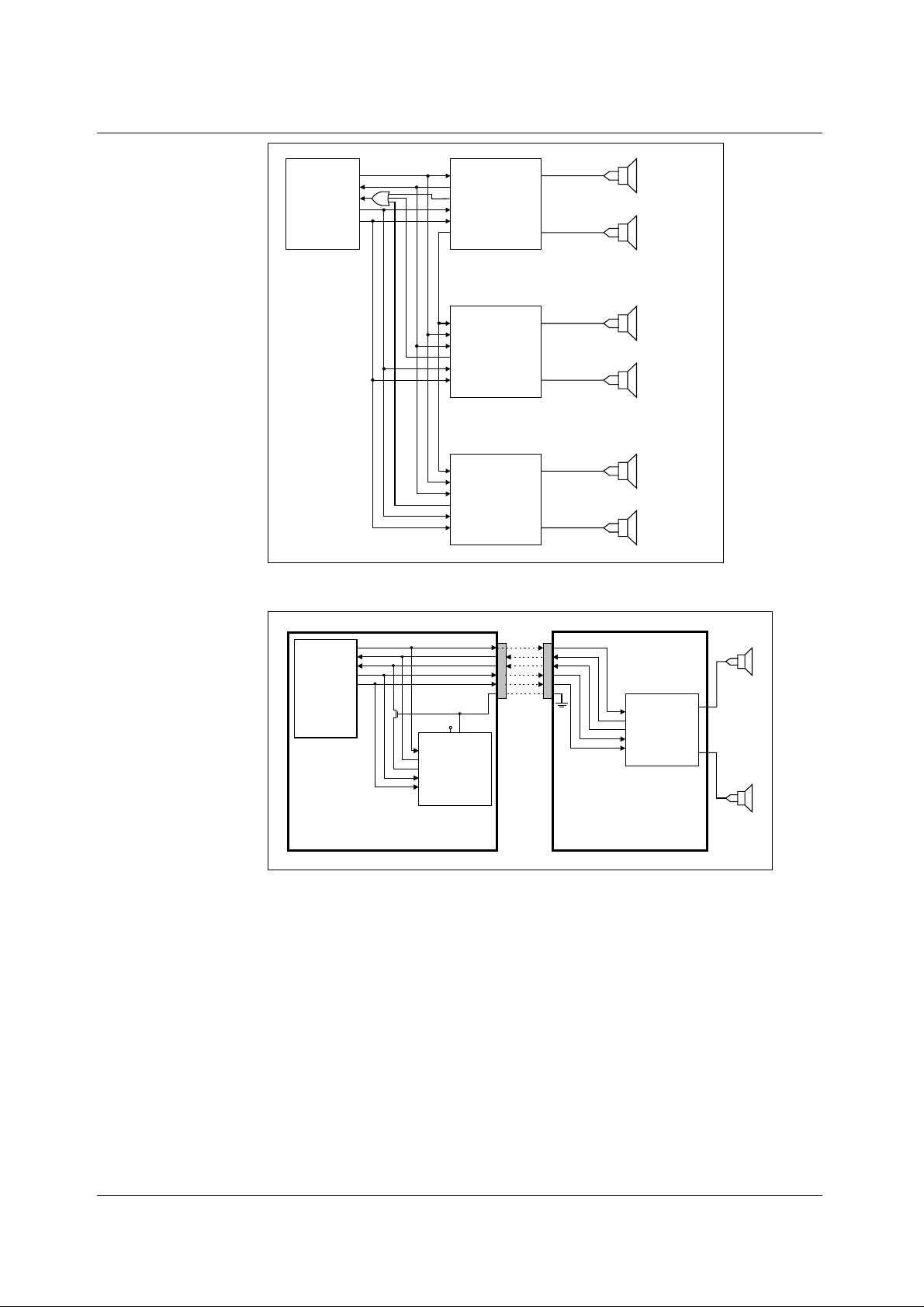
Figure 10 WM9703 in a 6 Channel S ystem
LINEOUTL
LINEOUTR
ID=00
LINEOUTL
LINEOUTR
ID=10
LINEOUTL
LINEOUTR
ID=11
Front R data
Front L data
Surround R data
Surround L data
Centre data
LFE data
SDATAOUT
BITCLK
SDATAIN
SYNC
RESETB
PC I/O
CHIPSET
OR AC’97
CONTROLLER
Option of using RESETB
or SDATAIN to disable
NB CODEC
when docked.
CID1CID0
SDATAOUT
BITCLK
SDATAIN
WM9703
SYNC
RESETB
ID=00
If pins CID0/1 not
driven then CODEC ID
NOTEBOOK/
LAPTOP
defaults to 00.
When docked CID1 is
pulled low making
CODEC a ’slave’ (01)
stopping BITCLK
Figure 11 WM9703 in a Docking Stati on System
SDATAOUT
BITCLK
SDATAIN
WM9703
SYNC
RESETB
DOCKING STATION
LINEOUTL
LINEOUTR
ID=00
WOLFSON MICROELECTRONICS LTD PD Rev 3.4 January 2001
11
Page 12

WM9703 Production Data DEVICE DESCRIPTION
INTRODUCTION
The WM9703 is fully c ompliant with Revision 2.1 of t he A C’97 specification.
The WM9703 comprises a stereo 18-bit Codec , (that is, 2 A DCs and 2 DACs) pl us a com prehensive
analogue mixer with 4 sets of stereo inputs, plus phone, 2 microphone, and PC-beep inputs.
Additionally, on-chip reference generation circuits generate the necessary bias voltages for the
device, and a bidirectional s erial i nterf ace all ows transf er of c ontrol dat a and DA C and ADC words to
and from the AC’97 controller. The W M9703 supports 18-bit resolution within the DAC and ADC
functions, but the AC’97 serial interface specification allows any word length up to 20-bits to be
written to, or read from, the A C’97 Codec. These words are MSB justified, and any LS Bs not used
will simply default to 0. Normally it is anticipated that 16-bit words will be used in most PC type
systems. Therefore, for the DAC, 16-bit words will be downloaded into the Codec from the controller,
along with padding of 0s to make the 16-bit word up to 20-bit length. In this cas e, the WM9703 will
process the 16-bit word along with 0 padding bits in the 2 LSB loc ations (to m ak e 18-bit ). A t the A DC
output, WM9703 will provide an 18-bit word, again with 0s in the two LSB locations (20-bit). The
AC’97 controller will then ignore the 4 LSBs of the 20-bit word. When the WM9703 is interrogated, it
responds indicating it i s an 18-bit device.
The WM9703 has the ADC and DAC functions implemented using oversampled, or sigma-delta
converters, and uses on-chip digital filters to convert these 1-bit signals to and from the 48ks/s
16/18-bit PCM words that the AC’97 controll er requires. The digital parts of the device are powered
separately from the analogue to optimise performance and 3.3V digital and 5V analogue supplies
may be used on the same device to f urther optimise perform ance. Digital I Os are 5V tolerant when
the analogue supplies are 5V, so the WM9703 may be connected to a controller running on 5V
supplies, but use 3.3V for the digital section of WM9703. WM9703 is al so capable of operating with a
3.3V supply only (digital and analogue).
An internally generated midrail reference is provided at pin CAP2 which is used as the chip
reference. This pin should be heavily decoupled.
The WM9703 is not limited to PC-only applications. The ability t o powerdown sections of the device
selectively, and the option to choose alt ernative master cloc k, and hence sample rat es, means that
many alternative applicat i ons in areas such as telecomms, may be ant i cipated.
Additional features added to the Intel AC’97 specification, such as the EAPD (External Amplifier
Power Down) bit, internal connection of PC-beep t o the outputs in the case where the device is reset,
are supported, along with optional features such as variable sample rat e support.
3D STEREO ENHANCEMENT
This device contains a s tereo enhancement circuit, designed to optim ise the listening experience
when the device is used in a typical PC operat ing environment. That is, with a pair of speakers
placed either side of the m onitor with littl e spatial separat ion. This c ircuit c reates a difference signal
by differencing left and right channel playback data, then filters thi s differenc e signal us ing lowpass
and highpass filters whose time constants are set using external capacitors connected to the CX3D
pins 33 and 34. Typically the values of 100nF and 47nF set highpass and lowpass poles at about
100Hz and 1kHz respectively. This f requency band corresponds to the range over which t he ear is
most sensiti ve t o di rectional effects.
The filtered difference signal is gain adjusted by an amount set using the 4-bit value written to
register 22h bits 3 to 0. Val ue 0h is disable, value Fh is maximum ef fect. Typical ly a value of 8h is
optimum. The user interface would most typical ly use a slider type of control to allow the user to
adjust the level of enhancement to suit t he program m ateri al. Bit D13 3D in regis ter 20h i s t he overall
3D enable bit. The capability register 00h reads back the value 11000 in bits D14 to D10. This
corresponds to decimal 24, which is registered with Intel as Wolfson Stereo Enhancement.
Note that the external capacitors setting the filtering poles applied t o the difference signal m ay be
adjusted in value, or even replaced with a direct connection between the pins. If such adjustments
are made, then the amount of difference signal fed back into the main signal paths may be
significant, and can cause large signals which may limit, distort, or overdrive signal paths or
speakers. Adjust these values with care, to selec t the preferred acoustic effect.
There is no provision for pseudo-stereo effects. Mono signals will have no enhancement applied
(if the signals are in phase and of the same amplitude).
WOLFSON MICROELECTRONICS LTD PD Rev 3.4 January 2001
12
Page 13
Production Data WM9703
Signals from the PCM DAC channels do not have stereo enhancement applied. It is assum ed that
these signals will already have been processed digitally with any required 3D enhancement effect.
Applying the analogue 3D enhancement will corrupt this digital effect. This is equivalent to setting the
POP bit in register 20h. A s a result, the readback value of this bit is fixed as 1, and attempts to
change it will be ignored. POP bit is set to one and cannot be re-set.
VARIABLE SAMPLE RATE SUPPORT
The DACs and ADCs on this device support all the rec omm ended sam ple rates speci fied in the I ntel
Revision 2.1 specification for both audio and modem rates. Default rates are 48ks/s . If alternative
rates are selected, the AC’97 interface continues to run at 48k words per second, but data is
transferred across the li nk i n burst s s uch t hat t he net s am ple rat e selec ted i s ac hieved. It is up t o the
AC’97 Revision 2.1 compliant controller to ensure that dat a is supplied to the AC li nk, and received
from the AC link, at the appropriate rate.
The device supports on demand sam pling. That is, when the DAC signal proces sing circuits need
another sample, a sam ple reques t is s ent t o the c ontroll er which m us t res pond with a data s am ple in
the next frame it sends. For example, if a rate of 24ks/s is selected, on average the device will
request a sample from the controll er every other frame, for each of the s tereo DACs. Note that if an
unsupported rate is written to one of the rate registers, the rate will default to the nearest rate
supported. The register will then respond when interrogated with the supported rate t he device has
defaulted to.
ADCs are controlled similarly but with one difference: Normally the left and right channel ADCs
sample at the same rate.
AUDIO
SAMPLE RATE
8000 1F40 7200 1C20
11025 2B11 8228.57 (57600/7) 2024
16000 3E80 8400 20D0
22050 5622 9000 2328
44100 AC44 9600 2580
48000 BB80 10285.71 (72000/7) 282D
Table 3 Variable Sample Rates Supported
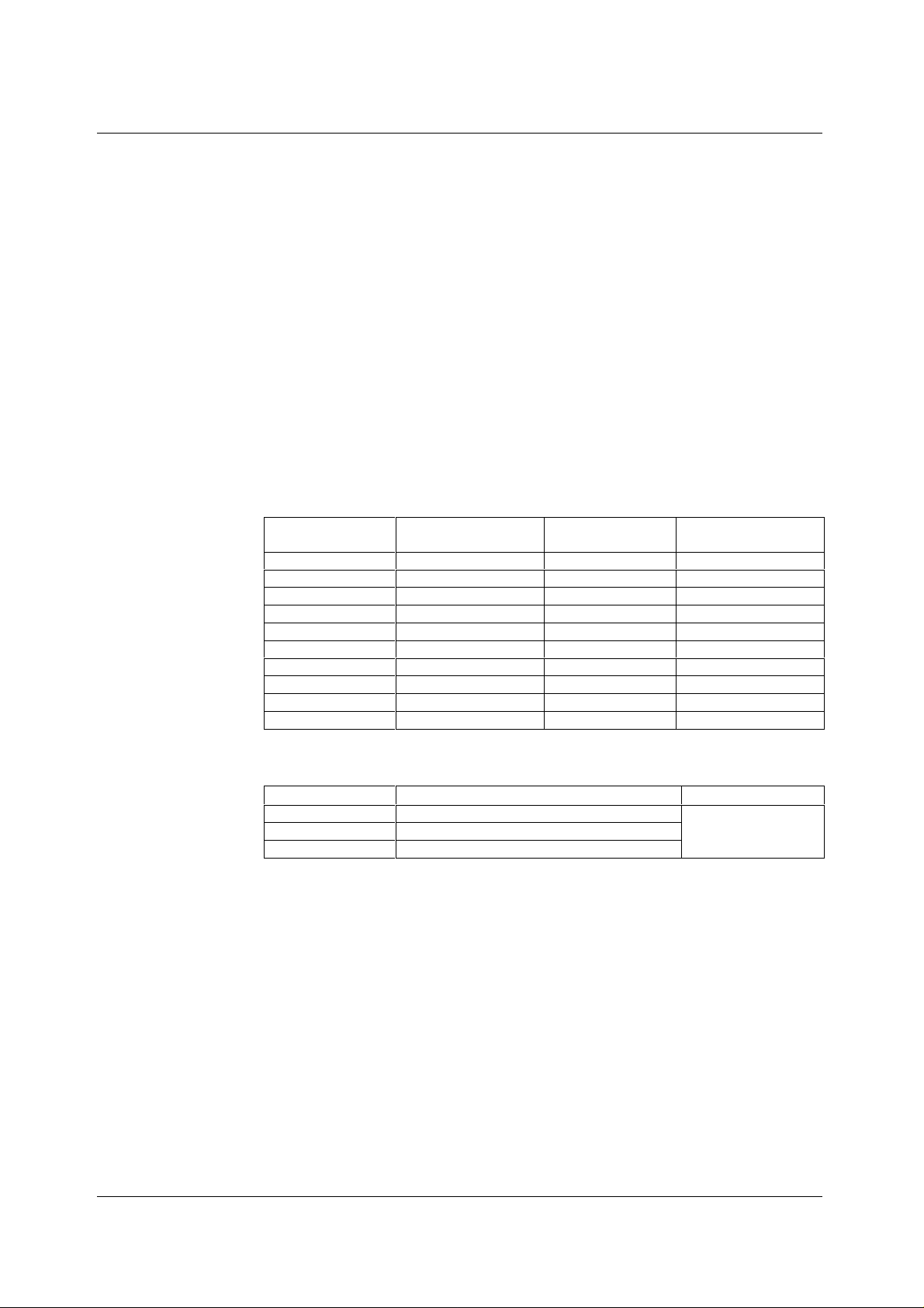
The following table shows which registers c ont rol which DAC rates, versus Mode and ID selected
CODEC ID FRONT DAC RATE REGISTER ADC RATE REG
00 and 01 2Ch
10 2Eh
11 2Ch (centre) and 30h (LFE)
Table 4 Variable Rate Register Location Versus ID
CONTROL VALUE
D15-D0
MODEM
SAMPLE RATE
12000 2EE0
13714.28 (96000/7) 3592
19200 4B00
24000 5DC0
CONTROL VALUE
D15-D0
32h
WOLFSON MICROELECTRONICS LTD PD Rev 3.4 January 2001
13
Page 14

WM9703 Production Data
GAIN CONTROL REGISTER LOCATION VERSUS ID
PGA CODEC ID CONTROL REG MUTE DE F AULT
Muted (bit-15)
AND with 38h, 7, 15
AND with 36h, 7, 15
Not-muted (bit-15)
Muted (15)
Muted (7 and 15)
Muted (7 and15)
DAC
Mixer
Volume
Table 5 Gain Control Register Location Versus ID
MASTER/SLAVE ID0/1 SUPPORT
WM9703 supports operation as either a master or a slave c odec. Configuration of the device as
either a master or as a s l ave, i s selected by tying the CID pins CID0 and CID1, pins 45 and 46 on the
package.
Fundamentally, a device identi fied as a m aster (ID = 00) produces BITCLK as an output, whereas a
slave (any other ID) must be provi ded with BITCLK as an i nput. Thi s has t he obvi ous im pl icat ion that
if the master devic e on an AC link is disabled, the slave devices cannot function.
The AC’97 Revision 2.1 specification defines that the CID pins have inverting sense, and are
provided with internal weak pull ups. Therefore, if no connections are made to the CI D0/1 pins, then
the pins pull hi and an ID = 00 is selected, i.e. master. External connects to ground will select other
IDs.
0x
10
11
0x
10
11
0x
10
11
18h
72h
02h
38h
36h
PIN46 CID1 PIN45 CID0 ID
NC NC 00 Master Output
NC Ground 01 Slave Input
Ground NC 10 Slave Input
Ground Ground 11 Slave Input
Table 6 ID Selection
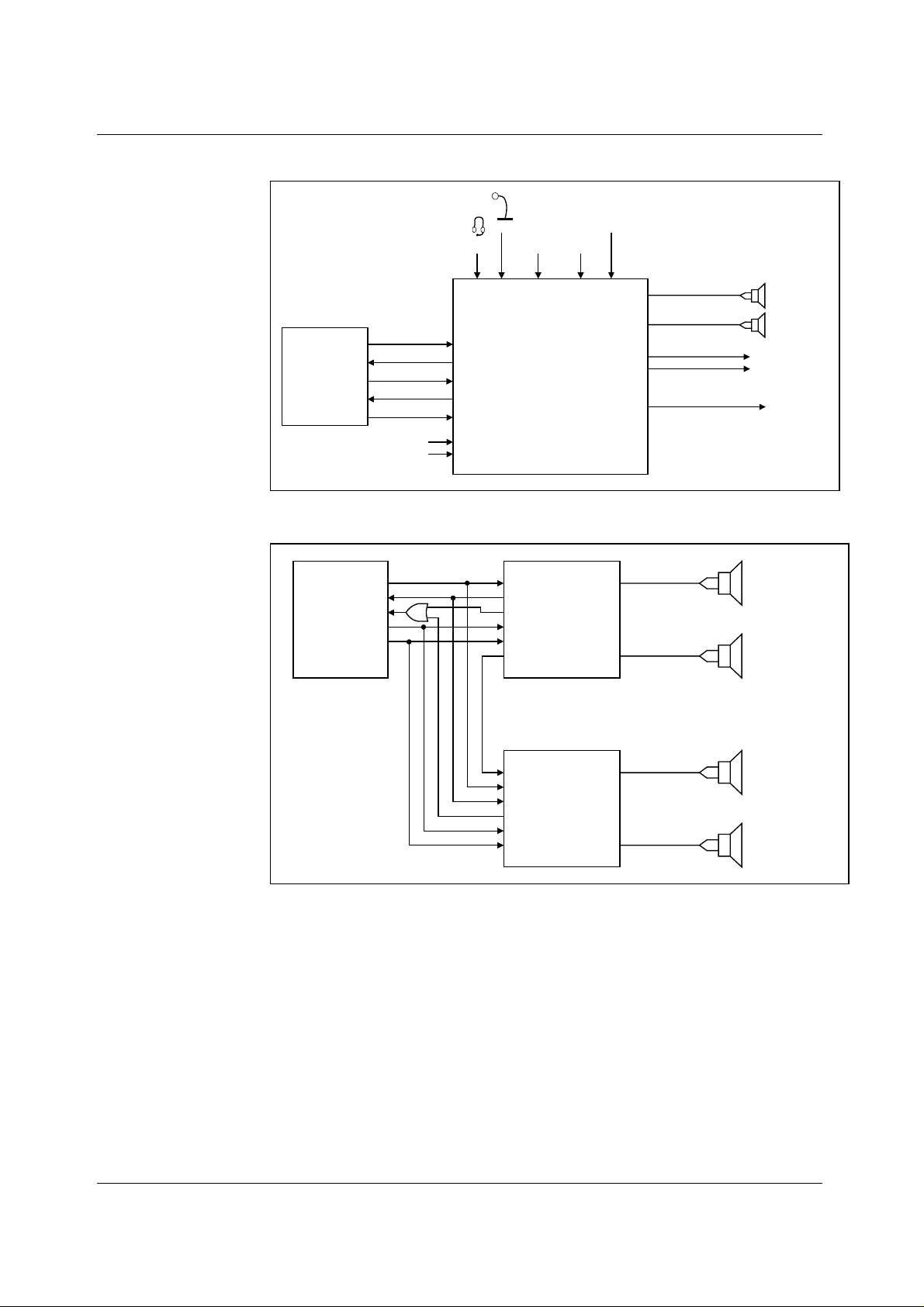
WM9703 supports the AMAP functi on whereby selection of an ID will automatically map t he data
from the interface ont o the PCM DACs. This allows a 6-channel audio system t o be built using 3
WM9703 devices, with one devic e c onfigured as a m as ter (I D 00) and t he other two as s laves (ID 10
and 11). (See figure 10). In this cas e, the main c hannel DACs will have mapped onto them the dat a
from the normal, s urround, and LFE and centre slots respectively, without any user select i on.
CODEC ID AC–LINK FRAME DATA
PCM left DAC uses
data from slot No.
00 3 4
01 3 4
10 7 8
11 6 9
The codec ID is available to t he controller via register 28h, bit s D15 and D14
Table 7 Default Slot to DAC Mappings Based on Codec ID
CODEC ID SLOTS MAPPED
TO DACS
00 or 01 3 and 4
10 7 and 8
11 6 and 9
Table 8 Slot to DAC and Mapping Based on Codec ID
SELECTED
USED FOR DACS
PCM right DAC uses
data from slot No.
MASTER OR
SLAVE
COMMENTS
Original definition (mas ter)
Original definition (docking)
Left/right surround channels
Centre/LFE channels
BITCLK
WOLFSON MICROELECTRONICS LTD PD Rev 3.4 January 2001
14
Page 15
Production Data WM9703
CONTROL INTERFACE
A digital interface has been provided t o control the WM9703 and transfer dat a to and from it. This
serial interface is compatible with the Intel AC’97.
The main control interfac e functions are:
• Control of analogue gain and signal paths through the mixer
• Bi-directional transfer of ADC and DAC words to and f rom AC’97 controller
• Selection of powerdown modes
AC-LINK DIGITAL SERIAL INTERFACE PROTOCOL
The WM9703 incorporates a 5-pin di gital serial interf ace that links it to the AC’97 cont roller. AC-link
is a bi-directional, fi xed rate, serial PCM digital stream. It handles multiple input and output audio
streams, as well as control register ac cesses em ploying a tim e division m ultiplexed (TDM) sc heme.
The AC-link architecture divides each audi o frame into 12 outgoing and 12 incom ing data streams,
each with 20-bit sample resolution. W ith a minimum requi red DAC and ADC resolution of 16-bits,
AC’97 may also be implem ented with 18 or 20-bit DA C/ADC resoluti on, given the headroom that the
AC-link architecture provi des. The WM9703 provides support for 18-bit operation.
SLOT
NUMBER
0123456789101112
SYNC
CMD
CMD
PCM
SDATA_OUT
SDATA_IN
CODEC ID
TAG
STATUS
TAG
SLOTREQ 3-12
ADR
ADDR
DATA
STATUS
DATA
LEFT
PCM
LEFT
PCM
RIGHT
PCM
RIGHT
TAG PHASE
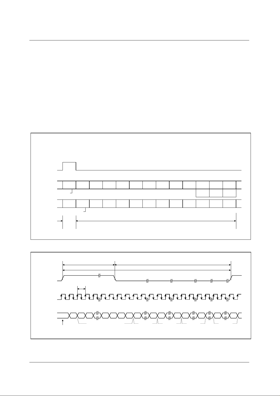
Figure 12 AC’97 Standard Bi-directional Audio Frame
TAG PHASE DATA PHASE
SYNC
12.288MHz
81.4nS
PCM
RSRVD
CENTRE
RSRVD RSRVD RSRVD RSRVD RSRVD RSRVD RSRVD RSRVD
PCM
L SURR
R SURR
PCM
PCM
LFE
RSRVD RSRVD
PCM R
PCM L
(n+1)
(n+1)
RSRVD
PCM C
(n+1)
DATA PHASE
20.8µS (48kHz)
BIT_CLK
SDATA_OUT
END OF PREVIOUS
AUDIO FRAME
SLOT(1) SLOT(2) SLOT(12)
FRAME
(’1’ = TIME SLOT CONTAINS
TIME SLOT ’VALID’ BITS
VALID PCM DATA)
’0’
(ID1) (ID0)
19 0 19 0 19 0 19 0
SLOT (1) SLOT (2) SLOT (3) SLOT (12)
VALID
Figure 13 AC-link Audio Output Frame
WOLFSON MICROELECTRONICS LTD PD Rev 3.4 January 2001
15
Page 16

WM9703 Production Data
The datastreams currentl y defined by the AC’97 specificat i on i nclude:
PCM playback - 2 output slots 2-channel composite PCM output stream
PCM record data - 2 input slots 2-channel composite PCM input stream
Control - 2 output slots Control register write port
Status - 2 input slots Control register read port
Optional modem line codec output -
1 output slot
Optional modem line codec input –
1 input slot
Optional dedicated microphone input -
1 input slot
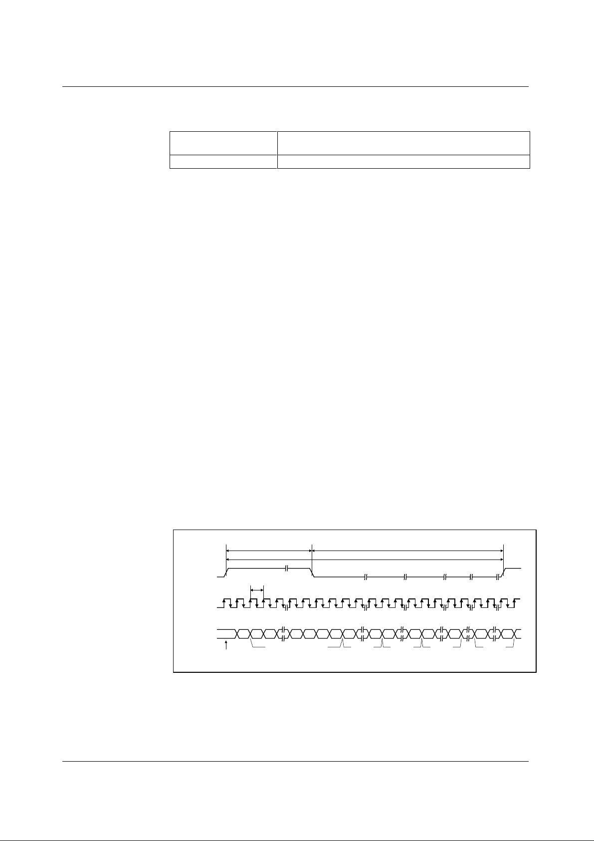
Synchronisation of all AC-link data transactions is s ignalled by the WM9703 controller. The W M9703
drives the serial bit clock onto AC-link, which the AC’97 controller then qualifies with a
synchronisation signal t o construct audio frames .
SYNC, fixed at 48kHz, is derived by di viding down the serial clock (BIT_CLK). BI T_CLK, fixed at
12.288MHz, provides the necessary clocking granularit y to support 12, 20-bit outgoing and incom ing
time slots. AC-link serial data is transit ioned on each ris ing edge of B IT_CLK . The rec eiver of A C-link
data, (WM9703 for outgoing dat a and AC’97 control ler for incom ing data), sampl es each s erial bit on
the falling edges of BIT_CLK.
The AC-link protocol provides for a special 16-bit time slot (slot 0) wherein each bit conveys a valid
tag for its corresponding t ime slot within the current audio f rame. A 1 in a given bit pos ition of slot 0
indicates that the correspondi ng tim e s lot within the c urrent audi o fram e has been ass igned t o a data
stream, and contains valid data. If a slot is t agged invalid, it is the respons ibility of t he source of the
data, (the WM9703 for the input stream, AC’97 controller for the output stream); to stuff all bit
positions with 0s during that slot’s active time.
SYNC remains high for a total duration of 16 BIT_CLKs at t he begi nni ng of each audio frame.
The portion of the audio frame where SYNC is high is defined as the Tag Phase. The rem ainder of
the audio frame where SYNC is low is defi ned as t he Data P hase. Addit ional ly, f or power savings , all
clock, sync, and data signals can be halted. This requires that the WM9703 be implem ented as a
static design to all ow its register contents to remain intact when entering a power savings mode.
Modem line codec DAC input s tream
Modem line codec ADC output stream
Dedicated microphone input stream in support
of stereo AEC and/or other voice applications.
AC-LINK AUDIO OUTPUT FRAME (SDATA_OUT)
The audio output frame data streams correspond to the mult iplexed bundles of all digit al output data
targeting the WM9703’s DAC inputs, and control registers. As briefly m entioned earlier, each audio
output frame supports up t o 12 20-bit outgoing data t ime sl ots. Slot 0 is a spec ial reserved time slot
containing 16-bits, which are used for AC-link protocol infrastructure.
OUTPUT TAG SLOT (16-BITS)
Bit (15) Frame Valid
Bit (14) Slot 1 Valid Command Address bit (Primary Codec only)
Bit (13) Slot 2 Valid Command Data bit (Primary Codec only)
Bit (12:3) Slot 3-12 Valid bits as def i ned by AC’97
Bit 2 Reserved (Set to 0)
Bit (1:0) 2-bit Codec I D f i el d (00 reserved for Pri mary; 01, 10, 11
New definitions for Secondary Codec Regi ster Access
Within sl ot 0 the first bit is a global bit (SDATA_OUT slot 0, bit 15) which flags the validit y for the
entire audio frame. If t he Valid Frame bit is a 1, t hi s indicates that the current audio frame contains at
least one time slot of valid dat a. The next 12-bit pos itions s ampl ed by the W M9703 indicat e which of
the corresponding 12 time s l ots contain valid data.
In this way data streams of differing sample rates can be transmitted across AC-link at its fixed
48kHz audio frame rate. Figure 13 illustrates the time slot based AC-link prot ocol.
indicate Secondary)
WOLFSON MICROELECTRONICS LTD PD Rev 3.4 January 2001
16
Page 17
Production Data WM9703
WM9703 SAMPLES
SYNC ASSERTION HERE
SYNC
WM9703 SAMPLES
FIRST SDATA_OUT
BIT OF FRAME HERE
BIT_CLK
VALID
SLOT (1) SLOT (2)
SDATA_OUT
END OF PREVIOUS AUDIO FRAME
FRAME
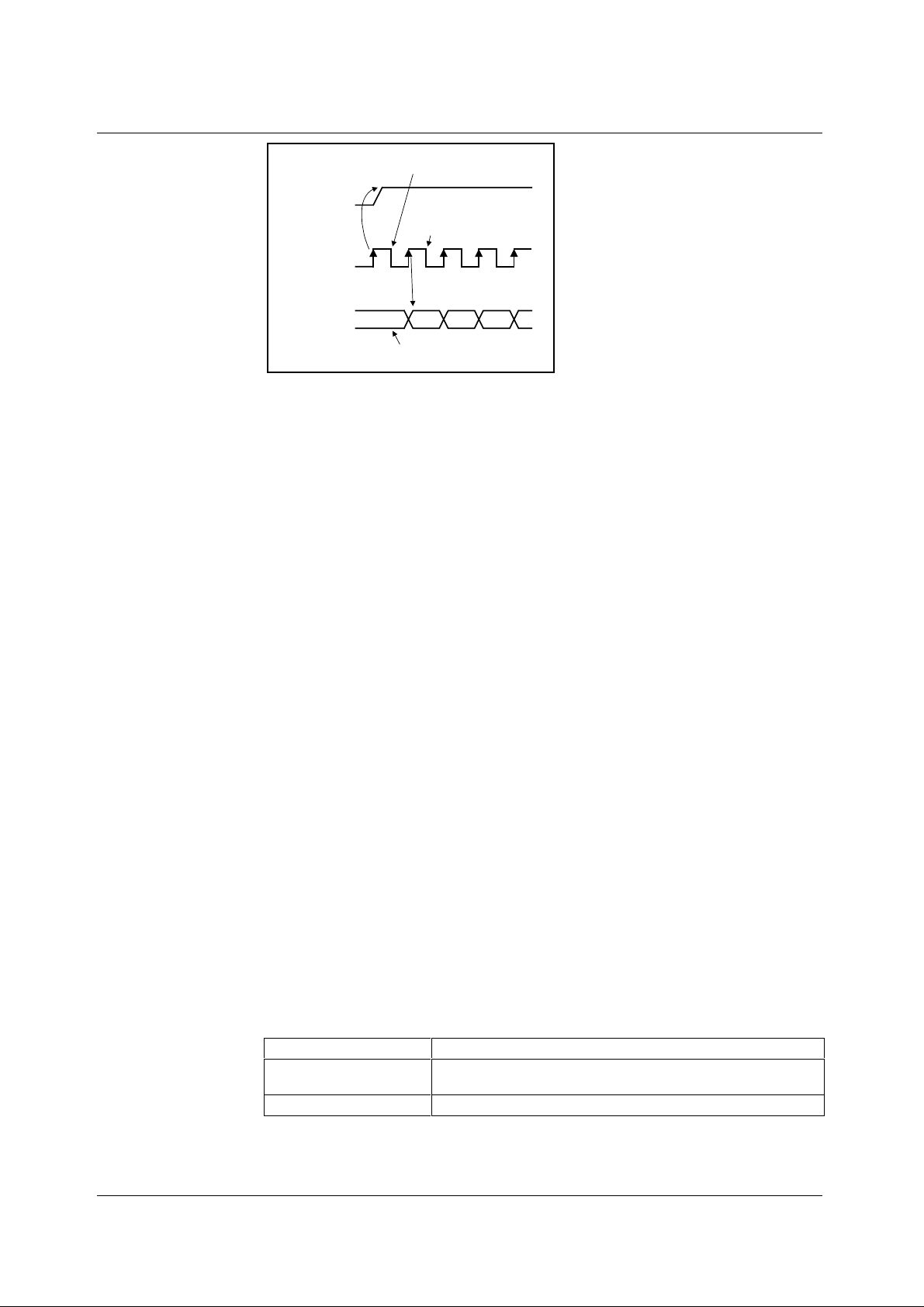
Figure 14 Start of an Audio Output Frame
A new audio output frame begins with a low to high trans iti on of SY NC as s hown in Figure 14. SY NC
is synchronous to the rising edge of BIT_CLK. On the imm ediat ely following falling edge of BI T_CLK,
the WM9703 samples the assertion of SYNC. This falling edge m arks the time when both sides of
AC-link are aware of the start of a new audio frame. On the next rising edge of BIT_CLK, AC’97
transitions SDATA_OUT i nto the first bit position of slot 0 (Vali d Frame bit). E ach new bit position is
presented to AC-link on a risi ng edge of BIT_CLK, and subsequently sampled by the WM9703 on the
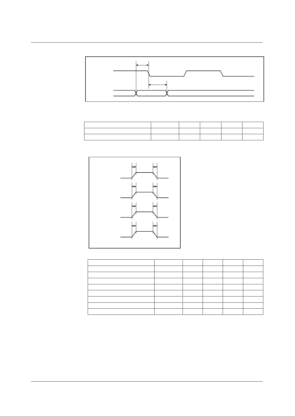
following falling edge of BIT_CLK. This sequence ensures that data transitions and subsequent
sample points for bot h i ncoming and outgoing data streams are time aligned.
Baseline AC’97 specified audio functionality MUST ALWAYS sample rate convert to and from a fixed
48ks/s on the AC’97 control ler.
This requirement is necessary to ensure that int eroperability between the AC’97 controller and the
WM9703, among other t hi ngs, can be guaranteed by definition for baseline specified AC’97 features.
SDATA_OUT’s composite stream is MSB justified (MSB first) with all non-valid slot bit positions
stuffed with 0s by the AC’97 controller.
In the event that there are less than 20 valid bi ts within an assigned and valid tim e slot, the AC’97
controller always stuffs al l trailing non-valid bit positions of the 20-bit slot with 0s.
As an example, consider an 8-bit s ample stream that is being played out to one of t he WM9703’s
DACs. The first 8 bit positi ons are presented to the DAC (MSB ju stified) followed by the next 12 bit
positions, which are stuffed with 0s by the AC’97 controller. This ensures that regardless of the
resolution of the implement ed DAC (16, 18 or 20-bit), no DC biasing will be introduced by the least
significant bits .
When mono audio s ample streams are output from the AC’97 cont roller, it is neces sary that BOTH
left and right sample stream time slots be filled with the same data.
SLOT 1: COMMAND ADDRESS PORT
The command port is used to control features, and monitor status for the WM9703 functions
including, but not limit ed to, mixer settings, and power management (refer to the register section).
The control interface archit ecture s upports up to 64, 16-bit read/write regis ters, address able on even
byte boundaries. Only the even registers (00h, 02h, etc.) are valid, odd register (01h, 03h, etc.)
accesses are disc ouraged (if supported they should default to t he preceding even byte boundary i.e. a read to 01h will return the 16-bit contents of 00h). The WM9703’s control register file is
nonetheless readable as well as writeable to provide more robust testability.
Audio output frame slot 1 communicates control register address, and read/write command
information to the WM9703.
COMMAND ADDRESS PORT BIT ASSIGNMENTS
Bit (19) Read/write command (1 = read, 0 = write)
Bit (18:12) Control register index (64 16-bit locations, addressed on even
Bit (11:0) Reserved (stuffed with 0s )
The first bit (MSB) sam pled by the WM9703 indicates whether the current control transact ion is a
read or write operation. The following 7 bit positions communicate the targeted control register
address. The trailing 12 bit positions within the slot are reserved and must be stuffed with 0s by the
AC’97 controller.
WOLFSON MICROELECTRONICS LTD PD Rev 3.4 January 2001
byte boundaries)
17
Page 18
WM9703 Production Data
SLOT 2: COMMAND DATA PORT
The command data port is used to deliver 16-bit control register write data in the event that the
current command port operation is a write cycle. (As indi cated by slot 1, bit 19).
Bit (19:4) Control register write data (stuffed with 0s if current operati on i s
a read)
Bit (3:0) Reserved (stuffed with 0s)
If the current comm and port operation is a read t hen the entire t ime slot must be stuff ed with 0s by
the AC’97 controller.
SLOT 3: PCM PLAYBACK LEFT CHANNEL
Audio output frame slot 3 is the com posite digital audio left playback stream . In a typical Games
Compatible PC this slot is com posed of st andard PCM (.wav) output sampl es digitally m ixed (on the
AC’97 controller or host processor) with music synthesis output samples. If a sample stream of
resolution less than 20-bits is transferred, the AC’97 controller must stuff all trailing non-valid bit
positions within this time slot with 0s.
SLOT 4: PCM PLAYBACK RIGHT CHANNEL
Audio output frame slot 4 is the composite digit al audio right playback stream . In a typical Games
Compatible PC this slot is com posed of st andard PCM (.wav) output sampl es digitally m ixed (on the
AC’97 controller or host processor) with music synthesis output samples.
If a sample stream of resolution less than 20-bit s is transferred, the AC’97 control ler must stuff all
trailing non-valid bit positi ons within this time s l ot with 0s.
SLOT 5: OPTIONAL MODEM LINE CODEC
Audio output frame slot 5 contains the MSB justified m odem DAC input data. This opt ional AC’97
feature is not supported in the WM9703, and if data is written to this loc ation it is ignored. This may
be determined by the AC’97 control l er i nt errogating the WM9703 Vendor ID registers.
SLOTS 6 TO 9: SURROUND SOUND DATA
Audio output frame slots 6 to 9 are used to send surround sound dat a. This dat a is m apped onto the
internal DACs depending on Codec ID, s ee Tabl e 8.
SLOTS 10 AND 11: LINE2 AND HANDSET DAC
These data slots are not support ed.
SLOT 12: GPIO CONTROL
These data slots are not support ed.
AC-LINK AUDIO INPUT FRAME (SDATA_IN)
TAG PHASE DATA PHASE
SYNC
BIT_CLK
SDATA_IN
END OF PREVIOUS
AUDIO FRAME
12.288MHz
81.4nS
CODEC
SLOT(1) SLOT(2) SLOT(12)
READY
(’1’ = TIME SLOT CONTAINS
’0’ ’0’ ’0’ 19 0 19 0 19 0 19 0
TIME SLOT ’VALID’ BITS
VALID PCM DATA)
SLOT (1) SLOT (2) SLOT (3) SLOT (12)
Figure 15 AC-link Audio Input Frame
The audio input frame data stream s correspond to the multiplexed bundles of all digital input data
targeting the AC’97 controller. As is t he case for audio output frame, eac h AC-link audio i nput frame
consists of 12, 20-bi t time slots.
Slot 0 is a special reserved time slot containing 16-bits, which are used for AC-link protocol
infrastructure.
WOLFSON MICROELECTRONICS LTD PD Rev 3.4 January 2001
20.8µS (48kHz)
18
Page 19
Production Data WM9703
Within slot 0 the firs t bit i s a global bit (SDATA_I N slot 0, bit 15) which fl ags whether the WM9703 is
in the Codec Ready state or not. If the Codec Ready bit is a 0, this i ndicates that t he W M9703 is not
ready for normal operation. This c ondition is normal following the desertion of power on reset for
example, while the WM9703’s voltage ref erences set tl e. When the AC-link Codec Ready indic ator bi t
is a 1, it indicates that the AC-link and the WM9703 control and status registers are in a fully
operational state. The AC’97 cont roller m ust f urther probe the Powerdown Control/St atus Regis ter to
determine exactly which subsec tions, if any, are ready.
Prior to any attempts at putting the W M9703 into operat ion the AC’97 c ontroller should poll the fi rst
bit in the audio input frame (S DATA_IN slot 0, bit 15) for an indicati on that the W M9703 has gone
Codec Ready.
Once the WM9703 is sam pled Codec Ready then the next 12 bit positions sam pled by the AC’97
controller indicate which of the corres ponding 12 time sl ots are assigned to i nput data stream s, and
that they contain valid data. Figure 15 illustrates the time slot based AC-link protocol.
There are several subsections withi n the WM9703 that can independently go busy/ready. It is the
responsibility of the WM9703 controller to probe more deeply into the WM9703 register file to
determine which the WM9703 subsections are actual l y ready.
WM9703 SAMPLES
SYNC ASSERTION HERE
SYNC
AC’97 CONTROLLER
SAMPLES FIRST SDATA_IN
BIT OF FRAME HERE
BIT_CLK
CODEC
SLOT (1) SLOT (2)
SDATA_IN
END OF PREVIOUS AUDIO FRAME
READY
Figure 16 Start of an Audio Input Frame
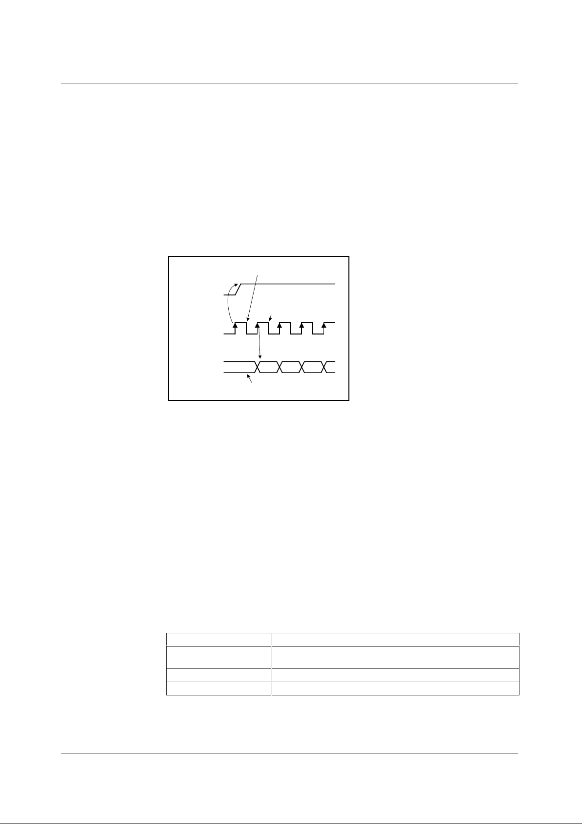
A new audio input frame begins with a low to high transi tion of SYNC as shown in Figure 16. SYNC
is synchronous to the rising edge of BIT_CLK. On the imm ediat ely following falling edge of BI T_CLK,
AC’97 samples the assertion of SYNC. This falling edge m arks the ti me when both sides of AC-link
are aware of the start of a new audio frame. On the next rising of BIT_CLK, AC’97 transitions
SDATA_IN into the first bit posi tion of s lot 0 (“Codec Ready” bit). Each new bit posi tion is pres ented
to AC-link on a rising edge of BI T_CLK, and subsequently sampl ed by the AC’97 Controller on the
following falling edge of BIT_CLK. This sequence ensures that data transitions and subsequent
sample points for bot h i ncoming and outgoing data streams are time aligned.
SDATA_IN’s composite stream is MSB justified (MSB first) with all non-valid bit positions (for
assigned and/or unassigned time slots) stuffed with 0s by the WM9703. SDATA_IN should be
sampled on the falling edges of BIT_CLK.
SLOT 1: STATUS ADDRESS PORT
The status port is used t o monitor status for the WM9703 functions i ncluding, but not limit ed to, mixer
settings, and power management.
Audio input frame slot 1 echoes the control register index, for his torical reference, for the data to
be returned in slot 2. (Ass um ing that sl ots 1 and 2 had been t agged valid by the WM9703 during slot
0).
STATUS ADDRESS PORT BIT ASSIGNMENTS:
Bit (19) RESERVED (stuffed with 0s)
Bit (18:12) Control register index (echo of register index for which data i s
Bit (11:2) Variable sample rat e S LOTRE Q bi ts.
Bit (1:0) RESERVED (stuffed with 0s)
The first bit (MSB) generated by the WM9703 is always stuffed with an 0. The following 7 bit
positions comm unicat e the ass ociated c ontrol regis ter address. The next 10 bit s s upport t he AC ’97
Rev 2.1 variable sample rate signalling protocol, and the trailing 2 bit posit ions are stuf fed with 0s by
AC’97.
WOLFSON MICROELECTRONICS LTD PD Rev 3.4 January 2001
being returned)
19
Page 20

WM9703 Production Data
SLOT 2: STATUS DATA PORT
The status data port delivers 16-bi t control register read data.
Bit (19:4) Control register read data (s t uffed with 0s if tagged invalid by
Bit (3:0) RESERVED (stuffed with 0s)
If slot 2 is tagged invalid by the WM9703, then the entire slot will be stuffed with 0s by the WM9703.
WM9701)
SLOT 3: PCM RECORD LEFT CHANNEL
Audio input frame slot 3 i s the left channel output of the WM9703’s input Mux, post-ADC.
The WM9703 sends out its ADC output dat a (MSB f irst ), and s tuff s any t railing non-valid bit posit ions
with 0s to fill out its 20-bit time slot.
SLOT 4: PCM RECORD RIGHT CHANNEL
Audio input frame slot 4 i s the right channel output of the WM9703’s input Mux, post-ADC.
The WM9703’s ADCs can be i mplemented to support 16, 18, or 20-bit resolution.
The WM9703 ships out its A DC output data (MSB first), and stuff s any trailing non-valid bit pos itions
with 0s to fill out its 20-bit time slot.
SLOT 5: OPTIONAL MODEM LINE CODEC
Audio input frame slot 5 contains MSB justi fied m odem ADC out put data. Thi s optional feature is not
supported by WM9703. This may be determined by the AC’97 cont roller interrogating the W M9703
Vendor ID register.
SLOT 6: OPTIONAL DEDICATED MICROPHONE RECORD DATA
Audio input frame slot 6 is an optional (post -ADC) third PCM system, input channel available for
dedicated use by a desktop microphone. This optional AC’97 feature is not supported by the
WM9703. This may be determined by the AC’97 controller interrogating the W M9703 Vendor ID
register.
SLOTS 7 TO 12: RESERVED
Audio input frame slots 7 to 12 are reserved for fut ure use and are always stuffed with 0s by the
WM9703.
AC-LINK LOW POWER MODE
The AC-link signals can be placed in a low power mode. W hen the WM9703’s P owerdown Register
26h, is programmed to the appropriate value, both BIT_CLK and SDATA _IN will be brought to, and
held at a logic low voltage level.
BIT_CLK and SDATA_IN are trans itioned low immediately following the decode of t he write to the
Powerdown Register 26h with PR4. When the AC’97 c ontroller dri ver is at the poi nt where it is ready
to program the AC-link into its low power mode, s lots 1 and 2 are assumed to be the only valid
stream in the audio output f rame. At this point in time it is ass umed that all sources of audio input
have also been neutralised.
The AC’97 controller should also drive S YNC and SDATA _OUT low after programm ing the WM9703
to this low power, halted mode.
Once the WM9703 has been instruc ted t o halt B IT_CLK , a s peci al wake up protoc ol m ust be used t o
bring the AC-link to the active mode since normal audio output and input frames can not be
communicated i n the absence of BIT_CLK.
WAKING UP THE AC-LINK
There are 2 methods for bringing the AC-link out of a low power, halted mode. Regardless of the
method, it is the AC’97 controller that perform s the wake up task.
AC-link protocol provides f or a Col d WM9703 Reset, and a Warm WM9703 Res et.
The current powerdown state would ultimately dict ate which form of WM9703 reset is appropriate.
Unless a cold or register reset (a write to the reset register) is performed, wherein the WM9703
registers are initialised to their default values, registers are required to keep state during all
powerdown modes.
WOLFSON MICROELECTRONICS LTD PD Rev 3.4 January 2001
20
Page 21

Production Data WM9703
Once powered down, re-activation of the AC-link via re-assertion of t he SYNC signal m ust not oc cur
for a minimum of 4 audio frame times f ollowing the frame in which the powerdown was triggered.
When AC-link powers up it i ndi cates readiness via the Codec Ready bi t (input slot 0, bit 15).
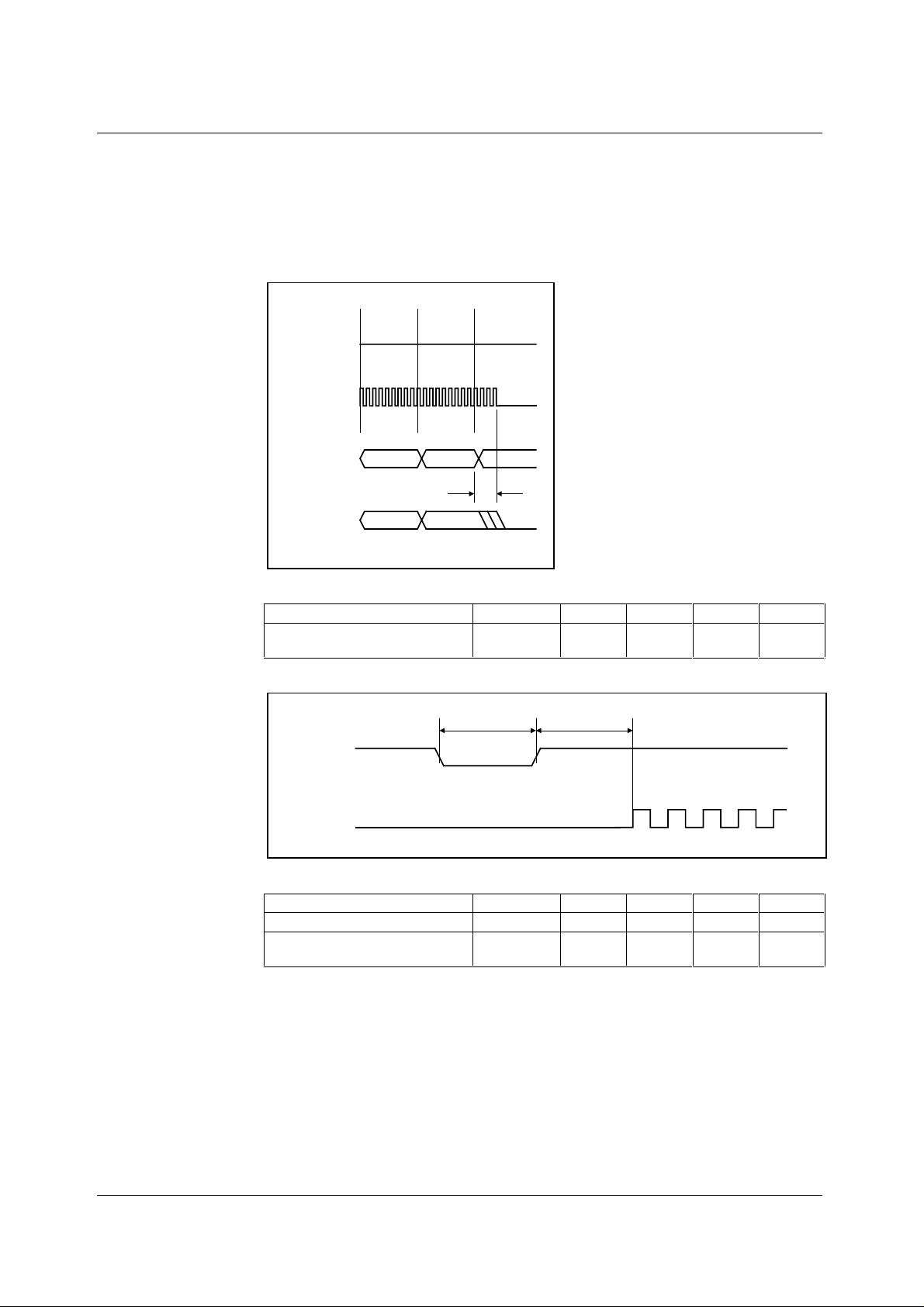
COLD WM9703 RESET
A cold reset is achieved by asserting RESETB for the minimum specified time. By driving RESETB
low, BIT_CLK, and SDATA_OUT will be activated, or re-activated as the case may be, and all the
WM9703 control registers will be initialised t o t heir default power on reset values.
RESETB is an asynchronous WM9703 input.
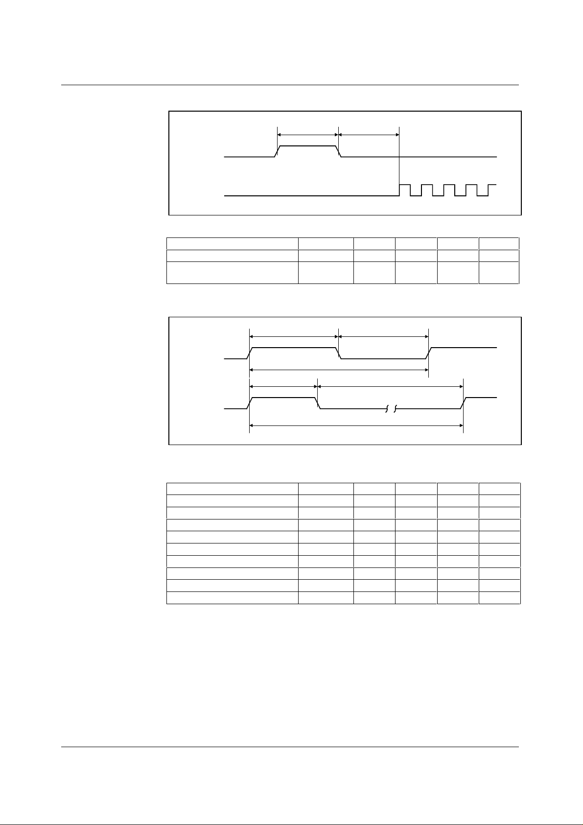
WARM WM9703 RESET
A warm WM9703 reset will re-activate the AC-link without altering the current WM9703 register
values. A warm reset is signalled by driving S YNC high for a minimum of 1µS in the absence of
BIT_CLK.
Within norm al audio frames SYNC is a synchronous input. I n the absence of BIT_CLK, SYNC is
treated as an asynchronous input used in the generation of a warm reset to the WM9703. The
WM9703 will not respond with the activation of BIT_CLK until SYNC has been sampled low again by
the WM9703. This will preclude the false det ection of a new audio frame.
SERIAL INTERFACE REGISTER MAP DESCRIPTION
(See Table 21)
The serial interface bits perform control functions described as follows: The register map is fully
specified by the AC’97 specification, and this description is simply repeated below, with optional
unsupported features omit ted.
RESET REGISTER (INDEX 00h)
Writing any value to t hi s register performs a register reset, which causes al l registers to revert to their
default values. Reading this regi ster returns the ID code of the part, indicati on of modem support (not
supported by the WM9703) and a code for the type of 3D stereo enhancement .
The ID decodes the capabilities of the WM9703 based on the following:
BIT FUNCTION VALUE ON
ID0
ID1
ID2
ID3
ID4
ID5
ID6
ID7
ID8
ID9
SE4...SE0
Table 9 Reset Register Function
Note that the WM9703 defaults to indicate 18-bit com patibility. However, a control bit m ay be set in
the vendor-specific registers that changes bits ID6 and ID8 to be 0, indicating a 16-bit devi ce. It is
unlikely that this function will be required, however, as the MSB justification of the ADC and DAC
data means that a nominally 18-bit device should be fully compatible with controllers that only
provide 16-bit support. Most PC type applications will only require 16-bit operation.
Dedicated Mic PCM in channel
Modem line codec support
Bass and treble control
Simulated stereo (mono to stereo)
Headphone out support
Loudness (bass boost) support
18-bit DAC resolution
20-bit DAC resolution
18-bit ADC resolution
20-bit ADC resolution
Wolfson Microel ectronics 3D enhancement
WM9703
0
0
0
0
1
0
1
0
1
0
11000
PLAY MASTER VOLUME REGISTERS (INDEX 02h, 04h AND 06h)
These registers manage the output signal volumes . Register 02h control s the stereo m aster volume
(both right and left channels), Regis ter 04h cont rols the opt ional stereo headphone out , and Regis ter
06h controls the mono volum e output. Each st ep corresponds to 1.5dB. The MSB of the register is
the mute bit. When this bit is set to 1 the level for that c hannel i s set at -
ML5 to ML0 is for left channel level, MR5 to MR0 is for the right channel and MM5 to MM0 is for the
mono out channel.
WOLFSON MICROELECTRONICS LTD PD Rev 3.4 January 2001
∞dB.
21
Page 22

WM9703 Production Data
Support for the MSB of the volum e level is not provided by the W M9703. If the MSB is written to,
then the WM9703 detects when that bit is set and sets al l 4 LSBs to 1s. Example: If the dri ver writes
a 1xxxxx th e WM9703 interpret s that as x11111. It will also respond when read with x11111 rather
than 1xxxxx, the valu e written to it. The driver can us e this fea ture to det ect if support f or the 6t h bit is
there or not.
The default value of both the mono and the stereo registers is 8000h (1000 0000 0000 0000), which
corresponds to 0dB gain with mut e on.
MUTE MX4...MX0 FUNCTION
0 0 0000
0 0 0001
0 1 1111
1 x xxxx
Table 10 Volume Register Function
MASTER TONE CONTROL REGISTERS (INDEX 08h)
Optional register for support of tone controls (bass and treble). The W M9703 does not s upport bass
and treble and writing to this register will have no effect. Reading will result in all don’t care values.
PC BEEP REGISTER (INDEX 0Ah)
This controls the level for the PC-beep input. Each step corresponds to approximately 3dB of
attenuation. The MSB of the register is the mute bit. When this bit is set to 1 the level for that
channel is set at -
WM9703 defaults to the PC-beep path being muted, so an external speaker should be provided
within the PC to alert the user to power on self -test problems.
∞dB.
0dB attenuation
1.5dB attenuation
46.5dB attenuation
∞dB attenuation
MUTE PV3...PV0 FUNCTION
0 0000
0 1111
1 xxxx
Table 11 PC-beep Register Function
0dB attenuation
45dB attenuation
∞dB attenuation
ANALOGUE MIXER INPUT GAIN REGISTERS (INDEX 0Ch - 18h)
This controls the gain/attenuation for each of the analogue inputs. Each step corresponds to
approximately 1.5dB. The MSB of the regi ster is the mut e bit. When t his bit is set t o 1 the level for
that channel is set at -
∞dB.
REGISTER 0Eh (MIC VOLUME REGISTER)
This has an extra bit that is for a 20dB boost. When bit 6 is set to 1 the 20dB boos t is on. The default
value is 8008, which corresponds to 0dB gai n with mute on.
The default value for the mono regis ters is 8008h, which corres ponds to 0dB gai n with mute on. The
default value for stereo registers is 8808h, which corresponds to 0dB gain with mute on.
MUTE GX4...GX0 FUNCTION
0 00000
0 01000
0 11111
1 XXXXX
Table 12 Mixer Gain Control Register Function
+12dB gain
0dB gain
-34.5dB gain
∞dB gain
-
WOLFSON MICROELECTRONICS LTD PD Rev 3.4 January 2001
22
Page 23

Production Data WM9703
RECORD SELECT CONTROL REGISTER (INDEX 1Ah)
Used to select the record source independently for right and left (see Table 13). The default value is
0000h, which corresponds to Mic in.
SR2 TO SR0 RIGHT RECORD SOURCE SL2 TO SL0 LEFT RECORD SOURCE
0
1
2
3
4
5
6
7
Table 13 Record Select Register Function
Mic
CD in (R)
Video in (R)
Aux in (R)
Line in (R)
Stereo mix (R)
Mono mix
Phone
0
1
2
3
4
5
6
7
Mic
CD in (L)
Video in (L)
Aux in (L)
Line in (L)
Stereo mix (L)
Mono mix
Phone
RECORD GAIN REGISTERS (INDEX 1Ch AND 1Eh)
1Ch is for the stereo input and 1Eh i s for the optional special purpos e correlated audio Mic channel.
Each step corresponds to 1.5dB. 22.5dB corresponds to 0F0Fh and 000Fh res pectively. The MSB of
the register is the m ute bit. When thi s bit is set to 1, t he l evel for that channel(s) is set at -∞dB.
The default value is 8000h, which corresponds to 0dB gain with mute on.
MUTE GX3...GX0 FUNCTION
0
0
1
Table 14 Record Gain Register Function
1111 +22.5dB gain
0000 0dB gain
xxxxx -
∞dB gain
GENERAL PURPOSE REGISTER (INDEX 20h)
This register is used to control several misc el l aneous functions of the WM9703.
Below is a summary of each bit and its funct ion. Only the 3D, MIX, MS and LPBK bits are support ed
by the WM9703. The MS bit controls t he Mic selector. The LPBK bit enables loopback of the ADC
output to the DAC input without involving the AC-link, allowing for full system performance
measurements. The f unction default value is 8000h which is al l of f.
BIT FUNCTION WM9703
SUPPORT
POP
ST
3D
LD
LLBK
RLBK
MIX
MS
LPBK
Table 15 General Purpose Register Function
PCM out path and mute, 0 = pre-3D, 1 = post -3D Yes, but fixed at 1
Simulated stereo enhancement, on/off 1 = on No
3D stereo enhancement on/off, 1 = on Yes
Loudness (bass boost) on/off, 1 = on No
Local loop back - for modem, line codec No
Remote loop back - for modem, line codec No
Mono output select 0 = Mix, 1 = Mic Y es
Mic select 0 = Mic1, 1 = Mic2 Yes
ADC/DAC/ loopback mode Yes
3D CONTROL REGISTER (INDEX 22h)
This register is used to control the centre and/or depth of t he 3D stereo enhancement func tion built
into of the AC’97 component. Only the depth bits, DP0 to 3 have ef fect in the WM9703.
DP3…DP0 DEPTH
00%
1
8 Typical value
-
15 100%
WOLFSON MICROELECTRONICS LTD PD Rev 3.4 January 2001
23
Page 24

WM9703 Production Data
RESERVED REGISTER (INDEX 24h)
This register was originally specified to control what sample rate AC’97 is sending or receiving
samples for the opti onal modem in and out. Not supported by the WM9703.
POWERDOWN CONTROL/STATUS REGISTER (INDEX 26h)
This read/write register is used to program powerdown states and m onit or subs yst em readines s. The
lower half of this register is read only s tatus, a 1 indicating that the s ubsection is ready. Ready is
defined as the subsecti on able to perform in its nominal state. When this register is written the bit
values that come in on AC-link will have no effect on read only bits 0 to7.
When the AC-link Codec Ready indi cat or bit (SDATA _IN s lot 0, bit 15) is a 1 it i ndic ates t hat the A Clink and the WM9703 control and status registers are i n a f ul l y operat i onal state. The AC’97 controller
must further probe this Powerdown Control/Status Regis ter to determ ine exactly which subsections ,
if any, are ready.
READ BIT FUNCTION
REF
ANL
DAC
ADC
Table 16 Powerdown Status Register Function
The powerdown modes are as follows. The first three bits are to be used individually rather t han in
combination with each other. The last bit P R3 can be used in c ombinat ion with PR2 or by its elf. P R0
and PR1 control the PCM ADCs and DACs onl y. PR6 is not supported by the WM9703.
WRITE BIT FUNCTION
PR0 PCM in ADCs and input Mux powerdown
PR1 PCM out DACs powerdown
PR2 Analogue mixer powerdown
PR3 Analogue mixer powerdown (VREF off)
PR4 Digital interface (AC-l i nk) powerdown
PR5 Internal clock dis able
PR6 HP amp powerdown – not supported
EAPD External amplifier powerdown
Table 17 Powerdown Control Register Function
VREFs up to nominal level
Analogue mixers, etc ready
DAC section ready to acc ept data
ADC section ready to transmit data
(VREF still on)
(external clock off)
NORMAL
PR0 = 1
PR0 = 0 AND
ADC = 1
ADCs OFF
READY = 1
PR1 = 1 PR2 = 1 PR4 = 1
DAC = 1
DACs OFF
PR1
PR2 = 0 AND
ANL = 1
DEFAULT
PR0
PR1 = 0 AND
ANALOGUE
OFF PR2 OR
PR3
DIGITAL I/F
OFF PR4
WARM
RESET
COLD RESET
SHUT OFF
CODA LINK
Figure 17 An Example of the WM9703 Powerdown/Powerup Flow
WOLFSON MICROELECTRONICS LTD PD Rev 3.4 January 2001
24
Page 25

Production Data WM9703
Figure 17 illustrates one example of a procedure to do a com plet e powerdown of the WM9703. From
normal operation sequential writes to the Powerdown Register are performed to powerdown the
WM9703 a piece at a time. After everything has been shut off (PR0 to PR3 set), a final write (of PR4)
can be executed to shut down the WM9703’s di gi tal interface (AC-link).
The part will remain in sleep mode with all its registers holding their static values. To wake up the
WM9703, the AC’97 controller will send a pulse on the sync line issuing a warm reset. This will
restart the W M9703’s digital interf ace (resetti ng PR4 to 0). The W M9703 can also be woken up with
a cold reset. A cold reset will cause a loss of values of the registers, as a cold reset will set them to
their default states. When a section is powered back on, the Powerdown Control/Status Register
index 26h should be read to verify that the section is ready (i.e. stable) before attempting any
operation that requires it.
Alternatively if RESETB is held low, all PR bits are held set so the device is held powered off until
RESETB is taken high again.
ADCs OFF
PR0
PR1 = 1
PR1 = 0 AND
DAC = 1
DACs OFF
PR2 = 1 PR4 = 1
PR1
PR2 = 0 AND
ANL = 1
ANALOGUE
OFF PR2
OR PR3
DIGITAL I/F
OFF PR4
WARM RESET
SHUT OFF
CODA LINK
Figure 18 The WM9703 Powerdown/Flow with Analogue Still Alive
Figure 18 illustrates a state when all the mixers should work with the s tatic volume sett ings that are
contained in their associated registers. This is used when the user is playing a CD (or external
LINEIN source) through WM9703 to t he speakers but has most of the system in low power mode.
The procedure for this follows the previous except that the analogue mixer is never shut down.
POWERDOWN CONTROL/STATUS REGISTER (INDEX 26h)
Note that in order to go into ultim ate low power mode, PR5 is required to be set which t urns off t he
oscillator circuit. Asserting SYNC res ets the PR5 bit and re-starts the oscillator in the sam e was as
the AC link is restart ed.
Also when RESETB pin is asserted low, all PR bits are over-ridden and the entire device is powered
off to ultra low power state for as long as RESETB = low. On releas ing RESETB, the device is res et
(all active) and powered up.
REVISION 2.1 REGISTERS (INDEX 28h T0 58h)
These registers are specified as to use in Revision 2.1 of the AC’97 specification and have the
following functions on the WM9703:
REGISTER 28h – EXTENDED AUDIO ID
The Extended Audio ID register is a read only register that identifies which extended audio feat ures
are supported (in addition to the original AC’97 features identified by reading the reset regist er at
index 00h). A non zero value indicates the feat ure i s supported.
WOLFSON MICROELECTRONICS LTD PD Rev 3.4 January 2001
25
Page 26

WM9703 Production Data
DATA BIT FUNCTION ANY MODE
VRA
DRA
VRM
CDAC
SDAC
LDAC
AMAP
ID1
ID0
Table 18 Extended Audio Capability Register
REGISTER 2Ah – EXTENDED AUDIO STATUS AND CONTROL REGISTER
The Extended Audio Status and Control Regis ter is a read/write register that provides stat us and
control of the extended audio features.
DATA BIT FUNCTION READ/WRITE WM9703 SUPPORT
VRA
DRA
VRM
CDAC
SDAC
LDAC
MADC
PRI
PRJ
PRK
PRL
Table 19 Extended Audio Status and Control Register
Variable rate audio support
Double rate audio support
Variable rate Mic ADC support
Centre DAC support
Surround DAC support
LFE DAC support
Slot to front DAC m appi ng support
Codec configuration – pin 45 value
Codec configuration – pin 46 value
Enables variable rate audio mode
Enable double rate audio mode
Enables variable rate Mic ADC
Indicates centre DAC ready
Indicates surround DAC ready
Indicates LFE DAC ready
Indicates Mic ADC ready
Set to turn off centre DAC
Set to turn off surround DA Cs
Set to turn off LFE DACs
Set to turn off Mic ADC
1
0
0
0
0
0
1
Inverse of level at pin 45
Inverse of level at pin 46
Read/write Yes
Read/write No
Read/write No
Read Yes
Read Yes
Read Yes
Read No
Read/write Enable only
Read/write Enable only
Read/write Enable only
Read/write No
REGISTER 2Ch TO 32h – AUDIO SAMPLE RATE CONTROL REGISTERS
These registers are read/write registers that are written to, to selec t alternative sampl e rates for the
audio PCM converters. Default is the 48ks/s rate. Not e that only Revision 2.1 recommended rates
are supported by the WM9703, selection of any other uns upported rat es will caus e the rate t o default
to the nearest supported rate, and the supported rate value to be latched and s o read back.
Register 2Ch is the front DAC rate register, but is als o used for centre channel data rate.
REGISTERS 36h AND 38h – 6 CHANNEL VOLUME CONTROL
These read/write registers control the output volume of the optional four PCM channels. (not
supported by the WM9703)
VENDOR RESERVED REGISTERS (INDEX 5Ah AND 7Ah)
These registers are vendor specific. Do not write t o thes e regis ters unless the V endor ID regis ter has
been checked first to ensure that the driver knows the source of the AC ‘97 component.
VENDOR SPECIFIC GAIN CONTROL REGISTERS – (INDEX 70h TO 74h)
Not used in the WM9703.
VENDOR ID REGISTERS (INDEX 7Ch TO 7Eh)
This register is for spec ific vendor ident ificati on if so desired. The ID method is Micros oft’s P lug and
Play Vendor ID code. The first character of that I D is F7 to F0, the s econd charact er S7 to S 0, and
the third T7 to T0. These three charac ters are ASCII encoded. The REVIS ION7 to RE VISION0 field
is for the Vendor Revision number. In the WM9703 the vendor ID is set to WML3.
Wolfson is a registered Microsoft Plug and Play vendor.
WOLFSON MICROELECTRONICS LTD PD Rev 3.4 January 2001
26
Page 27

Production Data WM9703
SERIAL INTERFACE REGISTER MAP
The following table shows the function and address of the various control bi ts that are loaded through
the serial interface during write operat i ons.
RegName D15D14D13D12D11D10D9D8D7D6D5D4D3D2D1 D0 efault
00h Reset X SE4 SE3 SE2 SE1 SE0 ID9 ID8 ID7 ID6 ID5 ID4 ID3 ID2 ID1 ID0 6150h
02h Master volume Mute X X ML4 ML3 ML2 ML1 ML0 X X X MR4 MR3 MR2 MR1 MR0 8000h
04h LNLVL volume Mute X X ML4 ML3 ML2 ML1 ML0 X X X MR4 MR3 MR2 MR1 MR0 8000h
06h Master volume
mono
0Ah PCBEEP volume Mute X XXXXXXXXXPV3PV2PV2PV0X8000h
0Ch Phone volume Mute X XXXXXXXXXGN4GN3GN2GN1GN08008h
0EhMic volume MuteXXXXXXXX20dB X GN4 GN3 GN2 GN1 GN0 8008h
10h Line in volume Mute X X GL4 GL3 GL2 GL1 GL0 X X X GR4 GR3 GR2 GR1 GR0 8808h
12h CD volume Mute X X GL4 GL3 GL2 GL1 GL0 X X X GR4 GR3 GR2 GR1 GR0 8808h
14h Video volume Mute X X GL4 GL3 GL2 GL1 GL0 X X X GR4 GR3 GR2 GR1 GR0 8808h
16h Aux volume Mute X X GL4 GL3 GL2 GL1 GL0 X X X GR4 GR3 GR2 GR1 GR0 8808h
18h PCM out volume Mute X X GL4 GL3 GL2 GL1 GL0 X X X GR4 GR3 GR2 GR1 GR0 8808h
1AhRec select XXXXXSL2SL1SL0XXXXXSR2SR1SR00000h
1ChRec gain MuteXXXGL3GL2GL1GL0XXXXGR3GR2GR1GR08000h
20h General purpose POP ST 3D lD X X MIX MS LPBK XXXXXX X0000h
22h3D control XXXXXXXXXXXXDP3DP2DP1DP00000h
24hReserved xxxxxxxxxxxxxxx x0000h
26h Power/down control
status
28h Ext’d audio ID ID1 ID0 XXXXAmapLdac Sdac Cdac X X VRM X DRA VRA 0201h
2Ah Ext’d audio stat/ctrl X PRL PRK PRJ PRI X Madc Ldac Sdac Cdac X X VRM X DRA VRA 0000h
2Ch Front DAC rate SR15 SR14 SR13 SR12 SR11 SR10 SR9 SR8 SR7 SR6 SR5 SR4 SR3 SR2 SR1 SR0 BB80h
32h Audio ADC rate SR15 SR14 SR13 SR12 SR11 SR10 SR9 SR8 SR7 SR6 SR5 SR4 SR3 SR2 SR1 SR0 BB80h
72h Front mixer volume Mute X X GL4 GL3 GL2 GL1 GL0 X X X GR4 GR3 GR2 GR1 GR0 0808h
74h Surround sound X X XXXXXXXXXXXXX X0000h
7Ah Vendor reserved X X XXXXXXXXXXXXX X0000h
7Ch Vendor ID1 F7 F6 F5 F4 F3 F2 F1 F0 S7 S6 S5 S4 S3 S2 S1 S0 574Dh
7Eh Vendor ID2 T7 T6 T5 T4 T3 T2 T1 T0 Rev7 Rev6 Rev5 Rev4 Rev3 Rev2 Rev1 Rev0 4C03h
Table 21 Serial Interface Register Map Description
MuteXXXXXXXXXXMM4MM3MM2MM1MM08000h
APDXPR5PR4PR3PR2PR1PR0XXXXREFANLDACADC000Fh
WOLFSON MICROELECTRONICS LTD PD Rev 3.4 January 2001
27
Page 28
WM9703 Production Data RECOMMENDED EXTERNAL COMPONENTS
MASTER/
SLAVE
CONTROL
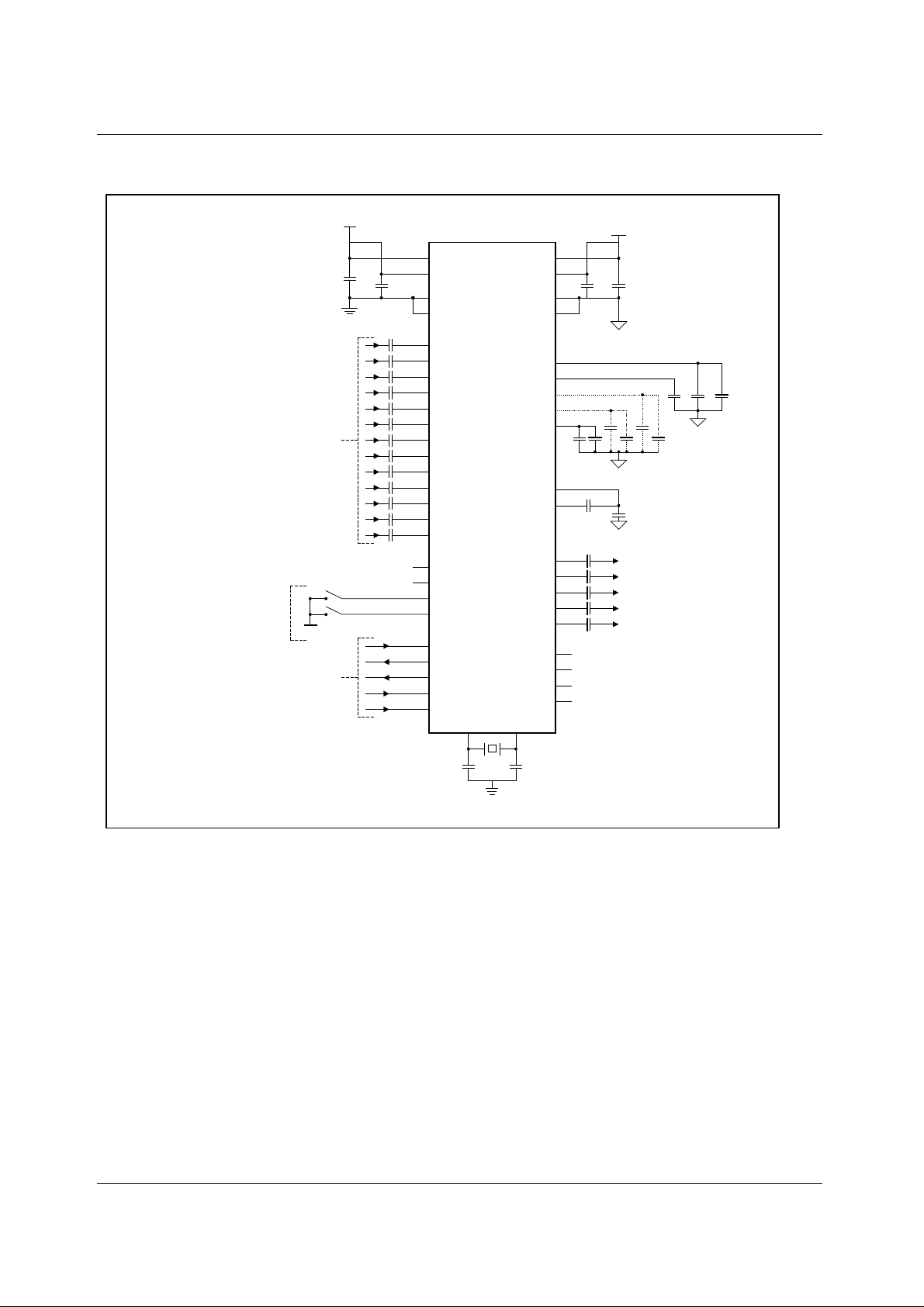
NOTES: 1. Pins 27, 29 and 31 are
internally connected.
It is recommended that
capacitors only be
connected to one of
these pins.
2. C1 to C28 should be as
close to WM9704Q as
possible.
3. AGND and DGND should
be connected as close to
WM9704Q as possible.
MIXER
INPUTS
AVSS
AC-LINK
DVDD
C1
DGND
AVDD
1
DVDD1
9
DVDD2
C2
C5
C6
C7
C8
C9
C10
C11
C12
C13
C14
C15
C16
C17
4
7
12
13
14
15
16
17
18
19
20
21
22
23
24
30
40
46
45
5
6
8
10
11
DVSS1
DVSS2
PCBEEP
PHONE
AUXL
AUXR
VIDEOL
VIDEOR
CDL
CDGND
CDR
MIC1
MIC2
LINEINL
LINEINR
NC
NC
CID1
CID2
SDATAOUT
BITCLK
SDATAIN
SYNC
RESETB
XTLIN
2
C34
WM9703
LINEOUTR
MONOOUT
LNLVLOUTL
LNLVLOUTR
XTLOUT
3
XT
AVDD1
AVDD2
AVSS1
AVSS2
VREF
VREFOUT
AFILT1
CAP1
CAP2
CX3D1
CX3D2
LINEOUTL
EAPD
C35
25
38
C3 C4
26
42
AGND
27
28
29
31
32
C23 C25
C21 C22
+
C24 C26
33
34
35
36
37
39
41
43
NC
44
NC
48
NC
47
AGND
C27
AGND
C29
+
++
C30
+
C31
+
C32
+
C33
+
C18 C19 C20
++
C28
AGND
STEREO OUTPUT
MONO OUTPUT
LINE LEVEL STEREO
+
DGND
Figure 19 External Components Diagram
WOLFSON MICROELECTRONICS LTD PD Rev 3.4 January 2001
28
Page 29

Production Data WM9703
RECOMMENDED EXTERNAL COMPONENTS VALUES
COMPONENT
REFERENCE
C1 to C4 10nF De-coupling for DVDD and AVDD
C5 to C17 470nF AC coupling capacitors for setting DC level of analogue inputs to VCA P1.
C18 1µF
C19 0.1µF
C20 10µF
C21 0.1µF
C22 10µF
C23 0.1µF
C24 10µF
C25 0.1µF
C26 10µF
C27 100nF 3D low pass filter. This value sets nom i nal 100Hz.
C28 47nF 3D high pass fil ter. This value sets nominal 1kHz.
C29 to C33 10µF Output AC coupling caps to remove VREF DC level from outputs.
C34 and C35 22pF Optional capacit ors for better crystal frequency stabilit y.
XT 24.576 MHz AC’97 master clock frequency. A bias resistor is not required, but if connected will not
Table 24 External Component Values
SUGGESTED
VALUE
DESCRIPTION
Value chosen to give corner frequenc y below 20Hz for min 10K input impedanc e.
Reference de-coupling capacit ors for ADC, DAC, Mixer and CAP2 references .
Ceramic type or sim i l ar.
affect operation if value i s large (above 1MΩ).
RECOMMENDATIONS FOR 3.3V OPERATION
The device’s performance with AVDD = 3.3V is shown in Electrical Characteristics.
In 3.3V analogue operation, mi d-rai l reference scales to 1.5V . All ADC and DAC references are 3/ 5
of their nominal 5V value. Input and output signals that are 1Vrms in 5V applications, scale to
660mVrms in 3.3V applications . If 1Vrms output is required, the m ixer gain adjust PGAs need to be
increased by 3 times 1. 5dB steps.
ths
WOLFSON MICROELECTRONICS LTD PD Rev 3.4 January 2001
29
Page 30
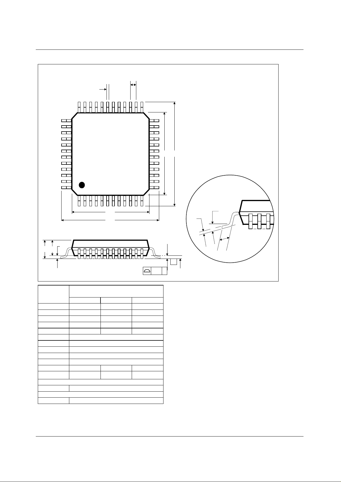
WM9703 Production Data PACKAGE DIMENSIONS
FT: 48 PIN TQFP (7 x 7 x 1.4 mm)
b
48
D1
D
DM003.B
e
2536
2437
E1 E
13
121
θ
c
A1
A
A2
-C-
SEATING PLANE
C
ccc
Dimensions
Symbols
(mm)
MIN NOM MAX
A
A
1
A
2
----- ----- 1.60
0.05 ----- 0.15
1.35 1.40 1.45
b 0.17 0.22 0.27
c
D
D
1
0.09 ----- 0.20
9.00 BSC
7.00 BSC
E 9.00 BSC
E
1
e
L
θ
0.45 0.60 0.75
o
0
7.00 BSC
0.50 BSC
o
3.5
o
7
Tolerances of Form and Position
ccc
0.08
REF: JEDEC.95, MS-026
NOTES:
A. ALL LINEAR DIMENSIONS ARE IN MILLIMETERS.
B. THIS DRAWING IS SUBJECT TO CHANGE WITHOUT NOTICE.
C. BODY DIMENSIONS DO NOT INCLUDE MOLD FLASH OR PROTRUSION, NOT TO EXCEED 0.25MM.
D. MEETS JEDEC.95 MS-026, VARIATION = BBC. REFER TO THIS SPECIFICATION FOR FURTHER DETAILS.
L
WOLFSON MICROELECTRONICS LTD PD Rev 3.4 January 2001
30
 Loading...