

Page 1
WM8720
24-bit, 96kHz Stereo DAC with Volume Control
Production Data, November 2000, Rev 3.0
DESCRIPTION
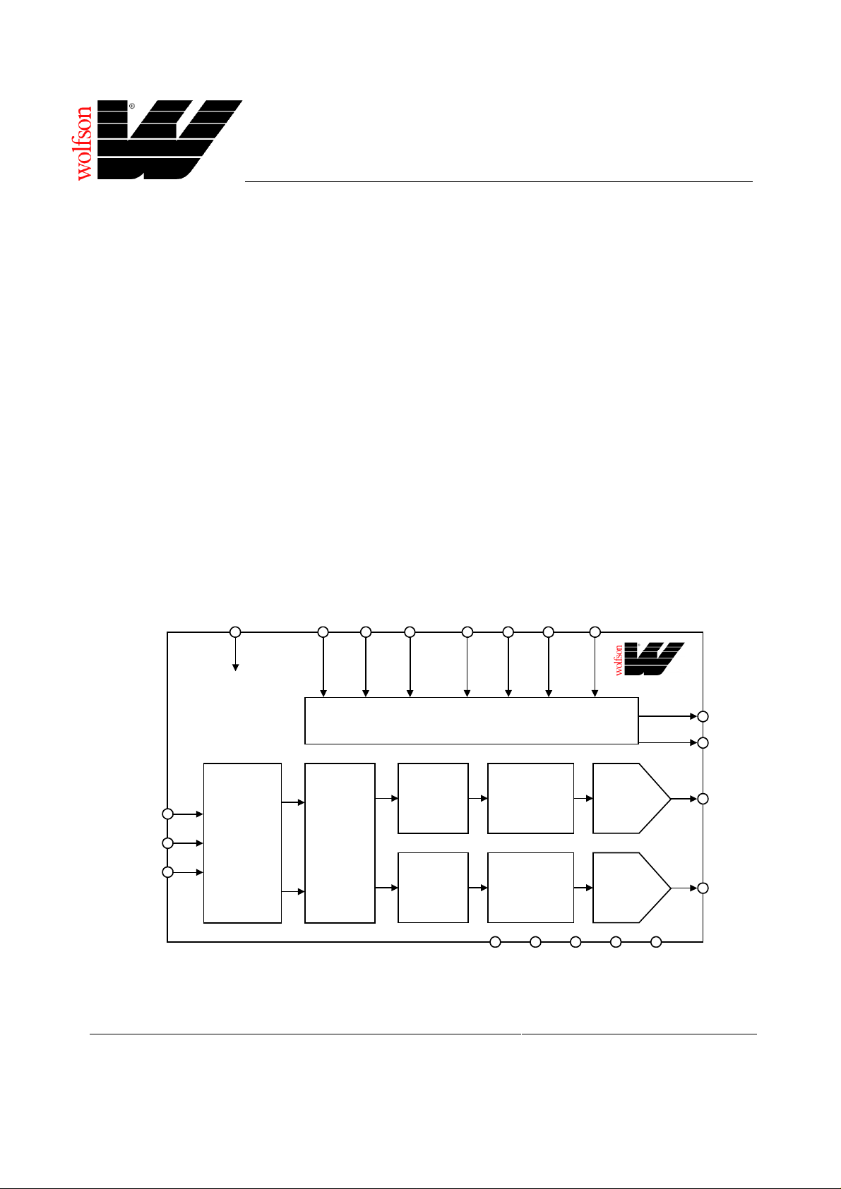
The WM8720 is a high perform ance stereo DAC desi gned
for audio applications such as CD, DVD, home theatre
systems, set top boxes and digital TV. The WM8720
supports data input word lengths from 16 to 24-bits and
sampling rates up to 96kHz. The WM8720 consists of a
serial interface port, digital interpolation filter, multi-bit
sigma delta modulator and stereo DAC in a small 20-pin
SSOP package. The WM8720 also includes a digitally
controllable mute and att enuator function on each channel.
The WM8720 supports a variet y of connect ion s chem es f or
audio DAC control. The SPI-compat ible serial control port
provides access to a wide range of feat ures including onchip mute, attenuation and phase reversal. A hardware
controllable interface is also available.
The programmable data input port supports a variety of
glueless interfaces to popular DSPs, audio decoders and
S/PDIF and AES/EBU receivers.
BLOCK DIAGRAM
MC/IWL
SCKI
(2)
ML/I2S
(4)
(5)
FEATURES
• Performance:
- 102dB SNR (‘A’ weighted @48kHz),
- THD: -95dB @ 0dB FS
• 5V or 3.3V supply operation
• Sampling frequency: 8kHz to 96kHz
• Input data word: 16 to 24-bit
• Hardware or SPI compatible seri al port control modes:
- Hardware mode: system clock, reset, mut e,
de-emphasis
- Serial control mode: mute, de-emphasis, digital
attenuation (256 steps), zero mute, phase reversal,
power down
• Compatible with PCM1720
APPLICATIONS
• CD, DVD audio
• Home theatre systems
• Set top boxes
• Digital TV
MD/DM
(6)
PWDN
(1)
RSTB
(7)
MODE
(18)
MUTE
(17)
256fs/384fs
BCKIN (14)
LRCIN (16)
DIN (15)
WOLFSON MICROELECTRONICS LTD
Lutton Court, Bernard Terrace, Edi nburgh, EH8 9NX, UK
Tel: +44 (0) 131 667 9386
Fax: +44 (0) 131 667 5176
Email: [email protected]
http://www.wolfson.co.uk
SERIAL
INTERFACE
DIGITAL
FILTERS
CONTROL INTERFACE
MUTE/
ATTEN
MUTE/
ATTEN
SIGMA
DELTA
MODULATOR
SIGMA
DELTA
MODULATOR
(20)
DGND
AGND
WM8720
DAC
DAC
(10)
(13)
(11)
CAP
AVDD
Production Data Datasheets contain final
specifications current on publication date.
Supply of products conforms to Wol fson
Microelectronics’ Term s and Conditions.
2000 Wolfson Microelectronics Ltd.
(19)
DVDD
(3) TEST
(8) ZERO
(9) VOUTR
(12) VOUTL
Page 2
WM8720 Production Data
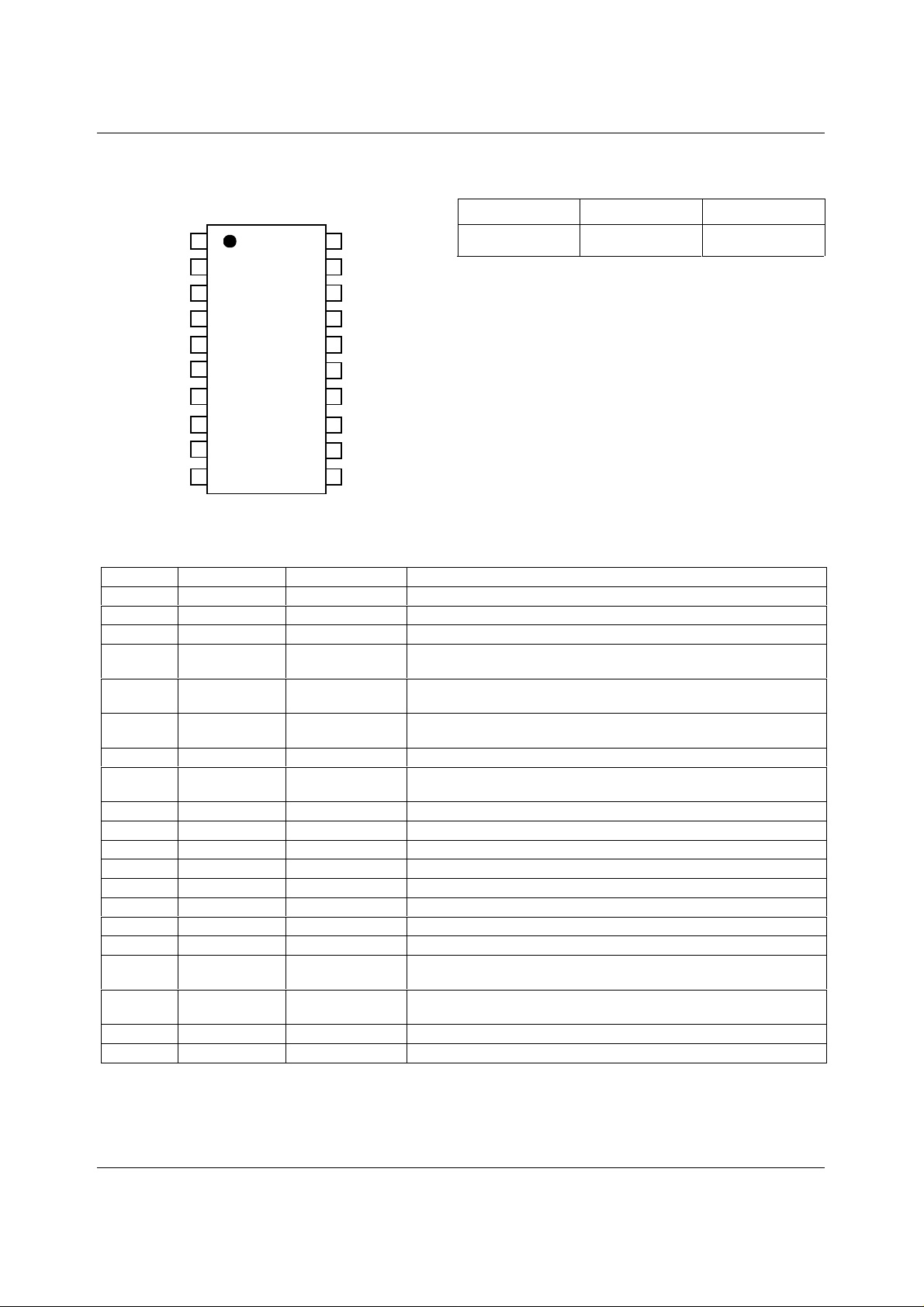
PIN CONFIGURATION ORDERING INFORMATION
DEVICE TEMP. RANGE PACKAGE
PWDN
SCKI
TEST
ML/I2S
MC/IWL
MD/DM
RSTB
ZERO
VOUTR
AGND
1
2
3
4
5
6
7
8
9
10
20
19
18
17
16
15
14
13
12
11
DGND
DVDD
MODE
MUTE
LRCIN
DIN
BCKIN
CAP
VOUTL
AVDD
WM8720EDS -25 to +85oC 20-pin SS OP
PIN DESCRIPTION
PIN NAME TYPE DESCRIPTION
1 PWDN Digital input
2 SCKI Digital input
3 TEST Digital output
4 ML/I2S Digital input
5 MC/IWL Digital input
6 MD/DM Digital input
7 RSTB Digi t al i nput
8 ZERO Digital output
9 VOUTR Analogue output
10 AGND Supply
11 AVDD Supply
12 VOUTL Analogue output
13 CA P Analogue out put
14 BCKIN Digital i nput
15 DIN Digital input
16 LRCIN Digital input
17 MUTE Digital IO
18 MODE Digital input
19 DVDD Supply
20 DGND Supply
Note:
Digital input pins have Schmitt trigger input buffers.
Powerdown control; low is ON, high is POWER OFF. Internal pull-down.
System clock i nput (256 or 384fs).
Reserved.
Latch enable (software mode) or input f ormat selection (hardware mode).
Internal pull-up.
Serial control data cloc k input (software mode) or input word length
selection (hardware mode). Internal pul l -up.
Serial control data input (s of tware mode) or de-emphasis selec tion
(hardware mode). Internal pull-up.
Reset input – active low. Internal pull-up.
Infinite zero detect – active low. Open drain type output with active
pull-down.
Right channel DAC output.
Analogue ground supply.
Analogue positive supply.
Left channel DAC output.
Analogue internal reference.
Audio data bit clock i nput .
Serial audio data input.
Sample rate clock i nput.
Mute control pin, input or automute output.
Low is not mute, high is mute, Z is automute.
Mode select pin. Low is software mode, high is hardware control.
Internal pull-down.
Digital positive supply.
Digital ground supply.
WOLFSON MICROELECTRONICS LTD PD Rev 3.0 November 2000
2
Page 3
Production Data WM8720
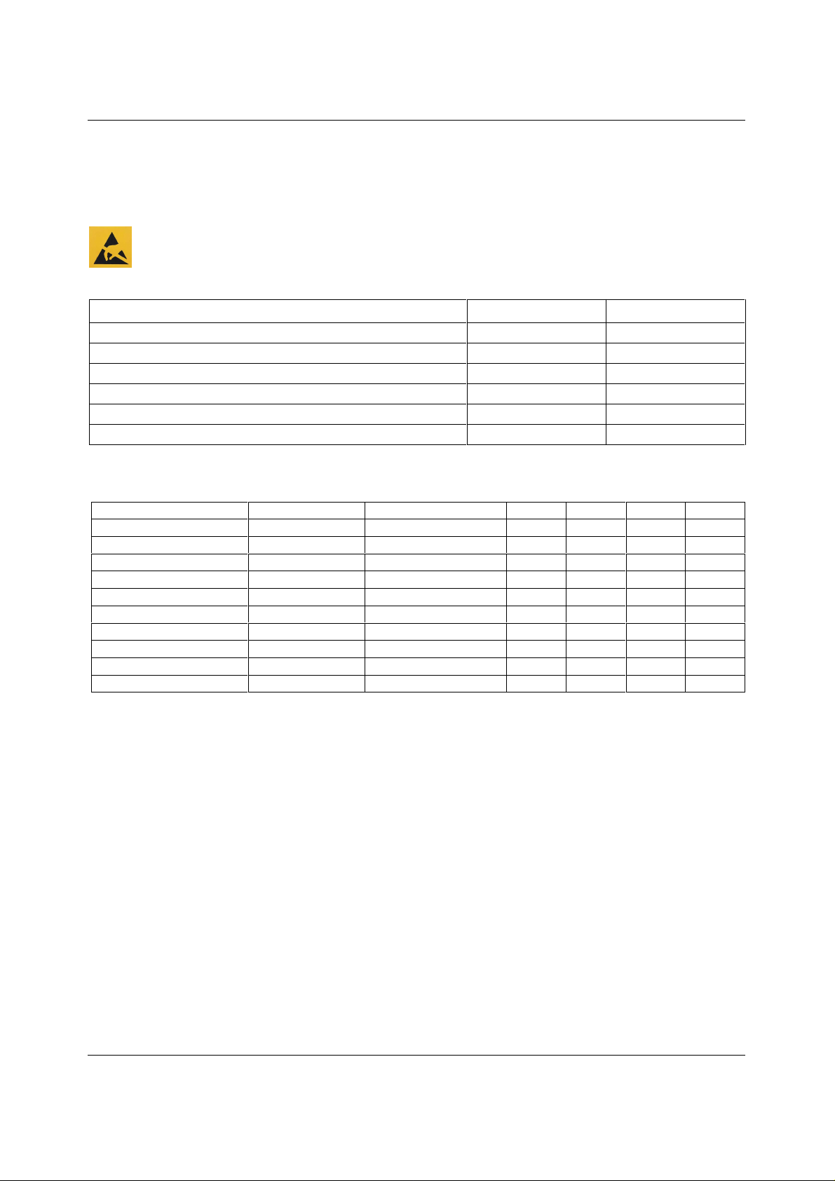
ABSOLUTE MAXIMUM RATINGS
Absolute Maximum Ratings are s tres s rat ings only. P erm anent damage to the device may be c aused by c onti nuously operat ing at
or beyond these limits. Device functional operating lim its and guaranteed performance s pecifications are gi ven under Electrical
Characteristics at the test conditions s pecified.
ESD Sensitive Device. Thi s device i s m anufactured on a CMOS process . It i s t herefore generi cally suscept ible
to damage from excessi ve stati c voltages . Proper ES D precautions mus t be tak en during handling and st orage
of this device.
CONDITION MIN MAX
Supply voltage
Reference input
Operating temperature range, T
A
Storage temperature
Package body temperature (s ol deri ng, 10 seconds)
Package body temperature (s ol deri ng, 2 minutes)
-0.3V +7V
VDD + 0.3V
+240
+183
o
C
o
C
o
C
-25oC+85
o
-65
C +150oC
RECOMMENDED OPERATING CONDITIONS
PARAMETER SYMBOL TEST CONDITIONS MIN TYP MAX UNIT
Digital supply range
Analogue supply range
Ground
Difference DGND to AGND
Analogue supply current
Digital supply current
Analogue supply current
Digital supply current
Standby analogue current
Standby digital current
DVDD -10% 3.3 to 5 +10% V
AVDD -10% 3.3 to 5 +10% V
AGND, DGND 0 V
-0.3 0 +0.3 V
AVDD = 5V 17 mA
DVDD = 5V 6 mA
AVDD = 3.3V 16 mA
DVDD = 3.3V 3 mA
AVDD = 5V 1.7 mA
DVDD = 5V 30 µA
WOLFSON MICROELECTRONICS LTD PD Rev 3.0 November 2000
3
Page 4
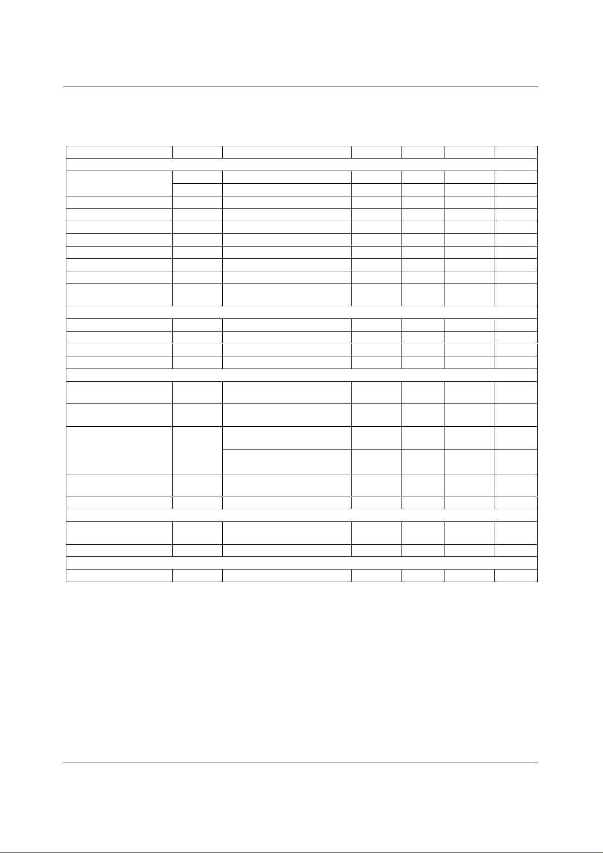
WM8720 Production Data ELECTRICAL CHARACTERISTICS
Test Conditions
AVDD, DVDD = 5V, AGND, DGND = 0V , T
PARAMETER SYMBOL TEST CONDITIONS MIN TYP MAX UNIT
DAC Circuit Specifications
SNR (Note 1)
THD
Dynamic range
Passband
Stopband
Pass band ripple
Out of band rejection
Channel Separation
Gain mismatch
channel-to-channel
Digital Logic Levels
Input LOW level
Input HIGH level
Output LOW level
Output HIGH level
V
IL
V
IH
V
OL
V
OH
Analogue Output Levels
Output level
Minimum resist ance load
Maximum capacitance
load
Output DC level
Reference Levels
Potential divider
resistance
Voltage at CAP
POR
POR threshold
= +25oC, fs = 48kHz, SCKI = 256f s unless otherwise stated.
A
AVDD, DVDD = 5V 95 102 dB
AVDD, DVDD = 3.3V 100 dB
0dB FS -96 -85 dB
THD+N @ -60dB FS 95 102 dB
±0.25dB 0.4535 fs
-3dB 0.491 fs
±0.25 dB
-40 dB
98 dB
0dB FS ±0.5 ±5 %FSR
0.8 V
2.0 V
IOL = 2mA AV
SS
+ 0.3V
IOH = 2mA AVDD - 0.3V
Into 10kohm, full scale 0dB,
1.1 V
(5V supply)
Into 10kohm, full scale 0dB,
0.72 V
(3.3V supply)
To midrail or AC coupled
1 kohms
(5V supply)
To midrail or AC coupled
1 kohms
(3.3V supply)
5V or 3.3V 100 pF
AVDD/2 V
AVDD to CAP and CAP to AGND
90 kohms
AVDD/2
2.0 V
RMS
RMS
TERMINOLOGY
1. Signal-to-noise ratio (dB) (SNR) i s a measure of the difference in level between the full-scale output and the output
with no signal applied.
2. Dynamic range (dB) (DNR) is a m easure of the difference between the highest and l o west portions of a signal.
Normally a THD+N measurem ent at 60dB below full scale. The measured signal is then correct ed by addi ng the 60dB
to it. (eg THD+N @ -60dB= -32dB, DR= 92dB).
3. THD+N (dB) is a ratio of the r.m.s. values, of (Nois e + Di stortion)/Signal.
4. Stop band attenuation (dB) is t he degree to which the frequency spectrum i s attenuated (outside audio band).
5. Channel Separation (dB) (also known as Cross -Tal k) is a measure of the amount one channel is isolated f rom the
other. Normally measured by sending a full-scale signal down one channel and measuring the other.
6. Pass-Band Ripple - Any variati on of the frequency response in the pass-band region.
WOLFSON MICROELECTRONICS LTD PD Rev 3.0 November 2000
4
Page 5
Production Data WM8720
LRCIN
t
BCH
t
BCL
t
LB
BCKIN
t
BCY
t
BL
DIN
t
DS
t
DH
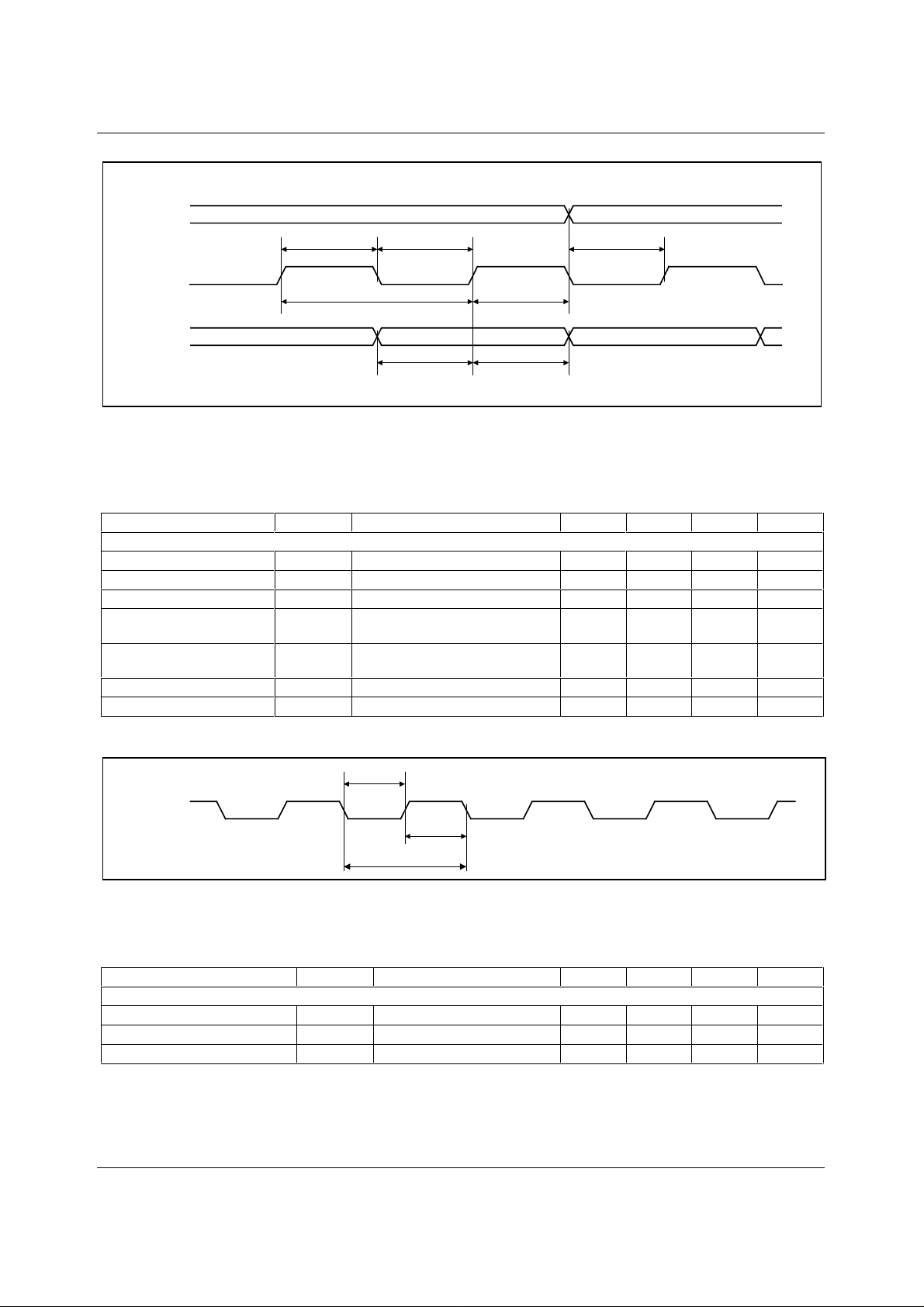
Figure 1 Audio Data Input Timing
Test Conditions
AVDD, DVDD = 5V, AGND, DGND = 0V , T
= +25oC, fs = 48kHz, SCKI = 256f s unless otherwise stated.
A
PARAMETER SYMBOL TEST CONDITIONS MIN TYP MAX UNIT
Audio Data Input Timing Information
BCKIN pulse cycle time
BCKIN pulse width high
BCKIN pulse width low
BCKIN rising edge to
t
t
t
BCY
BCH
BCL
t
BL
100 ns
40 ns
40 ns
20 ns
LRCIN edge
LRCIN rising edge to
t
LB
20 ns
BCKIN rising edge
DIN setup time
DIN hold time
t
DS
t
DH
20 ns
20 ns
t
SCKIL
SCKI
t
SCKIH
t
SCKY
Figure 2 System Clock Timing Requirements
Test Conditions
AVDD, DVDD = 5V, AGND, DGND = 0V , T
= +25oC, fs = 48kHz, SCKI = 256f s unless otherwise stated.
A
PARAMETER SYMBOL TEST CONDITIONS MIN TYP MAX UNIT
System Clock Timing Information
System clock pul se width high
System clock pul se width low
System clock cycle time
t
SCKIH
t
SCKIL
t
SCKY
10 ns
10 ns
27 ns
WOLFSON MICROELECTRONICS LTD PD Rev 3.0 November 2000
5
Page 6
WM8720 Production Data
t
MLS
t
t
MLL
MLH
ML/12S
t
MCH
t
MCL
MC/IWL
t
MCY
MD/DM
t
MDS
t
MDH
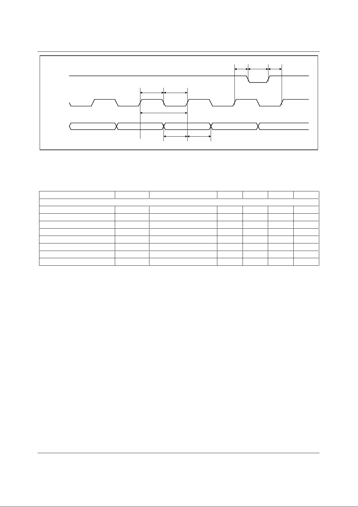
Figure 3 Program Register Input Timing
Test Conditions
AVDD, DVDD = 5V, AGND, DGND = 0V , T
= +25oC, fs = 48kHz, SCKI = 256f s unless otherwise stated.
A
PARAMETER SYMBOL TEST CONDITIONS MIN TYP MAX UNIT
Program Register Input Information
MC/IWL pulse cycle time
MC/IWL pulse width low
MD/DM pulse width high
MD/DM set-up time
MC/IWL hold time
ML/I2S pulse width low
ML/I2S set-up time
ML/I2S hold time
t
t
t
t
t
t
t
t
MCY
MCL
MCH
MDS
MDH
MLL
MLS
MLH
100 ns
40 ns
40 ns
20 ns
20 ns
20 ns
20 ns
20 ns
Notes:
1. Ratio of output level with 1kHz ful l scale input, to the output l evel with all zeros into the digital input , measured “A”
weighted over a 20Hz to 20kHz bandwidth.
2. All performance measurements done with 20kHz low pass filter. Failure to use such a f ilt er will result in higher
THD+N and lower SNR and Dynamic Range readings than are found in the Electrical Characteri stics. The low
pass filter removes out of band noise; although it is not audible it may affect dynamic specif ication values.
WOLFSON MICROELECTRONICS LTD PD Rev 3.0 November 2000
6
Page 7

Production Data WM8720
DEVICE DESCRIPTION
WM8720 is a complete s tereo audio digit al-to-analogue c onverter, inc luding digit al interpolat ion filt er,
multibit sigm a delta with dither, switched c apacitor mult ibit stereo DAC and out put smoothing f ilters.
Control of internal functionality of the device is by either hardware control (pin programmed) or
software control (serial interf ace). The MODE pin sel ects between hardware and software c ontrol. In
software control mode, an SPI type interf ace is used. This interface may be asynchronous to the
audio data interface. Control data will be re-synchronized to the audio processing internally.
The device is pin compati ble with the PCM1720, but uses additional pins that are not used on t hat
device to achieve greater user flexibility.
Operation using system c lock of 256fs or 384fs is provided. S election between cloc k rates is being
automatically controll ed in hardware mode, or serial controlled when in sof tware mode. S ample rat es
(fs) from less than 8ks/s to 96ks/ s are allowed, provided the appropriate system clock is input.
The data interface supports norm al (Japanese right justified) and I
delayed) interface format s, in both ‘packed’ and unpacked forms . W hen in hardware m ode, the three
serial interface pins bec ome control pins to allow s election of input data form at type (I
input word length (16, 18, 20, or 24-bit) and de-emphasis function.
SYSTEM CLOCK
The system clock for WM8720 must be either 256fs or 384fs, where fs is the audio sampling
frequency (LRCIN) typically 32kHz, 44.1kHz, 48 or 96kHz. The syst em clock is used to operate the
digital filters and the noi se shaping circuits.
WM8720 has a system cloc k detec tion ci rcuitry t hat aut omati cally determ ines what the s ystem c lock
frequency relative to the sam pling rate is (to within ±8 system clocks). If greater than 8 clocks error,
then the interface shuts down the DAC and mutes the output. The system clock should be
synchronised with LRCIN, but WM8720 is tolerant of phase di ff erences or jit ter on t his cloc k . Severe
distortion in the phase difference between LRCIN and the system clock will be detect ed, and cause
the device to automati cally resynchronise. If the externally applied LRCIN slips in phase by more
than half the internal LRCIN period, which is derived from master clock, then the interface
resynchronises. Such a c ase would, for exampl e, occ ur if repeated LRCI N clocks were received with
only 252 systems cl ocks per period. In this case the interface would resynchronise every 64 LRCIN
periods. During resynchronisation, the device will either repeat t he previous s ample, or drop the next
sample, depending on the nature of the phase slip. This will ensure no discernible “click “ at the
analogue outputs during resynchronisat ion. Tabl e 1 shows t he typic al sys tem c lock frequenc y i nputs
for the WM8720.
2
S (Philips left justified, one bit
2
S or normal),
SAMPLING RATE (LRCIN)
SYSTEM CLOCK FREQUENCY (MHZ)
256fs 384fs
32kHz 8.192 12.288
44.1kHz 11.2896 16.9340
48kHz 12.288 18.432
96kHz 24.576 36.864
Table 1 System Clock Frequencies Versus Sampling Rate
AUDIO DATA INTERFACE
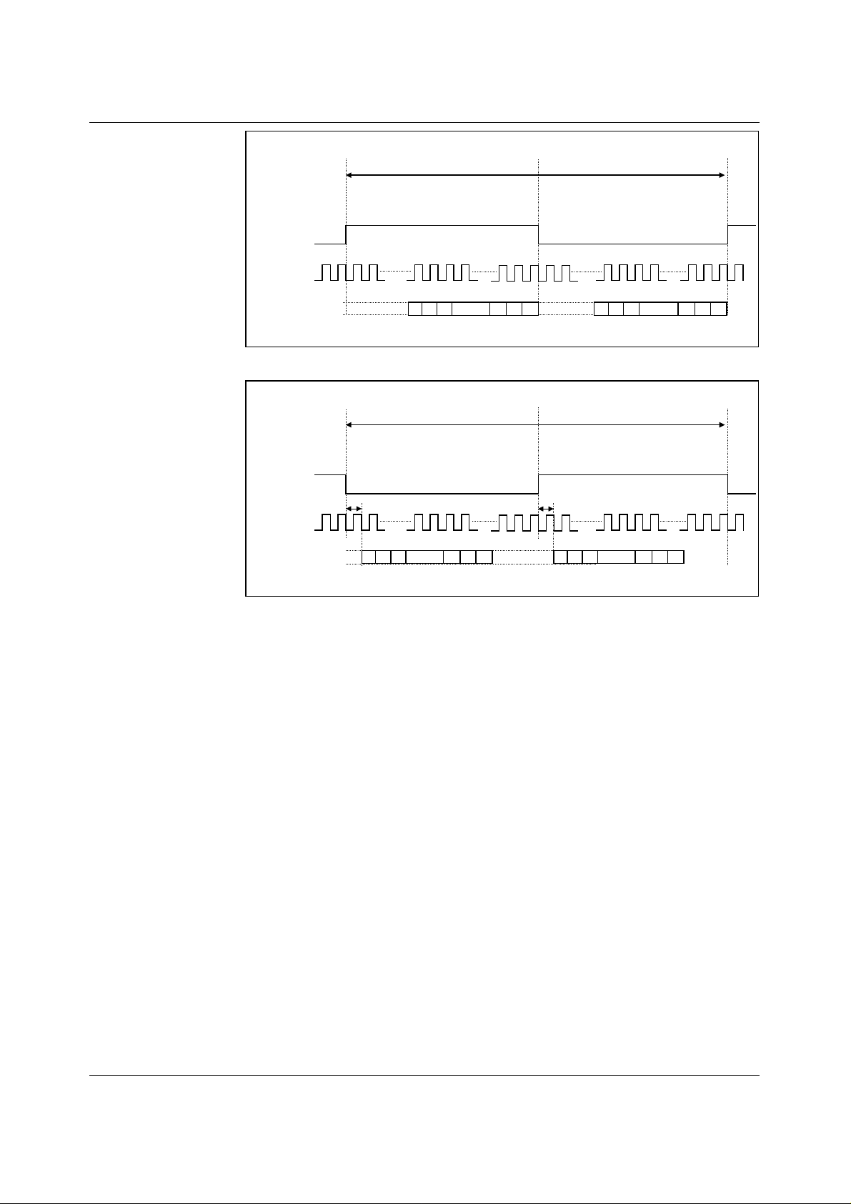
The Serial Data interface to WM8720 is fully compatible with both normal (MSB first, ri ght-justified) or
2
I
S interfaces. Data m ay be ‘packed’ (number of serial bit clocks per LRCIN period is exactly 2 times
the number of data bits, i.e. normally 32 in 16-bit m ode) or unpacked (more than 32 bit clocks per
LRCIN period).
The WM8720 will automatically detect 16-bit packed data being sent to the device in norm al mode,
and accept the data in this i nput format accordingly.
2
I
S MODE DESCRIPTION
0 Normal format (MSB-f i rst, right justif i ed)
1I
Table 2 Serial Interface Formats
WOLFSON MICROELECTRONICS LTD PD Rev 3.0 November 2000
2
S format (Philips serial data protocol )
7
Page 8
WM8720 Production Data
1/fs
LEFT CHANNEL RIGHT CHANNEL
LRCIN
BCKIN
DIN
123
MSB MSB LSB
Figure 4 Normal Data Input Timing
LEFT CHANNEL RIGHT CHANNEL
LRCIN
BCKIN
DIN
123
MSB
Figure 5 I2S Data Input Timing
123
MSB LSBLSB
123
nn-1n-2
nn-1n-2
nn-1n-2
LSB
1/fs
nn-1n-2
WOLFSON MICROELECTRONICS LTD PD Rev 3.0 November 2000
8
Page 9

Production Data WM8720
MODES OF OPERATION
Control of the various modes of operation i s either by software control over the serial interf ace, or
by hard-wired pin control. Selection of software or hardware mode is via MODE pin. The following
functions may be controlled either via the serial control interface or by hard wiring of the
appropriate pins.
FUNCTION
OPTIONS
Input audio
data format
Normal format
2
I
S format
Input word length 16
18
20
24
De-emphasis selection On
Off
Mute On
Off
Power down control WM8720 on
WM8720 off
Input LRCIN polarity Lch/Rch = High/low
Lch/Rch = Low/high
Volume control Lch, Rch individually
Lch, Rch common
Infinite zero detect On
Off
Operation enable (OPE) Enabled
Disabled
DAC output control See Table 11
for all options
SOFTWARE CONTROL
DEFAULT VALUE
PIN 18: MODE = 0
2
S = 0 (default)
I
2
I
S = 1
IW[1:0] = 00 (default)
IW[1:0] = 11
IW[1:0] = 01
IW[1:0] = 10
DE = 1
DE = 0 (default)
MU = 1
MU = 0 (default)
HARDWARE CONTROL
BEHAVIOUR
PIN 18: MODE = 1
2
Pin 4, 5: ML/ I
Pin 4, 5: ML/I
Pin 4, 5: ML/I2S, MC/IWL = 00
Pin 4, 5: ML/I
Pin 4, 5: ML/I
Pin 4, 5: ML/I
S, MC/IWL =
00 or 01 or 10
2
S, MC/IWL = 11
2
S, MC/IWL = 11
2
S only)
(I
2
S, MC/IWL = 01
2
S, MC/IWL = 10
Pin 6: MD/DM = 1
Pin 6: MD/DM = 0
Pin 17: MUTE = 1
Pin 17: MUTE = 0
Available from Pin 1: P WDN Pin 1: PWDN = 0
Pin 1: PWDN = 1
LRP = 0 (default)
LRP = 1
ATC = 0; 0dB (default)
ATC = 1
IZD = 1
IZD = 0 (default)
OPE = 0 (default)
OPE = 1
Default is PL[3:0] = 1001,
Not available in hardware mode,
default value set
Not available in hardware mode,
default 0dB
Automute functi on controlled
from MUTE pin
Low = not mute
Z = automute enable
High = muted
Not available in hardware mode
stereo mode
Table 3 Control Function Summary
HARDWARE CONTROL MODES
When the MODE pin is hel d hi gh the following hardware modes of operation are available.
MUTE AND AUTOMUTE OPERATION
In both hardware and software modes pin 17 (MUTE) controls selection of mute direct ly, and can be
used to enable and disable the automute function, or as an output of the automuted signal.
WOLFSON MICROELECTRONICS LTD PD Rev 3.0 November 2000
9
Page 10
WM8720 Production Data
IZD (Register Bit)
AUTOMUTED
(Internal Signal)
10k
Ω
MUTE
PIN
MU (Register Bit)
SOFTMUTE
(Internal Signal)
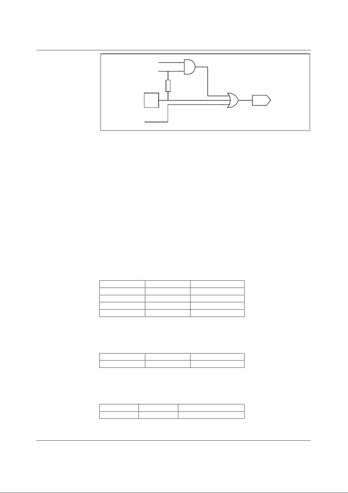
Figure 6 Mute Circuit Operation
The MUTE pin behaves as a bi-directional function, t hat is, as an input to selec t mute or NOT-m ute,
or as an output indication of aut om ute operat ion. MUTE is ac tive hi gh; tak ing t he pi n hi gh c aus es the
filters to soft mute, ramping down the audio signal over a few milliseconds. Taking MUTE low again
allows data into the filter.
The automute function det ects a series of zero value audio samples of 1024 s amples long being
applied to both left and right channels. After such an event, a latch is set whose output (automuted)
is wire OR’ed through a 10kohm resistor to the MUTE pin. Thus i f the MUTE pin is not bei ng driven,
the automute function will assert MUTE.
If MUTE is tied low, automute is overridden and will not mute. If MUTE is driven from a source
follower, or diode, then both mute and automute functions are available. If MUTE is not driven,
automute appears as a weak output (10k source impedance) so can be used to drive external
mute circuits.
The automute signal is AND’ed with IZD, this qualified mute signal then being OR’ed into the
SOFTMUTE control. Therefore, in sof tware mode, automute operation may be control led with IZD
control bit.
I2S INPUT FORMAT SELECTION AND IWL INPUT FORMAT SELECTION
In hardware mode, pins 4 and 5 become input controls for selection of input data format type, and
input data word length, see Table 4. I
enough bit clocks are sent.
2
S – PIN 4 MC/IWL – PIN 5 INPUT DATA MODE
ML/I
0 0 16-bit normal
0 1 20-bit normal
1 0 24-bit normal
11I
Table 4 Control of Input Data Format Type and Input Data Word Length
2
S mode is designed to support any word length provided
2
S mode
DM DE-EMPHASIS
In hardware mode, pin 6 becomes an input control for selection of de-emphasis filtering to be
applied. See Figure 8.
DM 0 De-emphasis off
DM 1 De-emphasis on
Table 5 De-emphasis Control
PWDN POWERDOWN CONTROL
In both hardware and software modes, this pin selects powerdown of the entire device when taken
high.
PWDN 0 Device powered up
PWDN 1 Device powered down
Table 6 Powerdown Control
WOLFSON MICROELECTRONICS LTD PD Rev 3.0 November 2000
10
Page 11
Production Data WM8720
SOFTWARE CONTROL INTERFACE
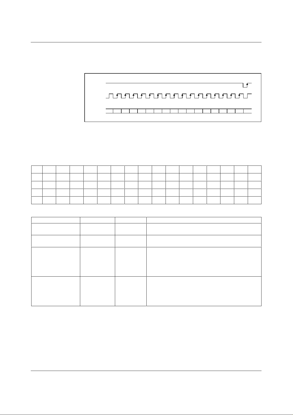
The WM8720 can be controlled using a 3-wire serial interface. MD/DM (pin 6) is used for the program
data, MC/IWL (pin 5) is used to clock in the program dat a and ML/I2S (pin 4) is use to latch i n the
program data. The 3-wire interface protoc ol i s shown in Figure 7.
ML/I2S
MC/IWL
MD/DM
D15 D6D7D8D9D10D11D12D13D14 D1D2D3D4D5 D0
Figure 7 3-Wire Serial Interface
REGISTER MAP
WM8720 controls the special functions using 4 program registers, which are 16-bits long. These
registers are all loaded through input pin MD/DM. After the 16 data bit s are c loc ked i n, ML/I 2S/I WL is
used to latch in the data to t he appropriate register. Table 7 shows the com plete mapping of the
4 registers.
B15 B14 B13 B12 B11 B10 B9 B8 B7 B6 B5 B4 B3 B2 B1 B0
M0
------A1A0LDLAL7AL6AL5AL4AL3AL2AL1AL0
M1
-----A1A0LDRAR7AR6AR5AR4AR3AR2AR1AR0
M2
-----A1A0PL3PL2PL1PL0IW1IW0OPEDEMU
M3
-----A1A0IZDSF1SF0---ATCLRPI
Table 7 Mapping of Program Registers
REGISTER NAME BIT NAME DEFAULT DESCRIPTION
Register 0 (M0)
A[1:0] = 00
Register 1 (M1)
AR[7:0]
A[1:0] = 01
Register 2 (M2)
A[1:0] = 10
IW[1:0]
Register 3 (M3)
A[1:0] = 11
SF[1:0]
Table 8 Internal Register Mapping
AL[7:0]
LDL
LDR
MU
DE
OPE
PL[3:0]
I2S
LRP
ATC
IZD
1111 1111
0
1111 1111
0
0
0
0
00
1001
0
0
0
00
0
DAC attenuation data for left channel
Attenuation data load control for left channel
DAC attenuation data for right channel
Attenuation data load control for right channel
Left and right DACs soft mute control
De-emphasis control
Left and right DACs operation c ont rol
Input audio word resolution
DAC output control
Audio data format select
Polarity of LRCIN (pin 7) select
Attenuator control
Sampling rate select
Infinite zero detection circuit control and automute control
2
S
DAC OUTPUT ATTENUATION
Register 0 (A[1:0] = 00) is us ed to control left channel attenuation. Bit s 0-7 (AL[7:0]) are used to
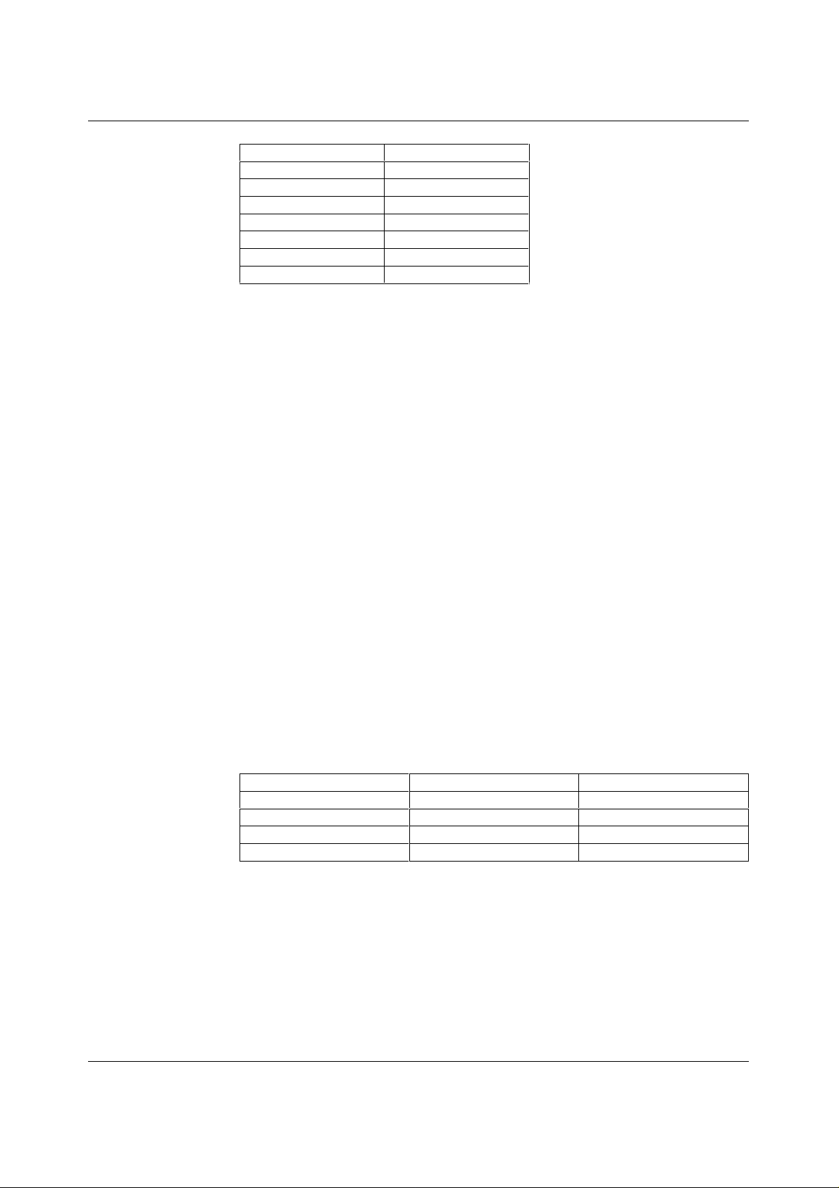
determine the attenuation l evel Tabl e 9. The level of attenuation is given by:
Attenuation = [20.log10 (At t enuation_Data/256)] dB
...................................................................................................
WOLFSON MICROELECTRONICS LTD PD Rev 3.0 November 2000
Eqn. 1
11
Page 12
WM8720 Production Data
AX[7:0] ATTENUATION LEVEL
00(hex) - ∞dB (mute)
01(hex) -48.16dB
::
::
::
Fe(hex) -0.07dB
FF(hex) 0dB
Table 9 Attenuation Control Levels
Bit 8 in register 0 (LDL) is us ed to c ontrol t he loading of at tenuat ion data in AL[ 7:0] . When LDL is set
to 0, attenuation data will be loaded into AL[7:0], but it will not affect the attenuat ion level until LDL is
set to 1. LDR in register 1 has the same function for ri ght channel attenuation.
Register 1 (A[1:0] = 01) is used to control right channel attenuation in a similar manner.
Bit 2 in register 3 (A1[1:0] = 11) is used to control the attenuat or (ATC). When ATC is high, the
attenuation data loaded in program regis ter 0 is used for bot h the left and the right c hannels. W hen
ATC is low, the attenuation dat a for each register is applied separately to left and right channels .
LEFT AND RIGHT DACS SOFT MUTE CONTROL
Soft mute is controlled by setting bit MU, register 2:bit 0. A high level on MU (MU = 1) will cause the
output to be muted, the effect of which is to ramp the s ignal down in the digital dom ain so that t here
is no discernible clic k. This can be seen in Figure 6 Mute Circui t Operation.
DE-EMPHASIS CONTROL
Bit 1 (DE) in register 2 is us ed to control digit al de-emphasis. A low level on bit 1 (DE = 0) disables
de-emphasis whilst a high level enables de-emphasis (DE = 1). De-emphasis applied to the filters
shapes the frequency response of the digital filter acc ordi ng t o t he i nput sample frequency.
LEFT AND RIGHT DACS OPERATION CONTROL
Bit 2 (OPE) in register 2 is used for operation control. W ith OPE = 0 (default) the devic e functions
normally. With OPE = 1 the device is disabled and the outputs are held at midrail. Current
consumption of the digital section is minimized, but analogue sections remain active in order to
preserve DC levels.
INPUT AUDIO WORD RESOLUTION
WM8720 allows maximum flexibility over the cont rol of t he audio dat a interfac e, allowing s election of
format type, word length, and sample rates. B its 3 and 4 of regi st er 2 (IW[1:0]) are used to det erm ine
the input word resolution. WM8720 supports 16-bit, 18-bit, 20-bi t and 24-bit formats as described in
Table 10.
BIT 4 (IW1) BIT 3 (IW0) INPUT RESOLUTION
0 0 16-bit data word
0 1 20-bit data word
1 0 24-bit data word
1 1 18-bit data word
Table 10 Input Data Resolution
WOLFSON MICROELECTRONICS LTD PD Rev 3.0 November 2000
12
Page 13
Production Data WM8720
DAC OUTPUT CONTROL
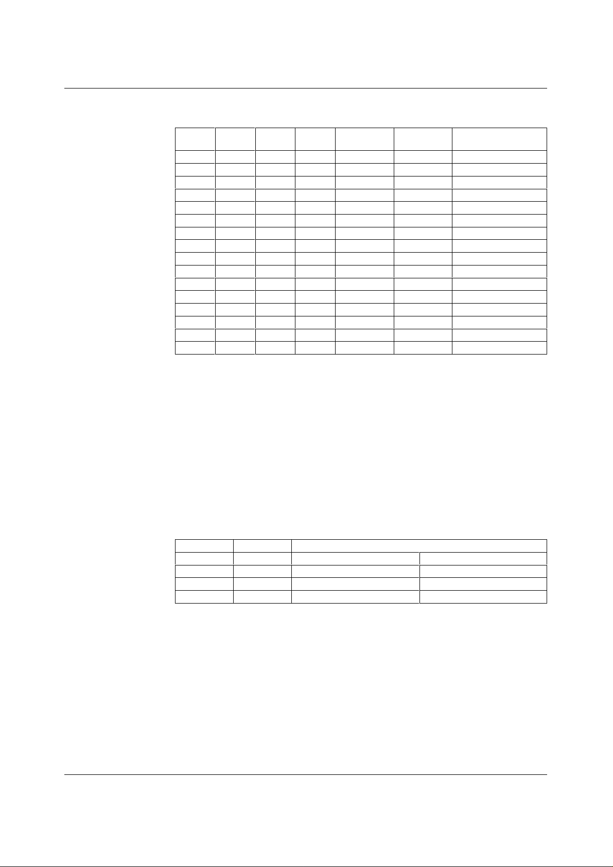
Bits 5, 6, 7 and 8 (PL[3:0]) of register 2 are used to control t he output format as shown in Table 11.
PL3 PL2 PL1 PL0 LEFT
OUTPUT
RIGHT
OUTPUT
NOTE
0 0 0 0 MUTE MUTE Mute bot h channels
0001 L MUTE
0010 R MUTE
0011(L + R)/2MUTE
0100MUTE L
0101 L L
0 1 1 0 R L Reverse channels
0111(L + R)/2 L
1000MUTE R
1 0 0 1 L R Stereo mode
1010 R R
1011(L + R)/2 R
1 1 0 0 MUTE (L + R)/2
1101 L (L + R)/2
1110 R (L + R)/2
1 1 1 1 (L + R)/2 (L + R)/2 Mono mode
Table 11 Programmable DAC Output Format
SERIAL PROTOCOL
Bits 0 (I2S) and 1 (LRP) of register 3 are used to c ontrol the input data form at com pletely. A low on
2
bit 0 (I
S = 0) sets the format to Normal (MSB-first, right just ified Japanese format), whilst a high
2
S = 1) sets the format to I2S (Philips serial data protocol).
(I
POLARITY OF LRCIN SELECT
Bit 1 (LRP) of register 3 is used to cont rol the polarity of LRCIN (sam ple rate clock). W hen bit 1 is
low (LRP = 0), left channel data is assumed when LRCIN is in a high phase and right channel data
is assumed when LRCIN is in a l ow phase. When bit 1 is high (LRP = 1), the polarity assumption
is reversed.
INTERFACE CLOCKS AND SAMPLING RATES
Bits 6 (SF0) and 7 (SF1) of register 3 are used to control the sampling frequency, as shown in
Table 12.
SF0 SF1 SAMPLING FREQUENCY
0 0 44.1 kHz group 22.05 / 44.1 / 88.2 kHz
0 1 48 k Hz group 24 / 48 / 96 kHz
1 0 32 k Hz group 16 / 32 / 64 kHz
1 1 Reserved Not defined
Table 12 Sampling Frequencies
INFINITE ZERO DETECTION
Bit 8 (IZD) in register 3 controls operat ion of the automute function. If IZD (Infinite Zero Detect) is
high, 1024 consecutive zero audio samples will force t he output to zero. See Figure 6. Note that the
control of pin MUTE also affect s automute operat ion. To turn off automute, pin MUTE mus t be held
low as well as IZD being low (default).
WOLFSON MICROELECTRONICS LTD PD Rev 3.0 November 2000
13
Page 14
WM8720 Production Data RECOMMENDED EXTERNAL COMPONENTS
DVDD
+
C
1
DGND
Software I/F or
Hardware Control Pins
Audio Serial Data I/F
NOTES: 1. AGND and DGND should be connected as close to the WM8720 as possible.
, C3 and C7 should be positioned as close to the WM8720 as possible.
2. C
2
3. Capacitor types should be carefully chosen. Capacitors with very low ESR are
recommended for optimum performance.
19
DVDD
C
2
20
DGND
4
ML/I2S
5
MC/IWL
6
MD/DM
7
RSTB
18
MODE
1
PWDN
17
MUTE
2
SCKI
14
BCKIN
15
DIN
16
LRCIN
AVDD
AGND
VOUTR
VOUTL
ZERO
TEST
CAP
10
C3C
11
9
12
8
3
13
C
AVDD
+
4
AGND
C
5
+
C
6
+
AVDD
C
8
7
AGND
AC-Coupled
Output to
External LPF
R1
+
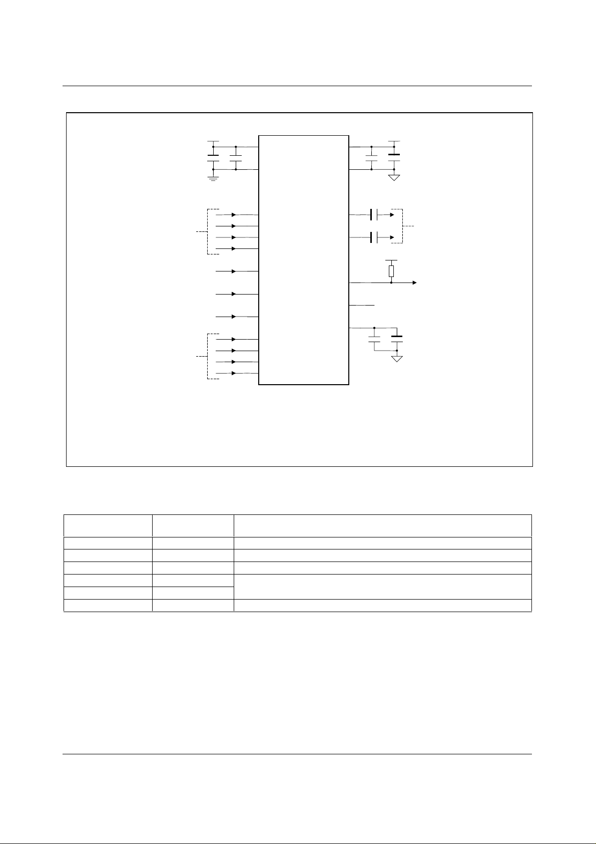
Figure 8 External Components Diagram
RECOMMENDED EXTERNAL COMPONENTS VALUES
COMPONENT
REFERENCE
C1 and C4 10µF
C2 and C3 0.1µF
C5 and C6 10µF
C7 0.1µF
C8 10µF
R1 10kΩ
Table 13 External Components Description
WOLFSON MICROELECTRONICS LTD PD Rev 3.0 November 2000
SUGGESTED
VALUE
DESCRIPTION
Output AC coupling caps t o remove midrail DC level from outputs.
Reference de-coupling capacit ors for CAP pin.
Resistor to AVDD for open drain output operation.
14
Page 15
Production Data WM8720
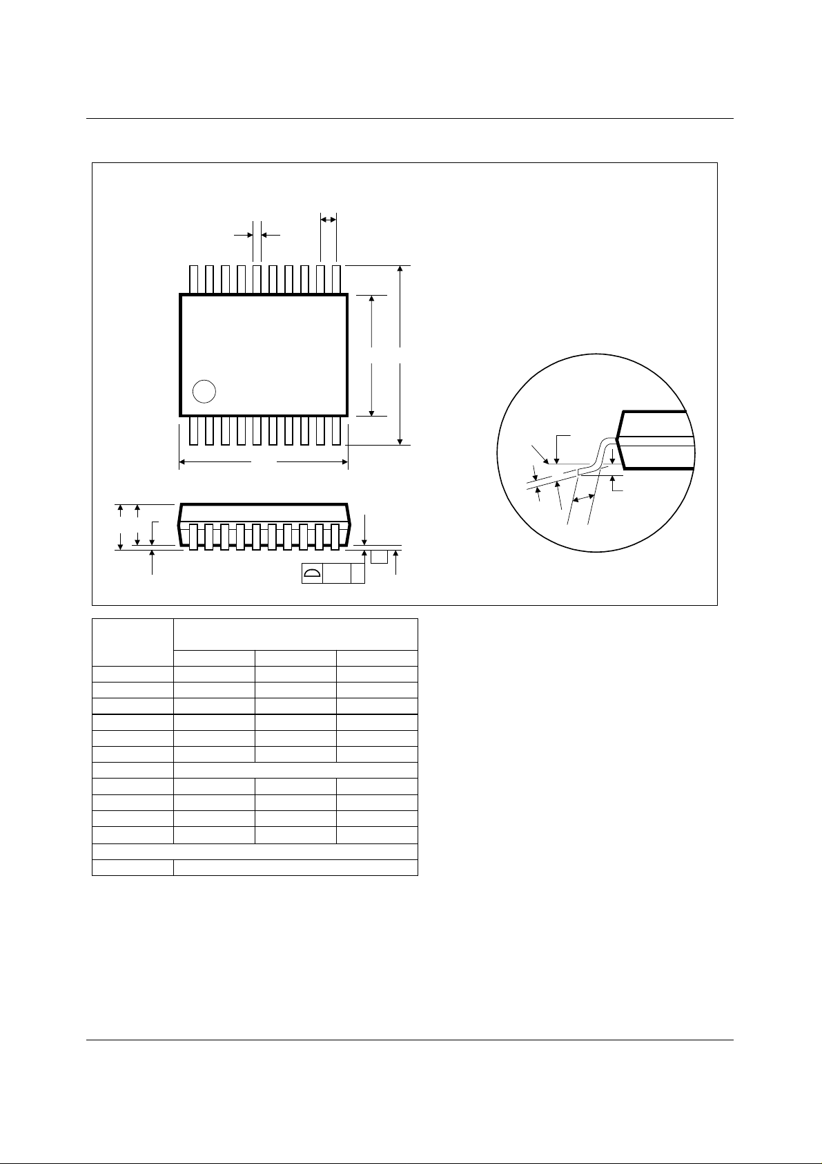
PACKAGE DIMENSIONS
DM0015.ADS: 20 PIN SSOP (7.2 x 5.3 x 1.75 mm)
b
D
A2
A1
A
e
101
0.10
1120
C
Dimensions
Symbols
(mm)
MIN NOM MAX
A
A
1
A
2
----- ----- 2.0
0.05 ----- -----
1.65 1.75 1.85
b 0.22 ----- 0.38
c
D
e
E
E
1
L
θ
0.09 ----- 0.25
6.90 7.20 7.50
0.65 BSC
7.40 7.80 8.20
5.00 5.30 5.60
0.55 0.75 0.95
o
0
o
4
E1 E
-C-
SEATING PLANE
o
8
GAUGE
PLANE
Θ
0.25
c
L
REF: JEDEC.95, MO-150
NOTES:
A. ALL LINEAR DIMENSIONS ARE IN MILLIMETERS.
B. THIS DRAWING IS SUBJECT TO CHANGE WITHOUT NOTICE.
C. BODY DIMENSIONS DO NOT INCLUDE MOLD FLASH OR PROTRUSION, NOT TO EXCEED 0.20MM.
D. MEETS JEDEC.95 MO-150, VARIATION = AE. REFER TO THIS SPECIFICATION FOR FURTHER DETAILS.
WOLFSON MICROELECTRONICS LTD PD Rev 3.0 November 2000
15
 Loading...