

Page 1
WM8716
High Performance 24-bit, 192kHz Stereo DAC
Production Data, April 2001, Rev 3.1
DESCRIPTION
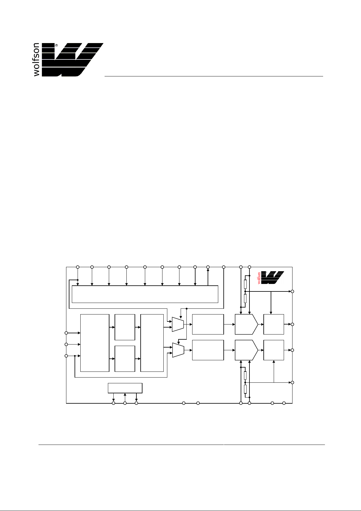
The WM8716 is a high perform ance stereo DAC designed
for audio applications such as CD, DVD, home theatre
systems, set top boxes and digital TV. The WM8716
supports data input word lengths from 16 to 24-bits and
sampling rates up to 192kHz. The WM8716 consists of a
serial interface port, di gi tal interpolation filter, multi-bit s i gma
delta modulator and stereo DAC in a small 28-pin SSOP
package. The WM8716 also inc ludes a digitally cont rollable
mute and attenuator function on each channel.
The internal digital filter has two selectable roll-off
characteristics. A sharp or slow roll-off can be selected
dependent on application requirements. Additionally, the
internal digital filter can be by-passed and the WM8716
used with an external digital filter.
The WM8716 supports two connection sc hemes for audio
DAC control. The SPI-compatible serial control port
provides access to a wide range of features inc luding onchip mute, attenuation and phase reversal. A hardware
controllable interface is also available.
BLOCK DIAGRAM
MUTEB
MODE
(24)
ML/I2S
(28)
MC/DM1
(27)
MD/DM0
(26)
DIFFHW
(17)
(25)
FEATURES
• 112dB SNR (‘A’ weighted @ 48kHz), THD: -97dB @
-1dB FS
• Sampling frequency: 8kHz to 192kHz
• Selectable digital fi l t er rol l -off
• Optional interface to indus try standard external filters
• Differential mono mode
• Input data word: 16 to 24-bit
• Hardware or SPI compatible seri al port control modes:
− Hardware mode: mute, de-emphasis, audio format
control
− Serial mode: mute, de-emphasis, attenuation (256
steps), phase reversal
• Compatible upgrade to PCM1716
APPLICATIONS
• CD, DVD audio
• Home theatre systems
• Set top boxes
• Digital TV
AGNDR
CSBIWO
(23)
RSTB
(22)
ZERO
(21)
MODE8X
(12)
(10)
AVDDR
(9)
CONTROL INTERFACE
MUTE/
BCKIN (3)
LRCIN (1)
DIN (2)
SERIAL
INTERFACE
ATTEN
MUTE/
ATTEN
CRYSTAL/OSC
(5)
(4)
XTI
CLKO
(6)
XTO
DIGITAL
FILTERS
WOLFSON MICROELECTRONICS LTD
Lutton Court, Bernard Terrace, Edi nburgh, EH8 9NX, UK
Tel: +44 (0) 131 667 9386
Fax: +44 (0) 131 667 5176
Email: [email protected]
www.wolfsonmicro.com
MUX
MUX
(15)
AVDD
SIGMA
DELTA
MODULATOR
SIGMA
DELTA
MODULATOR
(8)
DVDD
RIGHT
DAC
LEFT
DAC
(20)
AVDDL.
(19)
AGNDL
WM8716
LOW
PASS
FILTER
LOW
PASS
FILTER
(14)
AGND
(11) VMIDR
(13) VOUTR
(16) VOUTL
(18) VMIDL
(7)
DGND
Production Data Datasheets contain final
specifications current on publication date.
Supply of products conforms to Wol fson
Microelectronics’ Term s and Conditions.
2001 Wolfson Microelectronics Ltd.
Page 2
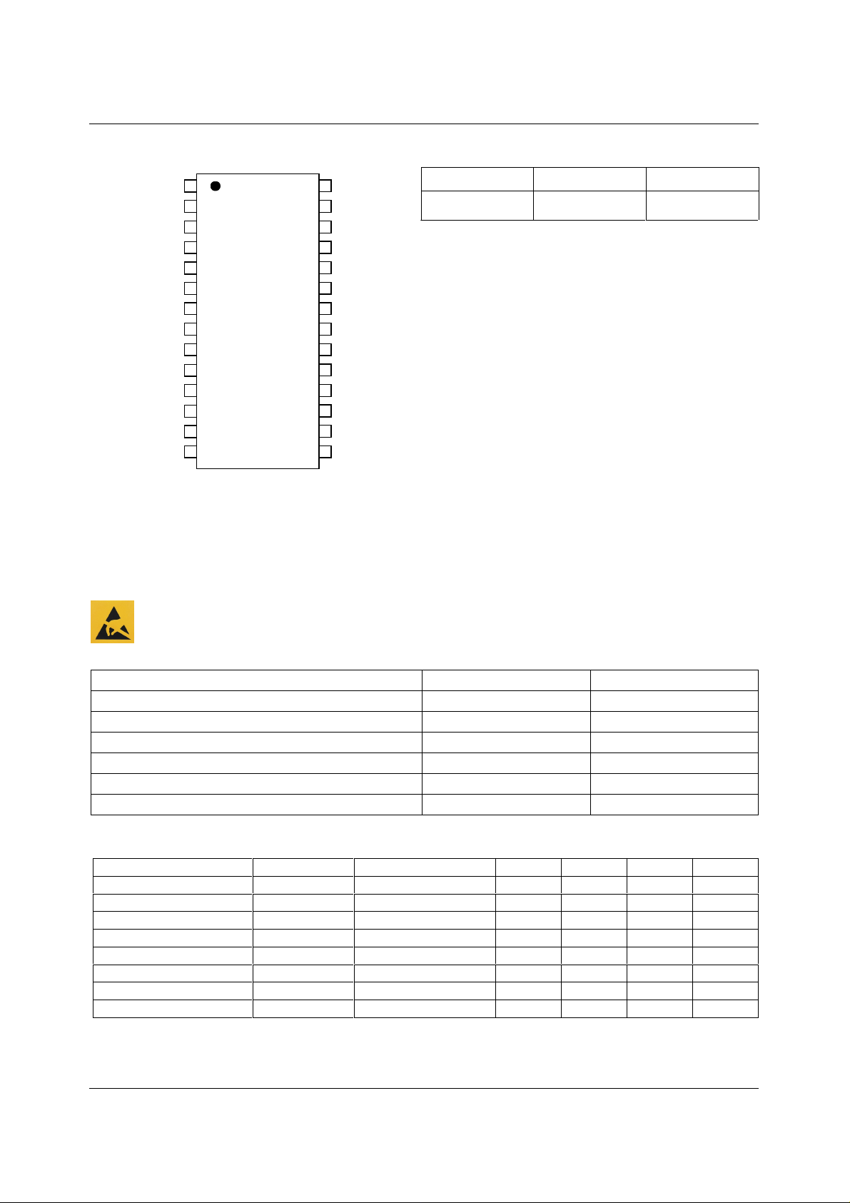
WM8716 Production Data PIN CONFIGURATION ORDERING INFORMATION
LRCIN
DIN
BCKIN
CLKO
XTI
XTO
DGND
DVDD
AVDDR
AGNDR
VMIDR
MODE8X
VOUTR
AGND
ML/I2S
1
2
3
4
5
6
7
8
9
10
11
12
13
28
MC/DM1
27
MD/DM0
26
MUTEB
25
MODE
24
CSBIWO
23
RSTB
22
ZERO
21
AVDDL
20
AGNDL
19
VMIDL
18
DIFFHW
17
VOUTL
16
AVDD
1514
DEVICE TEMP. RANGE PACKAGE
WM8716EDS -25 to +85°C 28-pin SS OP
ABSOLUTE MAXIMUM RATINGS
Absolute Maximum Ratings are s tres s rat ings only. P erm anent damage to the device may be c aused by c onti nuously operat ing at
or beyond these limits. Device functional operating lim its and guaranteed performance s pecifications are gi ven under Electrical
Characteristics at the test conditions s pecified.
ESD Sensitive Device. Thi s device i s m anufactured on a CMOS process . It i s t herefore generi cally suscept ible
to damage from excessi ve stati c voltages . Proper ES D precautions mus t be tak en during handling and st orage
of this device.
CONDITION MIN MAX
Supply voltage
Reference input
Operating temperature range, T
A
Storage temperature
Package body temperature (s ol deri ng, 10 seconds)
Package body temperature (s ol deri ng, 2 minutes)
-0.3V +7.0V
VDD + 0.3V
-25°C+85
°
C
-65°C +150°C
+240°C
+183°C
RECOMMENDED OPERATING CONDITIONS
PARAMETER SYMBOL TEST CONDITIONS MIN TYP MAX UNIT
Digital supply range
Analogue supply range
Ground
Difference DGND to AGND
Analogue supply current
Digital supply current
Analogue supply current
Digital supply current
DVDD -10% 3.3 to 5 +10% V
AVDD -10% 3.3 to 5 +10% V
AGND, DGND 0 V
-0.3 0 +0.3 V
AVDD = 5V 26 40 mA
DVDD = 5V 22 35 mA
AVDD = 3.3V 25 mA
DVDD = 3.3V 13 mA
WOLFSON MICROELECTRONICS LTD PD Rev 3.1 April 2001
2
Page 3
Production Data WM8716
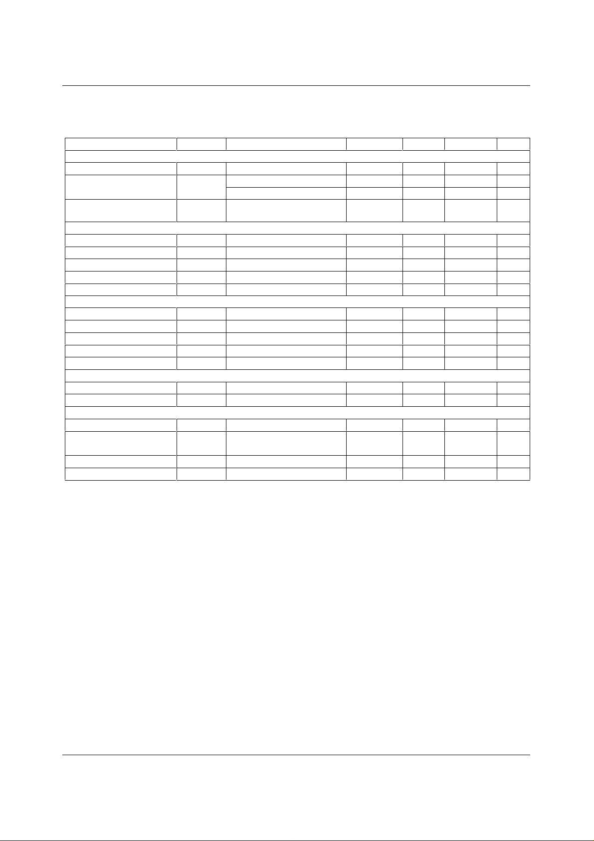
ELECTRICAL CHARACTERISTICS
TEST CONDITIONS
AVDD, DVDD = 5V, AGND, DGND = 0V , T
PARAMETER SYMBOL TEST CONDITIONS MIN TYP MAX UNIT
DAC Circuit Specifications
SNR (See Notes 1 and 2)
THD (full-scale)
(See Note 2)
Dynamic range
(See Note 2)
Filter Characteristics (Sharp Roll-off)
Passband
Stopband
Passband ripple
Stopband Attenuation
Delay time
Filter Characteristics (Slow Roll -off)
Passband
Stopband
Passband ripple
Stopband Attenuation
Delay time
Internal Analogue Filter
Bandwidth
Passband edge response
Digital Logic Levels
Input LOW level
Input HIGH level
V
V
(See Note 3)
Output LOW level
Output HIGH level
V
V
Notes:
1. Ratio of output level with 1kHz ful l scale input, to the output l evel with al l zeros into the digital input, measured ‘A’
weighted over a 20Hz to 20kHz bandwidth.
2. All performance measurem ent s done with 20kHz low pass filter. Failure to use such a filter will result in higher THD+N and
lower SNR and Dynamic Range readings than are found in the Electrical Characteri stics. The low pass fil ter removes out
of band noise; although it is not audible it may affect dynamic specifi cation values.
3. Except for Pin 12 (MODE8X) and Pin 17 (DIFFHW), where V
= +25oC, fs = 48kHz, SCKI = 256f s unless otherwise stated.
A
105 112 dB
0dB FS -92 dB
-1dB FS -97 dB
THD @ -60dB FS 105 112 dB
±0.0012 dB 0.4535fs dB
-3dB 0.491fs
f > 0.5465fs -82 dB
±0.001dB 0.274fs
-3dB 0.459fs
f > 0.732fs -82 dB
-3dB 195 kHz
20kHz -0.043 dB
IL
2.0 V
OH
IH
OL
IOL = 2mA AVSS + 0.3V V
IOH = 2mA AVDD - 0.3V
= 2.6V min.
IH
±0.0012 dB
30/fs s
±0.001 dB
9/fs s
0.8
TERMINOLOGY
1. Signal-to-noise ratio (dB) (SNR) is a measure of the difference i n l evel between the full-scale output and the output with no
signal applied.
2. Dynamic range (dB) (DNR) is a meas ure of the difference between the highest and l owest port i ons of a signal. Normally a
THD+N measurement at 60dB bel ow full scale. The measured signal i s then corrected by adding the 60dB to i t . (eg
THD+N @ -60dB= -32dB, DR= 92dB).
3. THD+N (dB) is a ratio of the r.m.s. values, of (Noise + Di stortion)/Signal.
4. Stop band attenuation (dB) is the degree t o which the frequency spectrum is attenuated (outside audio band).
5. Channel Separation (dB) (also known as Cross-Talk) is a measure of the amount one channel is isolated f rom the other.
Normally measured by sending a full-scale signal down one channel and m easuring the other.
6. Pass-Band Ripple - Any variation of the frequency response in the pass -band regi on.
WOLFSON MICROELECTRONICS LTD PD Rev 3.1 April 2001
3
Page 4
WM8716 Production Data
TEST CONDITIONS
AVDD, DVDD = 5V, AGND, DGND = 0V , T
PARAMETER SYMBOL TEST CONDITIONS MIN TYP MAX UNIT
Analogue Output Levels
Output level
Minimum resist ance load
Maximum capacitance load
Output DC level
Gain mismatc h channel to
channel
Reference Levels
Potential divider resis tance
Voltage at VMIDL/VMIDR
POR
POR threshold
= +25oC, fs = 48kHz, SCKI = 256f s unless otherwise stated.
A
Into 10kohm, full scale 0dB,
1.1
(5V supply)
Into 10kohm, full scale 0dB,
0.72 V
(3.3V supply)
To midrail or AC coupled
1 kohms
(5V supply)
To midrail or AC coupled
600 ohms
(3.3V supply)
5V or 3.3V 100 pF
AVDD/2 V
0.5 2 %FSR
AVDD to VMIDL/VMIDR and
10 kohms
VMIDL/VMIDR to AGND
AVSS/2
2.5V V
V
RMS
RMS
LRCIN
t
BCH
t
BCL
t
LB
BCKIN
t
BCY
t
BL
DIN
t
DS
t
DH
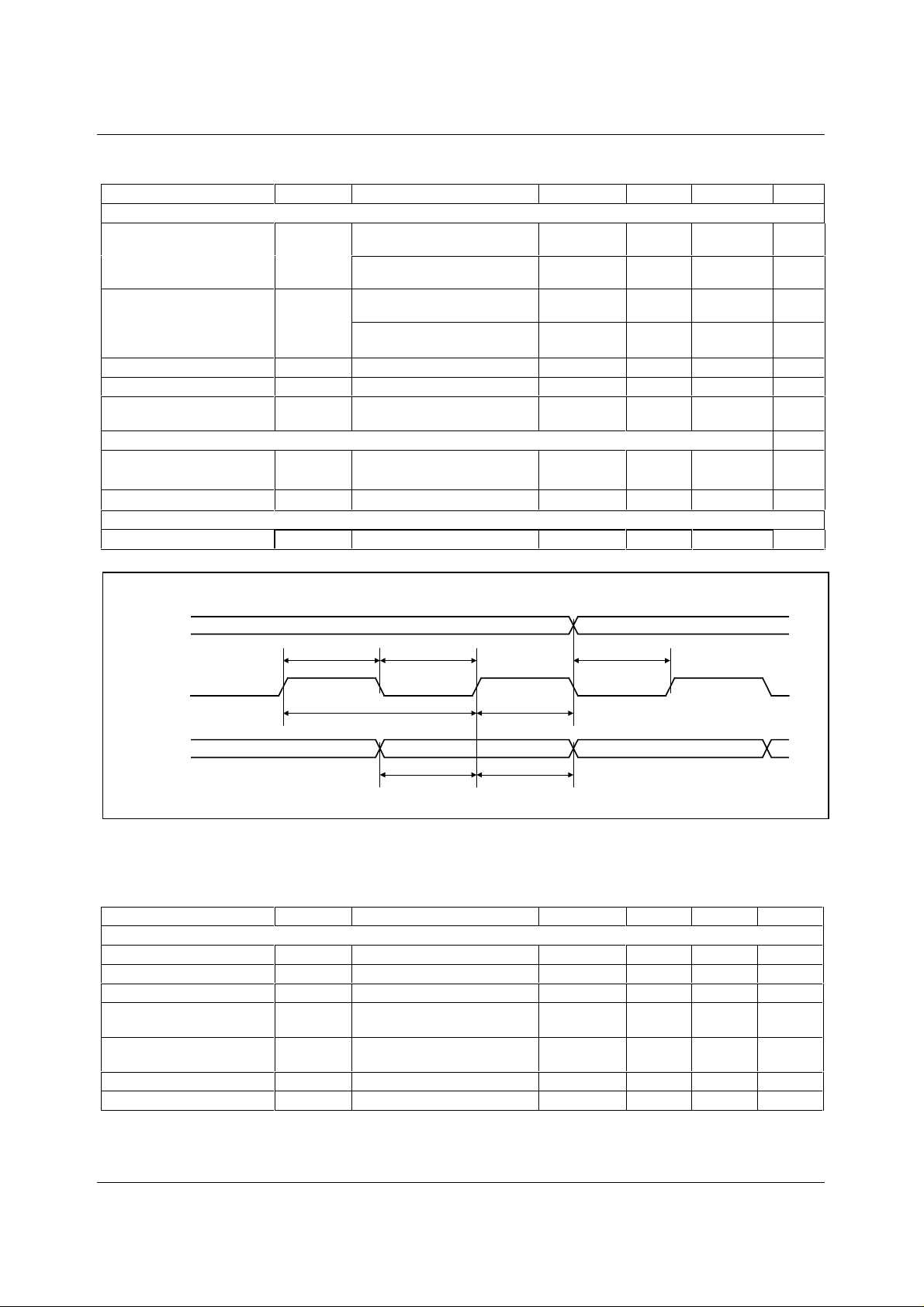
Figure 1 Audio Data Input Timing
TEST CONDITIONS
AVDD, DVDD = 5V, AGND, DGND = 0V , T
= +25oC, fs = 48kHz, SCKI = 256f s unless otherwise stated.
A
PARAMETER SYMBOL TEST CONDITIONS MIN TYP MAX UNIT
Audio Data Input Timing Information
BCKIN pulse cycle time
BCKIN pulse width high
BCKIN pulse width low
BCKIN rising edge
t
BCY
t
BCH
t
BCL
t
100 ns
50 ns
50 ns
BL
30 ns
to LRCIN edge
LRCIN rising edge
t
LB
30 ns
to BCKIN rising edge
DIN setup time
DIN hold time
t
DS
t
DH
30 ns
30 ns
WOLFSON MICROELECTRONICS LTD PD Rev 3.1 April 2001
4
Page 5
Production Data WM8716
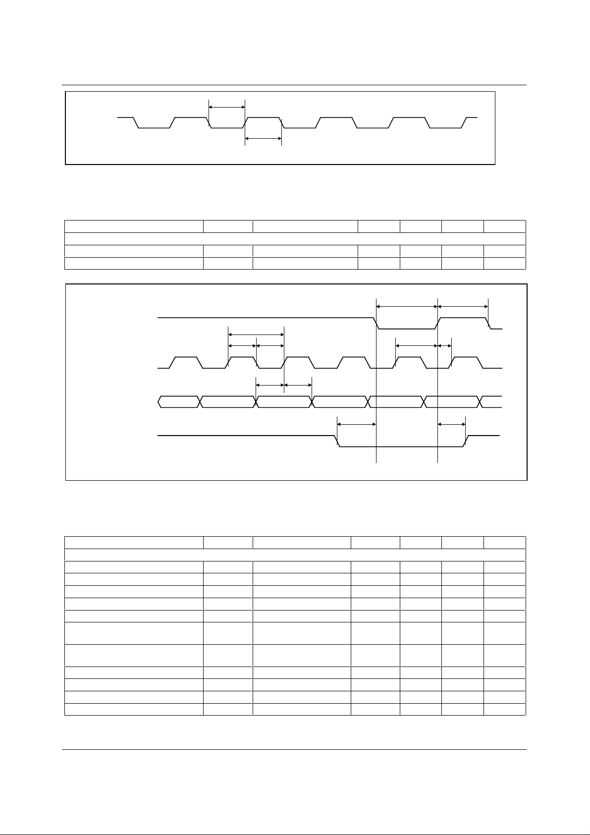
t
SCKIL
SCKI
t
SCKIH
Figure 2 System Clock Timing Requirements
TEST CONDITIONS
AVDD, DVDD = 5V, AGND, DGND = 0V , T
= +25oC, fs = 48kHz, SCKI = 256f s unless otherwise stated.
A
PARAMETER SYMBOL TEST CONDITIONS MIN TYP MAX UNIT
System Clock Timing Information
SCKI System cl ock pulse width high
SCKI System cl ock pulse width low
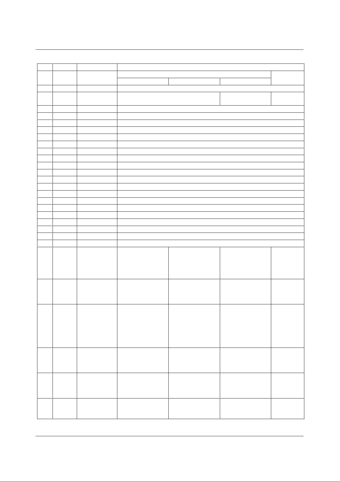
ML/I2S (PIN 28)
t
SCKIH
t
SCKIL
t
MCY
t
MCHtMCL
13 ns
13 ns
t
MLL
t
MLH
t
t
MHH
MLS
MC/DM1 (PIN 27)
t
MDStMDH
MD/DM0 (PIN 26)
t
CSML
LSB
t
MLCS
CSBIWO (PIN 23)
Figure 3 Program Register Input Timing
TEST CONDITIONS
AVDD, DVDD = 5V, AGND, DGND = 0V , T
= +25oC, fs = 48kHz, SCKI = 256f s unless otherwise stated.
A
PARAMETER SYMBOL TEST CONDITIONS MIN TYP MAX UNIT
Program Register Input Information
MC/DM1 Pulse cycle time
MC/DM1 Pulse width LOW
MC/DM1 Pulse width HIGH
MD/DM0 Hold time
MD/DM0 Set-up time
ML/I2S Low level time
(See Note 3)
ML/I2S High level time
(See Note 3)
ML/I2S Hold time
ML/I2S Set-up time
CSBIWO Low to ML/I2S low time
ML/I2S High to CSBIWO high time
t
MCY
t
MCL
t
MCH
t
MDH
t
MDS
t
MLL
t
MHH
t
MLH
t
MLS
t
CSML
t
MLCS
100 ns
40 ns
40 ns
40 ns
40 ns
40 +
1SYSCLK
40 +
1SYSCLK
40 ns
40 ns
10 ns
10 ns
Note:
3. System clock cycle.
ns
ns
WOLFSON MICROELECTRONICS LTD PD Rev 3.1 April 2001
5
Page 6
WM8716 Production Data PIN DESCRIPTION
PIN NAME TYPE DESCRIPTION
Hardware Mode
Normal Mode Differential Mode 8X Mode
1 LRCIN Digital input
2 DIN Digital input
3 BCKIN Digital input
4 CLKO Digital out put
5 XTI Analogue input
6 XTO Analogue output
7 DGND Supply
8 DVDD Supply
9 AVDDR Supply
10 AGNDR Supply
11 VMIDR Analogue output
12 MODE8X Digital input
13 VOUTR Analogue output
14 AGND Supply
15 AVDD Supply
16 VOUTL Analogue output
17 DIFFHW Digital input
18 VMIDL A nal ogue output
19 AGNDL Supply
20 AVDDL Supply
21 ZERO Digital output
22 RSTB Digital input
23 CSBIWO Digital i nput
Internal pull-down
24 MODE Digital input
Internal pull-up
25 MUTEB Digital input
Internal pull-up
26 MD/DM0 Digital input
Internal pull-up
27 MC/DM1 Digital input
Internal pull-up
28 ML/I2S Digital input
Internal pull-up
Note: Digital input pins have Schmitt trigger input buff ers except Pin 12 and Pin 17.
Sample rate clock i nput.
Audio data serial input DINL Audio data
Audio data bit clock i nput .
Oscillator buffered output (system clock).
Oscillator input.
Oscillator output.
Digital ground supply.
Digital positive supply.
Analogue positive supply.
Analogue ground supply.
Mid rail right channel.
Internal pull-down, active high, 8 x fs mode.
Right channel DAC output.
Analogue ground supply.
Analogue positive supply.
Left channel DAC output.
Internal pull-down, active high, dif ferential mono mode
Mid rail left channel.
Analogue ground supply.
Analogue positive supply.
Infinite zero detect – active low. Open drain type output with active pul l -down.
Reset input – active low. Internal pull-up.
Wordlength:
Low for 16-bit data.
High for 20-bit
(normal) or 24-bit
2
I
S data.
Low for hardware
mode.
Low to soft mute.
High for normal
operation.
Z for automute.
De-emphasis mode
select bit 0.
De-emphasis mode
select bit 1.
Audio serial format:
Low – right justified.
2
High – I
S.
Wordlength:
Low for 16-bit data.
High for 20-bit
(normal) or 24-bit
I2S data.
Low for left
mono mode.
High for right
mono mode
Low to soft mute.
High for normal
operation.
Z for automute.
Low for no
de-emphasis.
High for 44.1kHz
de-emphasis.
Low for normal filter
operation.
High for filter slow
roll-off.
Audio serial format:
Low – right justified.
High – I2S.
Wordlength:
Low for 20-bit data.
High for 24-bit data.
DINR High for
Low to soft mute.
High for normal
operation.
Z for automute.
LRP – LRCLK
polarity select.
Unused.
Leave unconnected.
Input data format:
Low – right justified.
High – left justified.
Software
Mode
serial input
Low for
serial
interface
operation.
software
mode.
Low to
soft mute.
High for
normal
operation.
Z for
automute.
Control serial
interface
data signal.
Control serial
interface
clock signal.
Control serial
interface
load signal.
WOLFSON MICROELECTRONICS LTD PD Rev 3.1 April 2001
6
Page 7

Production Data WM8716
DEVICE DESCRIPTION
The WM8716 is a high performance 128f s oversam pling rate s tereo DAC em ploying a novel 64 l evel
sigma delta DAC design which provides optimised signal-to-noise performance and clock jitter
tolerance. It is ideally suited to high quali ty audio applic ations s uch as CD, DVD-audio, hom e theat re
receivers and professional mixing consoles. The WM8716 supports sample rates from 8ks/s to
192ks/s.
The control functions of the WM8716 are either pin selec ted (hardware mode) or program med via the
serial interface (soft ware mode). Control functions that are available include: dat a input word length
and format selection (16-24 bits: I
selection (48kHz, 44.1kHz and 32kHz); differential output modes; a software or hardware mute and
independently digitally controllabl e at tenuation on both channels.
The digital filtering may be bypassed enti rely by selec ting MODE8X. Data is then input direc tly to t he
DAC, bypassing the digital filters. Left and ri ght channels are input separatel y, using the MODE pin
as the right channel input. This mode allows the use of alternative digital fil ters, such as the P acific
Microsonics PMD100 HDCD filt er.
In addition to the normal s tereo operating mode the W M8716 may also be used in dual diff erential
mode with either the left or right channel (selectable) being output dif ferentially. Two WM8716s c an
then be used in parallel to implement a stereo channel, each supporting a single channel
differentially. This mode is available in both s oftware and hardware modes and may also be us ed in
conjunction with MODE8X.
SYSTEM CLOCK
2
S, left justified or right justified): de-emphasis sample rate
Sample rates from 8ks/s up t o 96ks/s are available, and autom atically s elected, with a system cl ock
of 256fs, 384fs, 512fs or 768fs. In addition a system clock of 128fs or 192fs may be used, with
sample rates up to 192ks /s . With a 128fs or 192fs s yst em c loc k 64x oversampling mode operat ion is
automatically sel ected and the first stage of the digital filter is bypas sed.
WM8716 has an asynchronous m onitor circuit, which in t he event of removal of the mas ter system
clock, resets t he digital fi lters and analogue circ uits, m uting the out put. Re-applic ation of the sys tem
clock re-starts the filters from an intitialised state. Control registers are not reset under t hi s condition.
The WM8716 is tolerant of asynchronous bit clock jitter. The internal signal processing
resynchronises to the external LRCIN once the phase difference between bit cloc k and the system
clock exceeds half an LRCIN period. During this re-s ynch period the interpolating filters will either
miss or repeat an audio sample, minimising t he audible effects of t he operation. Table 1 shows the
typical system clock frequency inputs for the WM8716.
SAMPLING
RATE
(LRCIN)
32kHz 4.096 6.144 8.192 12.288 16.384 24.576
44.1kHz 5.6448 8.467 11.2896 16.9340 22.5792 33.8688
48kHz 6.114 9.216 12.288 18.432 24.576 36.864
96kHz 12.288 18.432 24.576 36.864 Unavailable Unavailable
192kHz 24.576 36.864 Unavailable Unavailable Unavailable Unavailable
Table 1 System Clock Frequencies Versus Sampling Rate
128fs 192fs 256fs 384fs 512fs 768fs
SYSTEM CLOCK FREQUENCY (MHZ)
WOLFSON MICROELECTRONICS LTD PD Rev 3.1 April 2001
7
Page 8
WM8716 Production Data AUDIO DATA INTERFACE
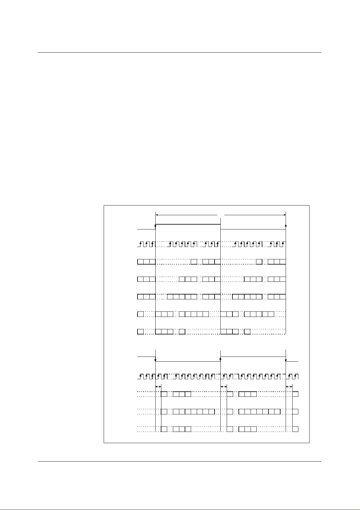
Data may be input at a rate corres ponding to the system clock having a rate of 256fs or 384fs or
512fs or 768fs, in which cas e an oversampling rat io of 128x is selec ted. Alternat ively a rate of 128fs
or 192fs may be used, in which c ase the first filter s tage is bypassed and an oversam pling ratio of
64x results. Finally, in MODE8X, data may be input at 8x the normal rate, in which case separate
input pins are used to input the t wo stereo channels of data (unless DIFFHW mode and MODE8X
are both selected, in which case only a mono channel is converted differential l y). In MODE8X all fil t er
stages are by-passed, prior to the sigma delta modul at or. Data is input MSB first in all modes.
NORMAL SAMPLE RATE
In normal mode, the dat a i s input serially on one pin for both lef t and ri ght channels.
Data can be “right justified” meaning that the last 16, 20 or 24 bits (depending on c hosen PCM word
length) that were clocked in prior t o t he transition on LRCIN are valid.
Alternatively data can be “left justified” (20 and 24-bit PCM data only), where the bit s are cloc ked in
as the first 20 or 24 bits after a transition on LRCIN.
For the three I
2
S modes supported (16-bit, 20-bit and 24-bi t P CM data), data is c loc ked “left justified”
except with one additional preceding clock cycle.
LRCIN (PIN 1)
BCKIN (PIN 3)
16-BIT RIGHT
JUSTIFIED
DIN (PIN 2)
20-BIT RIGHT
JUSTIFIED
DIN (PIN 2)
24-BIT RIGHT
JUSTIFIED
DIN (PIN 2)
24-BIT LEFT
JUSTIFIED
DIN (PIN 2)
20-BIT LEFT
JUSTIFIED
DIN (PIN 2)
LRCIN (PIN 1)
B2 B1 B0
B2 B1 B0
B2 B1 B0
B0
B0
B23 B22 B21 B20 B19
B23 B22 B21
B19 B18 B17
B15 B2 B1 B0
B19 B18 B17
B4 B3 B2 B1 B0
B0
B2 B1 B0
B2 B1 B0
1/fs
B23 B22 B21 B20 B19
B23 B22 B21
B19 B18 B17 B0
RIGHTLEFT
B15 B2 B1 B0
B19 B18 B17
B4 B3 B2 B1 B0
RIGHTLEFT
B2 B1 B0
B2 B1 B0
BCKIN (PIN 3)
2
16-BIT I
DIN (PIN 2)
24-BIT I
DIN (PIN 2)
20-BIT I
DIN (PIN 2)
S
2
S
2
S
B15
B2 B1 B0
B23
B6 B5 B4
B2 B1 B0
B19
B3 B2 B1
B0
B2 B1 B0
B15
B23
B6 B5 B4 B0
B19
B2 B1 B0
B3 B2 B1
B15
B23
B19
Figure 4 Audio Data Input Format
WOLFSON MICROELECTRONICS LTD PD Rev 3.1 April 2001
8
Page 9
Production Data WM8716
8 X FS INPUT SAMPLE RATE
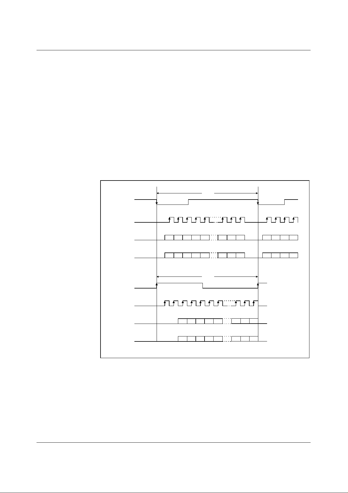
Due to the higher speed of the interface in 8 x fs mode, audio data is input on two pins. The MODE
pin (pin 24) is used as the sec ond i nput for the right channel data and left data is input on DIN (pin 2).
In this mode, software control of the device is not availabl e. The data c an be input in t wo format s, left
or right justified, s elec table by ML/I 2S and t wo word lengths (20 or 24 bi t), s elec table by CSB IWO. In
both modes the data is al ways c l ocked in MSB first.
For left justified data t he word start is marked by the falling edge of LRCIN. The data is cloc k ed i n on
the next 20/24 BCKIN rising edges. Thi s format is compatible with devices such as the PMD100.
For right justified the data i s justified to the ris ing edge of LRCIN and the data is cloc ked in on the
preceding 20/24 BCKIN rising edges before the LRCIN ris ing edge. This format is com patible with
devices such as the DF1704 or SM5842.
In both modes the polarit y of LRCIN can be switched using MD/DM0.
Differential hardware mode can be used in conjunction with 8fs mode by s etting the DIFFHW
pin high. In differential 8fs mode the data is input on DIN and output di fferentially. MODE i s unused
and must be tied low.
1/8fs
LRCIN (PIN 1)
BCKIN (PIN 3)
LEFT AUDIO
DATA DIN
(PIN 2)
RIGHT AUDIO
DATA MODE
(PIN 24)
LRCIN (PIN 1)
BCKIN (PIN 3)
LEFT AUDIO
DATA DIN
(PIN 2)
RIGHT AUDIO
DATA MODE
(PIN 24)
B19B22B23 B20B21 B2 B1 B0 B23 B22 B21 B20
B19B22B23 B20B21 B2 B1 B0 B23 B22 B21 B20
1/8fs
Figure 5 Audio Data Input Format (8 x fs Operation)
B19B22B23 B20B21 B2 B1 B0
B19B22B23 B20B21 B2 B1 B0
WOLFSON MICROELECTRONICS LTD PD Rev 3.1 April 2001
9
Page 10
WM8716 Production Data
MODES OF OPERATION
Control of the various modes of operation i s either by software control over the serial interf ace, or
by hard-wired pin control. Selection of software or hardware mode is via MODE pin. The following
functions may be controlled either via the serial control interface or by hard wiring of the
appropriate pins.
HARDWARE CONTROL MODES
When the MODE pin is held ‘low’ the following hardware modes of operation are available. In
Hardware differential mode or 8X mode some of these modes/control words are altered or
unavailable.
DE-EMPHASIS CONTROL
MDDM1
PIN 27
LLOff
L H 48kHz
H L 44.1kHz
H H 32kHz
Table 2 De-Emphasis Control
AUDIO INPUT FORMAT
CSBIIS
PIN 28
L L 16 bit normal right justified
L H 20 bit normal right justified
H L 16 bit I2S
H H 24 bit I2S
Table 3 Audio Input Format
MCDMO
PIN 26
CSBIWO
PIN 23
DE-EMPHASIS
DATA FORMAT
SOFT MUTE
Table 4 Soft Mute
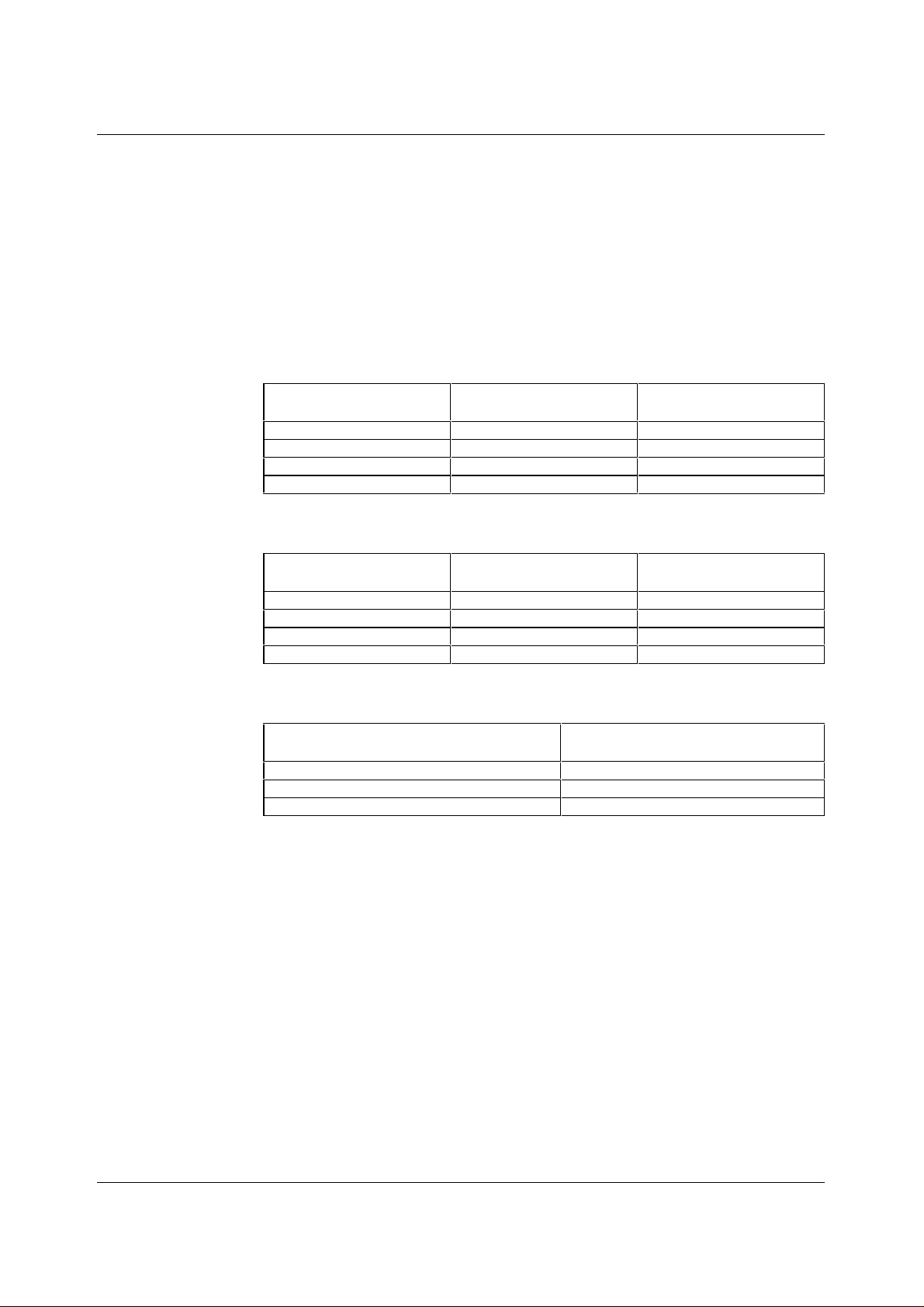
A logic low on the MUTEB pin will cause the attenuation to ramp to inf inite attenuation at a rate of
128/fs seconds per 0.5dB step. Setting MUTEB high will cause t he attenuation to ramp back to its
previous value.
Leaving MUTEB undriven allows operation of the autom ute circuit in both hardware and software
modes. On receiving 1024 cons ecut ive zero value audio s am ples , t he anal ogue s tage out put m ute is
asserted. This may be overdri ven from the MUTEB pin t o disabl e the autom ut e func tion, or out put as
a weak (10kohm) output signal.
SOFTWARE CONTROL INTERFACE
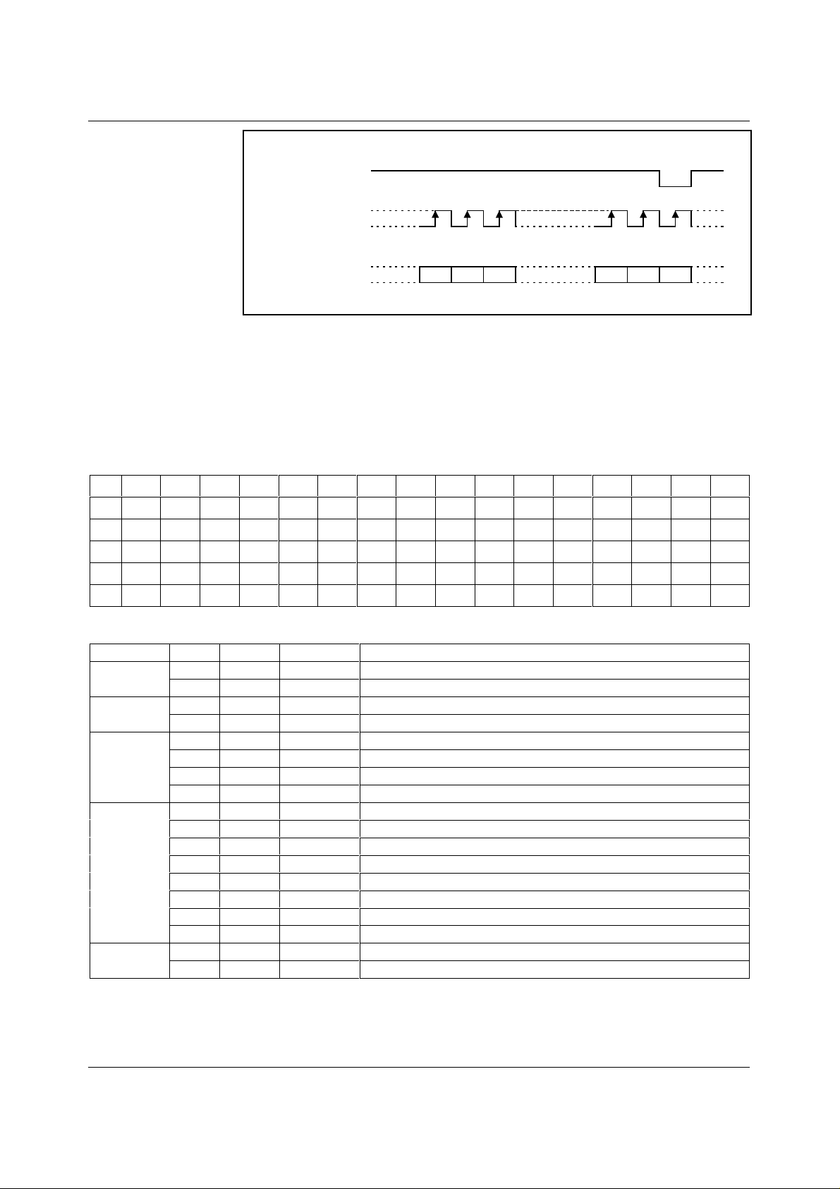
The WM8716 can be controlled using a 3-wire serial interface. MD/DM0 (pin 26) is used for the
program data, MC/DM1 (pin 22) is used to c lock in the program data and ML/I2S (pin 28) is use t o
latch in the program data. The 3-wire int erfac e protoc ol is shown in Figure 6. CS B/ IWO (pin 23) must
be low when writing.
MUTEB
PIN 25
L Mute On (no output)
Z Automute
H Mute Off (normal operation)
FUNCTION
WOLFSON MICROELECTRONICS LTD PD Rev 3.1 April 2001
10
Page 11
Production Data WM8716
ML/I2S (PIN 28)
MC/DM1 (PIN 27)
MD/DM0 (PIN 26)
Figure 6 Three-Wire Serial Interface
B15 B14 B13 B2 B1 B0
REGISTER MAP
WM8716 controls the special functions using 4 program registers, which are 16-bits long. These
registers are all loaded through input pin MD/DM0. Aft er the 16 data bits are clocked in, ML/I 2S is
used to latch in the data to the appropriate regist er. Table 5 shows the complete mapping of the
4 registers. Note that in hardware differential mode and 8X modes , software control is not available.
The hardware differential mode (Diff[1:0]) clock loss detector disable (CDD) can only be accessed by
writing to M2[8:5] with the pattern 1111. Register M4 is then accessibl e by setting A[2:0] to 110.
B15 B14 B13 B12 B11 B10 B9 B8 B7 B6 B5 B4 B3 B2 B1 B0
M0
----A2 (0)A1(0)A0(0)LDLAL7AL6AL5AL4AL3AL2AL1AL0
M1
----A2(0)A1(0)A0(1)LDRAR7AR6AR5AR4AR3AR2AR1AR0
M2
----A2(0)A1(1)A0(0)----IW1IW0OPEDEMMUT
M3
----A2(0)A1(1)A0(1)IZDSF1SF0CK0REVSR0ATCLRPI
M4
----A2(1)A1(1)A0(0)--CDDDIFF1DIFF0----
Table 5 Mapping of Program Registers
REGISTER BITS NAME DEFAULT DESCRIPTION
0
1
2
3
4
Table 6 Register Bit Descriptions
[7:0] AL[7:0] FF
8LDL 0
[7:0] AR[7:0] FF
8LDR 0
0MUT 0
1DEM 0
2OPE 0
[4:3] IW[1:0] 0
0I2S 0
1LRP 0
2ATC 0
3SR0 0
4REV 0
5CKO 0
[7:6] SF[1:0] 0
8IZD 0
[5:4] DIFF 0
6 CDD 0
Attenuation data for left channel.
Attenuation data load control for left channel.
Attenuation data for right channel.
Attenuation data load control for right channel.
Left and right DACs soft mute control.
De-emphasis control.
Left and right DACs operation c ont rol .
Input audio data bit select .
Audio data format select.
Polarity of LRCIN selec t.
Attenuator control.
Digital filter slow roll-off select.
Output phase reverse.
CLKO frequency select.
Sampling rate select.
Infinite zero detection circuit control.
Differential output mode.
Clock loss detector disable.
2
S
WOLFSON MICROELECTRONICS LTD PD Rev 3.1 April 2001
11
Page 12
WM8716 Production Data
DAC OUTPUT ATTENUATION
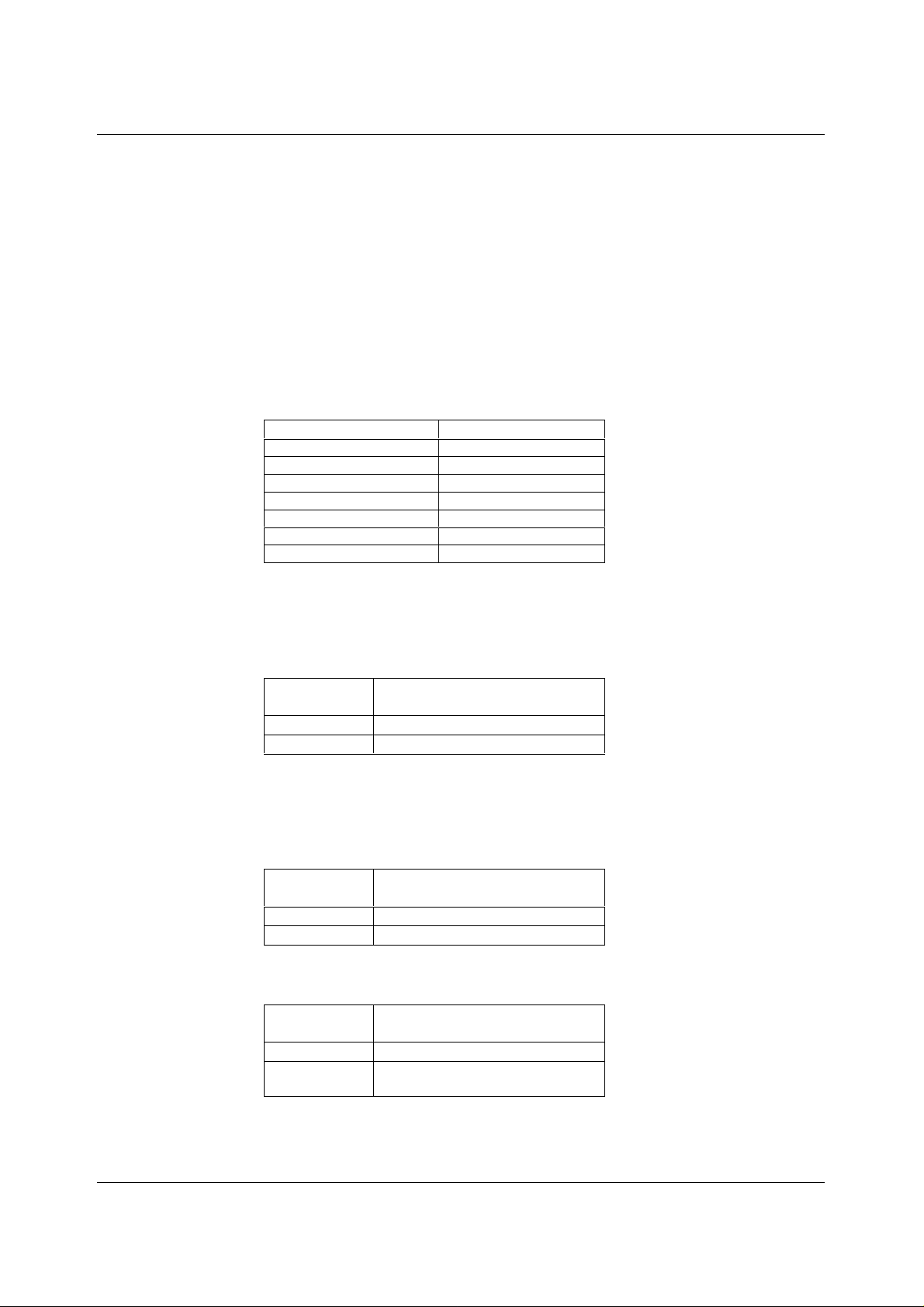
The level of attenuation for eight bi t code X, is given by:
0.5 ∗ (X - 255) dB, 1 ≤ X ≤ 255
- ∞dB (mute), X = 0
Bit 8 in register 0 (LDL) is us ed to control the l oading of attenuati on data in B [7:0]. W hen LDL is set
to 0, attenuation data will be loaded into AL[7:0], but it will not affect the filter attenuation. LDR in
register 1 has the same f unct ion f or right c hannel at tenuat ion. Onl y when LDL or LDR i s s et to ’1’ will
the filter attenuation be updated. This permits left and right channel attenuation to be updated
simultaneously.
Attenuation level is c ontrolled by AL[7:0] (left channel) or AR[7:0] (right channel). Att enuation levels
are given in Table 4.
X[7:0] ATTENUATION LEVEL
00(hex) - ∞dB (mute)
01(hex) -127.0dB
::
::
FD(hex) -1.0dB
FE(hex) -0.5dB
FF(hex) 0.0dB
Table 7 Attenuation Control Level
Bit 2 in Reg3 is used to control the attenuator (ATC). W hen ATC is “high”, the attenuation data
loaded in program register 0 is us ed for both the left and the right channels. When AT C is low, the
attenuation data for each regis t er i s applied separately to left and ri ght channels.
SOFT MUTE
MUT
(REG2, B0)
L
H
Table 8 Soft Mute
Setting MUT causes the att enuation to ramp from t he current value down to 00. The values held in
the attenuation registers are unchanged. When MUT is reset the attenuation will ramp back up to the
previous value. The ramp rate is 128/fs s/0.5dB st ep.
Soft Mute off (normal operat i on)
Soft Mute on (no output)
DIGITAL DE-EMPHASIS
DEM
(REG2, B1)
L
H
Table 9 Digital De-Emphasis
De-emphasis off
De-emphasis on
DAC OPERATION ENABLE
OPE
(REG2,B2)
L
H
Table 10 DAC Operation Enable
Normal operation
DAC output forced to bipolar zero,
irrespective of input data.
WOLFSON MICROELECTRONICS LTD PD Rev 3.1 April 2001
12
Page 13
Production Data WM8716
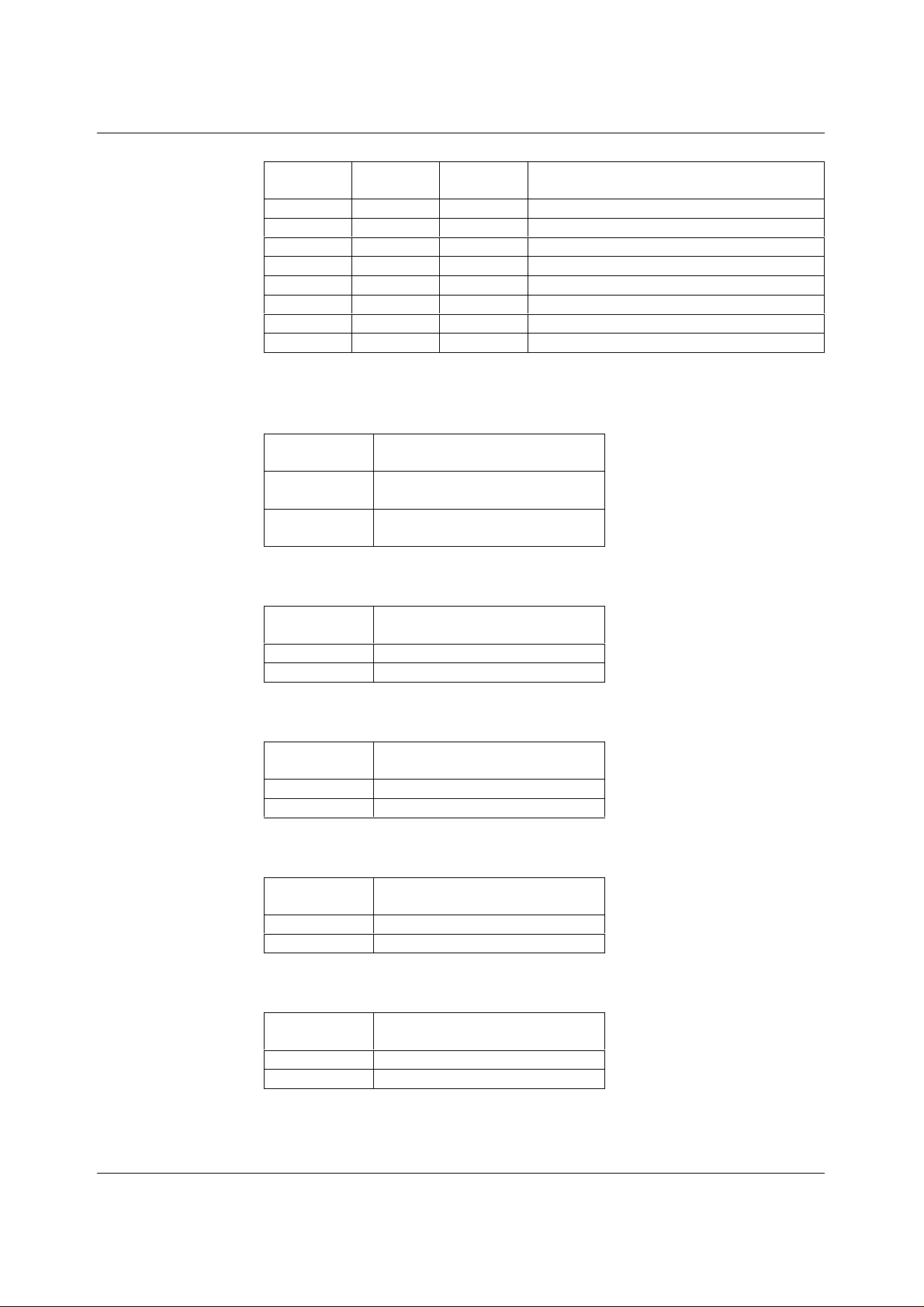
AUDIO DATA INPUT FORMAT
I2S
(REG3, B0)
000
001
010
011
100
101
110
111
Table 11 Audio Data Input Format
IW1
(REG2, B4)
IW0
(REG2, B3)
AUDIO INTERFACE
16-bit standard right justi fied
20-bit standard right justi fied
24-bit standard right justi fied
24-bit left justified (MSB first)
2
S
16-bit I
2
S
24-bit I
2
S
20-bit I
20-bit left justified (MSB first)
POLARITY OF LR INPUT CLOCK
The left channel data for a particular sample instant i s always input first, then t he ri ght channel data.
LRP
(REG3, B1)
L
H
Table 12 Polarity of LR Input Clock
LR High – left channel
LR Low – right channel
LR Low – left channel
LR High – right channel
INDIVIDUAL OR COMMON ATTENUTATION CONTROL
ATC
(REG3, B2)
L
H
Individual control
Common control from Reg0
Table 13 Individual or Common Attenuation Control
DIGITAL FILTER ROLL-OFF SELECTION
SRO
(REG3, B3)
L
H
Sharp
Slow
Table 14 Digital Filter Roll-Off Selection
ANALOGUE OUTPUT POLARITY REVERSAL
REV
(REG3, B4)
L
H
Normal
Inverted
Table 15 Analogue Output Polarity Reversal
CLKO OUTPUT FREQUENCY
CKO
(REG3, B5)
L
H
Table 16 CLKO Output Frequency
XTI
XTI/2
WOLFSON MICROELECTRONICS LTD PD Rev 3.1 April 2001
13
Page 14

WM8716 Production Data
DE-EMPHASIS SAMPLE RATE
SF1
(REG3, B7)
0 0 No de-emphasis
0 1 48kHz
1 0 44.1kHz
1 1 32kHz
Table 17 De-Emphasis Sample Rate
INFINITE ZERO DETECT
IZD
(REG3, B8)
L
H
Table 18 Infinite Zero Detect
DIFFERENTIAL MONO MODE
Using bits 4 and 5, the differential output mode m ay be selected to be one of normal stereo, reversed
stereo, mono left or mono right, as shown in Table 19.
SF0
(REG3, B6)
Zero detect mute off
Zero detect mute on
SAMPLE RATE
DIFF[1:0]
B[4:5])
00
01
10
11
Table 19 Differential Output Modes
Using these controls a pair of WM8716 devices may be used to build a ‘dual differential’ stereo
implementation with hi gher perf ormance and differential output.
DIFFERENTIAL OUTPUT MODE
Stereo
Stereo reverse.
Mono left – differential outputs.
VOUTL is left channel.
VOUTR is the negative of left channel.
Mono right – differential outputs.
VOUTL is the negative right channel.
VOUTR is right channel.
CLOCK LOSS DETECTOR DISABLE
CDD (REG4, B6)
L
R
Table 20 Clock Loss Detector Disable
When the system c loc k i s inac ti ve for approxim ately 100 µs, the cl ock los s det ect or ci rcuit detec ts the
loss of clock and the analogue circui try is forced into a mute conditi on and the digital filters reset.
Setting the CDD bit disabl es this behaviour.
Clock loss detector on
Clock loss detector off
WOLFSON MICROELECTRONICS LTD PD Rev 3.1 April 2001
14
Page 15
Production Data WM8716
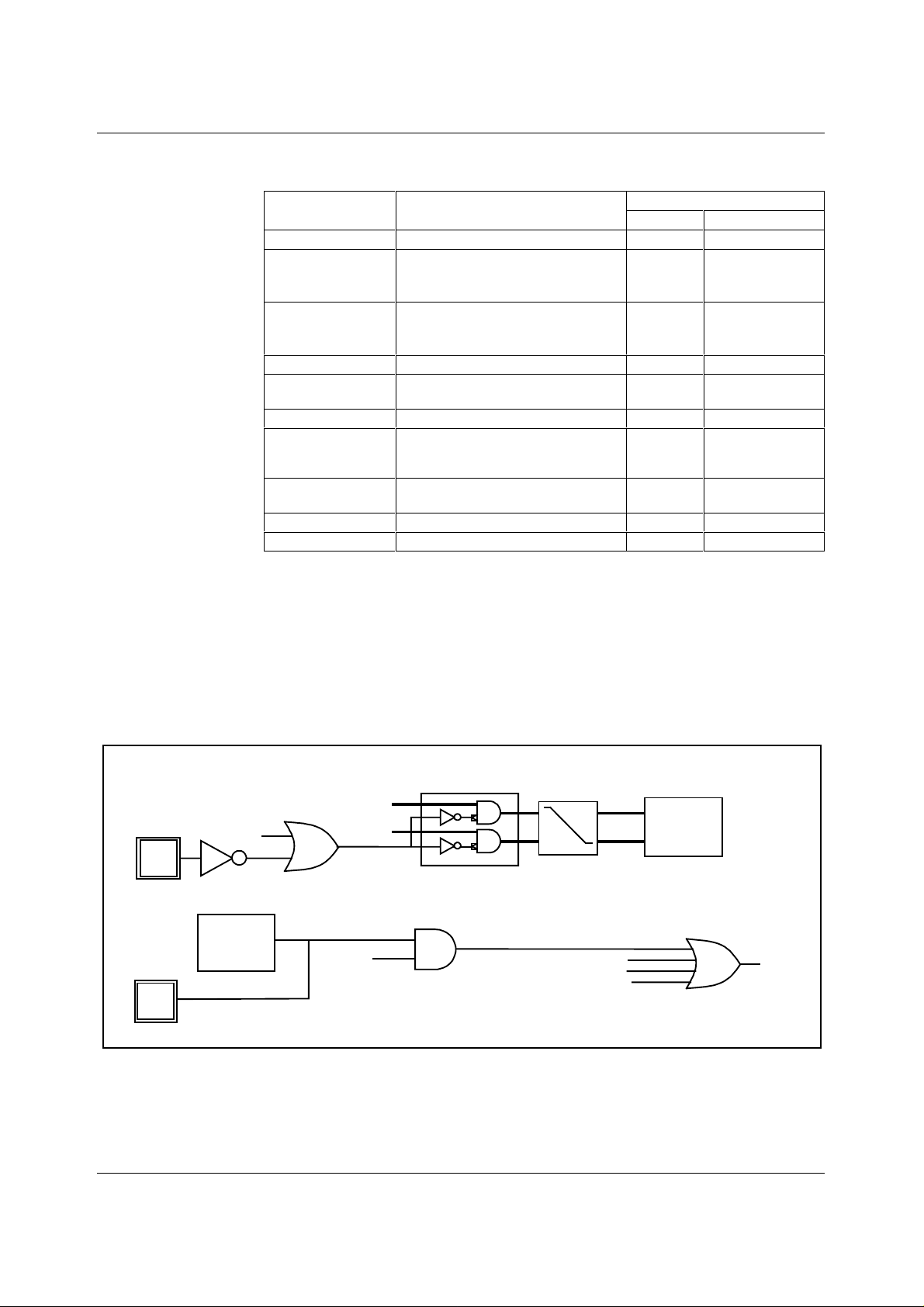
MUTE MODES
The device has various mute modes.
DIGITAL FILTER
ANALOGUE
ANRES ANMUTE
Reg bit OPE = ‘1’ Unaffected Asserted
MUTEB pin Gain ramped to zero
On release volume ramps
Asserted when
gain = 0
to previous value
AUTOMUTE
(detect 1024 zero
input samples)
Automute has no effect on digital
filters
Asserted after
1024 zero input
samples if IZD = 1
Reg bit MUT As MUTEB pin As MUTEB pin
Gain = 00
Gain = -∞dB Asserted
(left & right)
RAM initialise Gain initialised to 0dB Asserted
Loss of system
clock
Not running (no clock). On clock
restart, filters initialised, RAM
Asserted Asserted
initialised. Regist ers unchanged
No LRCLK or invalid
SCLK/LRCLK ratio
Filters initialised, RAM initialised.
Registers unchanged
Asserted Asserted
RB Reset – gain initialised to 0dB Asserted Asserted
Power-on reset Reset Asserted Asserted
Table 21 Mute Modes
• ANRE S i s the reset to the switched capacitor filter.
• ANMUTE is an anal ogue muting signal gating the analogue signal at the output (after the
SC filter)
• AUTOMUTE is asserted when both the IZD register bit i s asserted and the input audio data has
been zero on both left and right channels for 1024 input samples. The f i rst non-zero sample deasserts.
• Applyi ng a l ogi c low to MUTEB or setting MUT in Reg2 causes t he gai n regi sters to ramp to zero.
When a logic high is applied, the gain ramps sl owly back up to the value held in the appropriate
attenuation register (AL or AR). The ramp rate = 128/fs s/0.5dB step.
If SOFTMUTE is set or
MUTEB=0 then GAINL and
GAINR are overridden to 00
MUTEB
ZERO
SOFTMUTE
Automute:
Detect 1024
zero input
samples
GAINL[0:7]
GAINR[0:7]
IZD
gain ramps between
previous and new gain
setting
OPE
FREQ_INVALID
INIT
Signal
Processing
ANMUTE
Figure 7 Mute Modes
WOLFSON MICROELECTRONICS LTD PD Rev 3.1 April 2001
15
Page 16
WM8716 Production Data
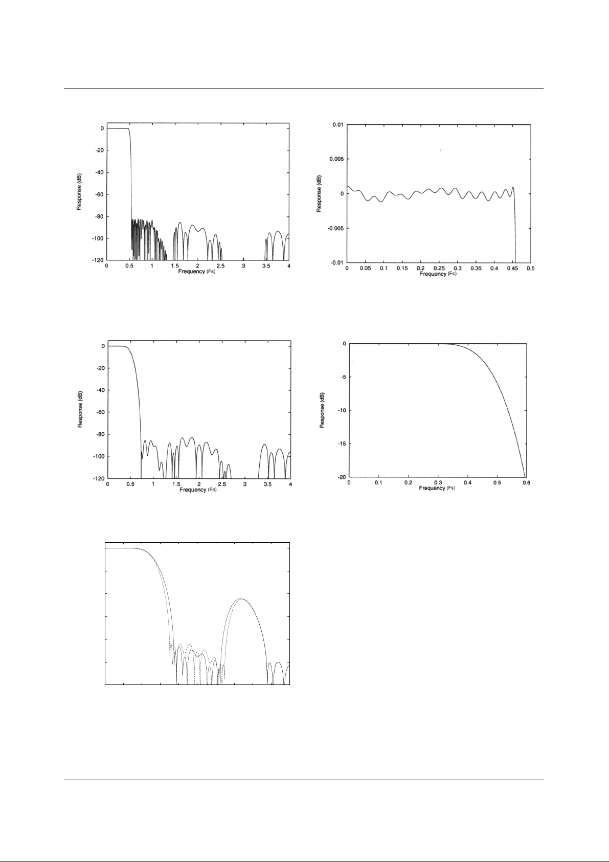
FILTER RESPONSES
Figure 8 Digital Filter Response (Sharp Roll-off Mode) Figure 9 Digital Filter Response (Sharp Roll-off Mode)
Figure 10 Digital Filter Response (Slow Roll-off Mode) Figure 11 Digital Filter Response (Slow Roll-off Mode)
0
-20
-40
-60
Response (dB)
-80
-100
-120
0 0.2 0.4 0.6 0.8 1 1.2 1.4 1.6 1.8 2
Frequency (Fs)
Figure 12 Digital Filter Response 128fs Mode (192kHz
Sample Rate) Normal Mode – Solid, Slow Mode – Dashed
WOLFSON MICROELECTRONICS LTD PD Rev 3.1 April 2001
16
Page 17

Production Data WM8716
1
0.8
0.6
0.4
0.2
0
Impulse Response
-0.2
-0.4
0 10 20 30 40 50 60
Time (input samples)
1
0.8
0.6
0.4
0.2
0
Impulse Response
-0.2
-0.4
0 10 20 30 40 50 60
Time (input samples)
Figure 13 Impulse Response (Normal Roll-off,
no De-emphasis)
Figure 14 Impulse Response (Slow Roll-off,
no De-emphasis)
WOLFSON MICROELECTRONICS LTD PD Rev 3.1 April 2001
17
Page 18
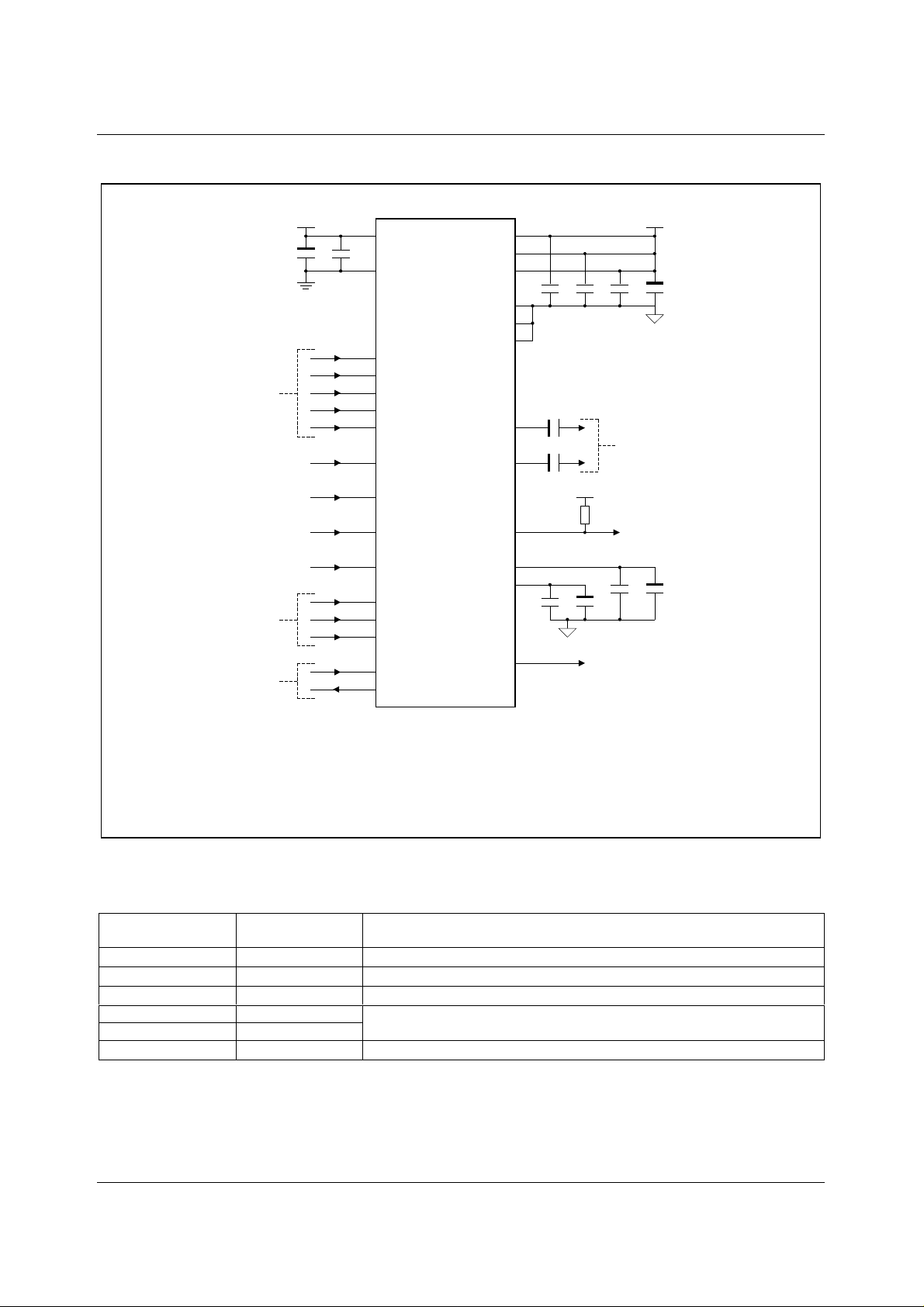
WM8716 Production Data RECOMMENDED EXTERNAL COMPONENTS
Software I/F or
Hardware Control
Audio Serial Data I/F
System Clock Input or
Oscillator Input/Output
C
DVDD
1
DGND
8
7
28
27
26
23
22
12
17
24
25
1
2
3
5
6
DVDD
DGND
ML/I2S
MC/DM1
MD/DM0
CSB/IWO
RSTB
MODE8X
DIFFHW
MODE
MUTEB
LRCIN
DIN
BCKIN
XTI
XTO
WM8716
+
C
2
AVDD
AVDDR
AVDDL
AGND
AGNDR
AGNDL
VOUTR
VOUTL
ZERO
VMIDR
VMIDL
CLKO
15
9
20
C3C4C5C
14
10
19
C
7
13
+ +
C
8
16
AVDD
R
21
11
18
C
9
4
+
C
10
AGND
XTI Buffered Output
AVDD
+
6
AGND
AC-Coupled Output
to External LPF
1
C
11
+
C
12
NOTES: 1. AGND and DGND should be connected as close to the WM8716 as possible.
2. C
to C5, C9 and C11 should be positioned as close to the WM8716 as possible.
2
3. Capacitor type used can have a big effect on device performance. It is
recommended that capacitors with very low ESR are used and that ceramics
are either NPO or COG type material to achieve best performance from the
WM8716.
Figure 15 External Components Diagram
RECOMMENDED EXTERNAL COMPONENTS VALUES
COMPONENT
REFERENCE
C1 and C6 10µF
C2 to C5 0.1µF
C7 and C8 10µF
C9 and C11 0.1µF
C10 and C12 10µF
R1 10kΩ
Table 22 External Components Description
SUGGESTED
VALUE
DESCRIPTION
De-coupling for DVDD and AVDD.
De-coupling for DVDD and AVDD.
Output AC coupling caps t o remove VMID DC level from output s.
Reference de-coupling capacit ors for VMIDR and VMIDL.
Resistor to AVDD for open drain output operation.
WOLFSON MICROELECTRONICS LTD PD Rev 3.1 April 2001
18
Page 19
Production Data WM8716
AUDIO
SERIAL
DATA
Hardware
Control
LRCIN
DIN
BCKIN
SCKI
DVDD
DVDD
DVDD
RIGHT DAC
8
7
1
2
3
5
6
4
24
25
22
28
27
26
23
DVDD
DGND
LRCIN
DIN
BCKIN
XTI
XTO
CLKO
WM8716
MODE
MUTEB
RSTB
ML/I2S
MC/DM1
MD/DM0
CSB/IWO
+
AVDD
AVDDR
AVDDL
AGND
AGNDR
AGNDL
VOUTR
VOUTL
ZERO
VMIDR
VMIDL
MODE8X
DIFFHW
15
9
20
14
10
19
13
16
21
11
18
12
17
+
-
+
AVDD
LEFT DAC
8
7
1
2
3
DVDD
DGND
LRCIN
DIN
BCKIN
+
AVDD
AVDDR
AVDDL
AGND
AGNDR
AGNDL
15
9
20
14
10
19
LPF
AVDD
+
RIGHT
OUTPUT
DATA
+
AVDD
+
5
XTI
6
XTO
4
24
25
22
28
27
26
23
CLKO
MODE
MUTEB
RSTB
ML/I2S
MC/DM1
MD/DM0
CSB/IWO
DVDD
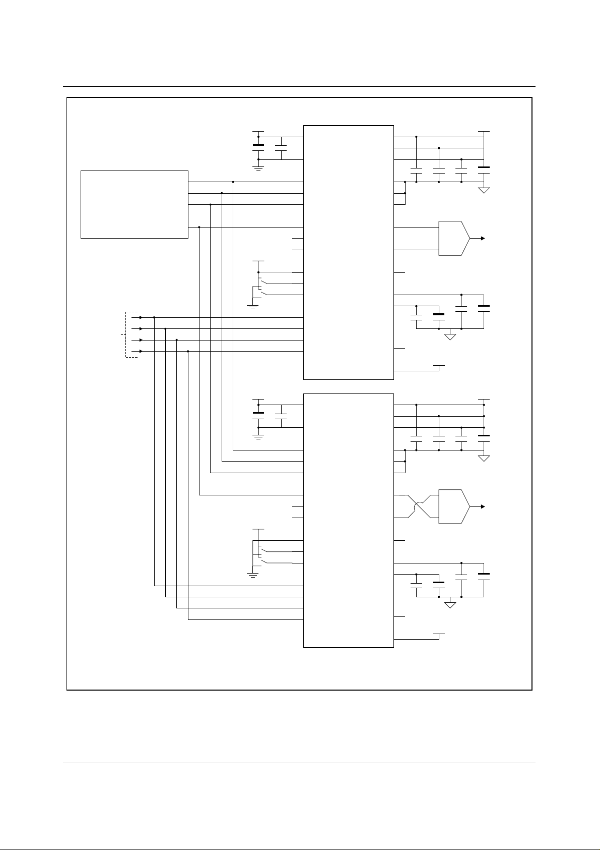
NOTE: 1. MODE selects left/right data. High for right, Low for left.
WM8716
VOUTR
VOUTL
ZERO
VMIDR
VMIDL
MODE8X
DIFFHW
13
16
21
11
18
12
17
AVDD
+
LPF
-
+
LEFT
OUTPUT
DATA
+
Figure 16 Example of 2 WM8716 S tereo DACs Configured in Hardware Differential Mode to Provide an Optimum
Performance Stereo Output
WOLFSON MICROELECTRONICS LTD PD Rev 3.1 April 2001
19
Page 20
WM8716 Production Data
SCKI
PMD-100
Serial Interface Data
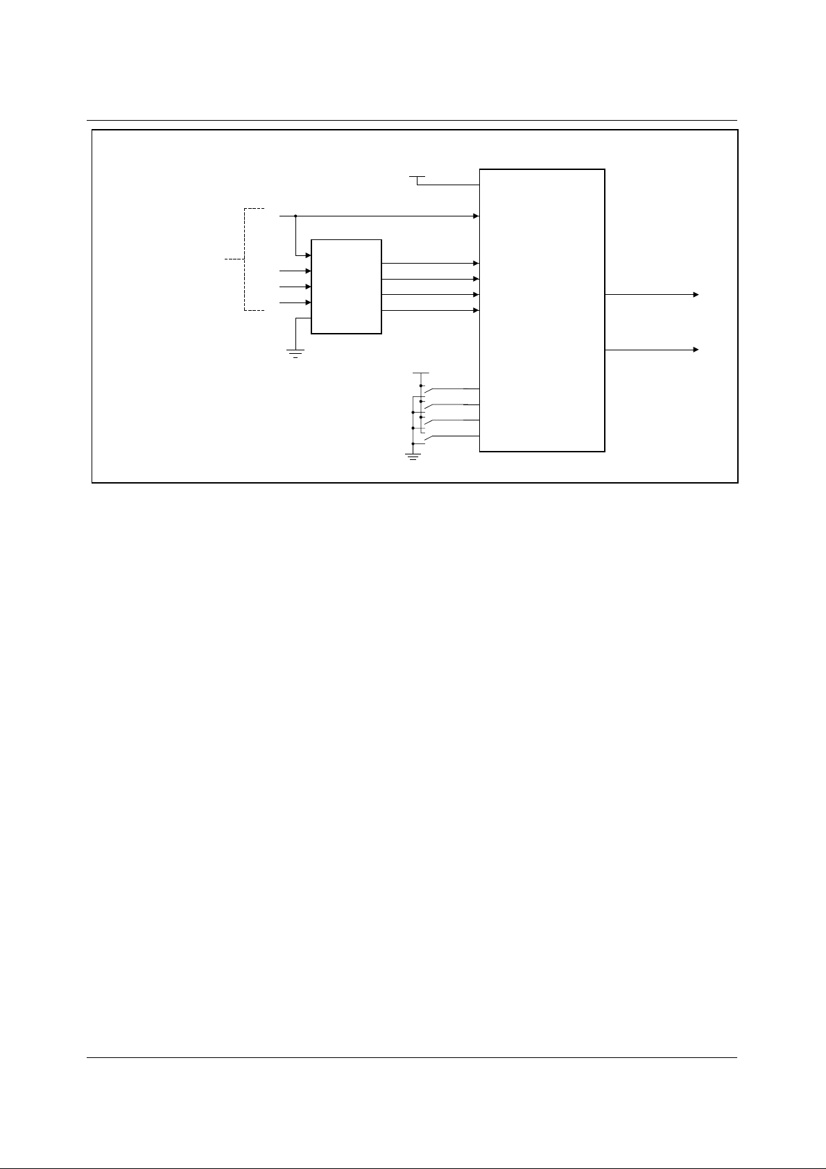
NOTES: 1. ML/I2S selects left or right justified inputs.
2. MD/DM0 selects LRCLK polarity.
3. CSBIWO selects 20 or 24-bit data.
LRCIN
BCKIN
DIN
XTI
LRCI
BCKI
DIN
PROG
(STAND ALONE
MODE)
WCKO
BCKO
DOR
Figure 17 Example of WM8716 in MODE8X Operation
DOL
+VDD
+VDD
MODE8X
XTI
LRCIN
BCKIN
DIN
MODE
WM8716
ML/I2S
CSB/IWO
MD/DM0
MUTEB
VOUTL
VOUTR
WOLFSON MICROELECTRONICS LTD PD Rev 3.1 April 2001
20
Page 21
Production Data WM8716
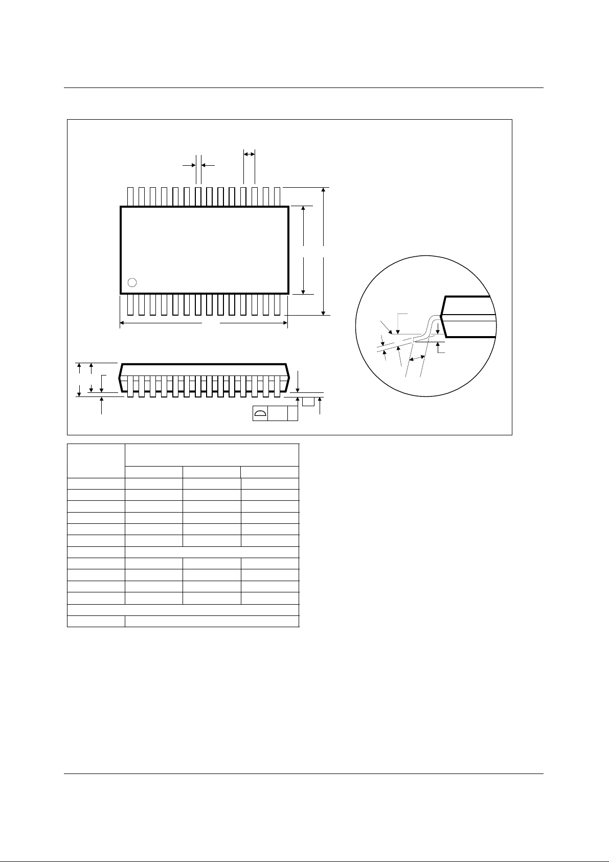
PACKAGE DIMENSIONS
DM007.CDS: 28 PIN SSOP (10.2 x 5.3 x 1.75 mm)
A1
A
A2
Symbols
A
A
1
A
2
b
c
D
e
E
E
1
L
θ
b
28
1
D
Dimensions
(mm)
MIN NOM MAX
----- ----- 2.0
0.05 ----- -----
1.62 1.75 1.85
0.22 ----- 0.38
0.09 ----- 0.25
9.90 10.20 10.50
0.65 BSC
7.40 7.80 8.20
5.00 5.30 5.60
0.55 0.75 0.95
o
0
o
4
e
15
E1 E
8
14
0.10
o
-C-
C
SEATING PLANE
GAUGE
PLANE
Θ
0.25
c
L
REF:
NOTES:
A. ALL LINEAR DIMENSIONS ARE IN MILLIMETERS.
B. THIS DRAWING IS SUBJECT TO CHANGE WITHOUT NOTICE.
C. BODY DIMENSIONS DO NOT INCLUDE MOLD FLASH OR PROTRUSION, NOT TO EXCEED 0.20MM.
D. MEETS JEDEC.95 MO-150, VARIATION = AH. REFER TO THIS SPECIFICATION FOR FURTHER DETAILS.
JEDEC.95, MO-150
WOLFSON MICROELECTRONICS LTD PD Rev 3.1 April 2001
21
 Loading...