

Page 1
WM2625
Low Power Dual 8-bit Serial Input DAC
Production Data, April 2001, Rev. 1.0
FEATURES
• Dual 8-bit voltage output DAC
• Single supply from 2.7V to 5.5V
• Low supply current
- 0.8mA typical in slow mode
- 1.8mA typical in fast mode
• DNL ±0.2 LSB, INL ±0.5 LSB (max)
• Monotonic over temperature
• DSP compatible serial interface
• Programmable settling time of 1µs or 3µs typical
• High impedance reference input buffer
APPLICATIONS
• Digital servo control loops
• I ndustri al process control
• Battery powered instruments and controls
• Machine and motion control devices
• Digital offset and gain adjustment
DESCRIPTION
The WM2625 is a dual 8-bit voltage output, resistor string
digital-to-analogue converter. It can operate with supply
voltages between 2.7V and 5.5V and can be powered down
under software control. Power down reduces current
consumption to 1µA.
The device has been designed for glueless interface t o industry
standard microprocessors and DSPs. The WM2625 is
programmed with a 16-bit serial word including 4 control bits
and 8 data bits.
Excellent performance is delivered with a typical DNL of
0.2LSBs. Monotonicity is guaranteed over the operating
temperature range. The settling time of the DAC is
programmable to allow for optimis ation of speed versus power
dissipation. The analogue output is buffered by a rail-to-rail
amplifier with a gain of two and a Class A B output stage.
The reference voltage input features a high impedance buffer
which eliminates the need to keep the reference source
ORDERING INFORMATION
DEVICE TEMP. RANGE PACKAGE
WM2625CD 0° to 70°C 8-pin SOIC
impedance low.
The WM2625 is available in an 8-pin SOIC package.
Commercial (0° to 70°C) and Industrial (-40° to 85°C)
temperature range variants are availabl e.
WM2625ID -40° to 85°C 8-pi n SOIC
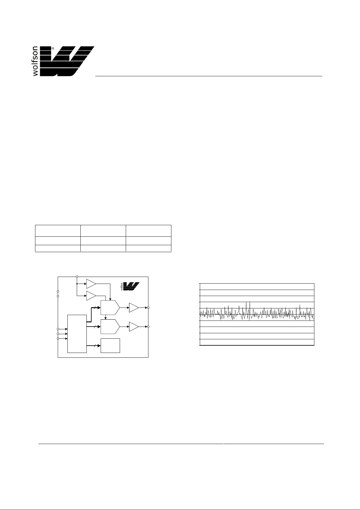
BLOCK DIAGRAM TYPICAL PERFORMANCE
REF
X1
VDD
GND
SCLK
NCS
X1
8
DAC
8
2
DAC
POWER-
DOWN AND
CONTROL
DIN
SERIAL
INTERFACE
AND
CONTROL
LOGIC
SPEED
WM2625
X2
X2
OUTA
OUTB
WOLFSON MICROELECTRONICS LTD
Lutton Court, Bernard Terrace, Edi nburgh, EH8 9NX, UK
Tel: +44 (0) 131 667 9386
Fax: +44 (0) 131 667 5176
Email: [email protected]
www.wolfsonmicro.com
0.1
VDD = 5V, V
= 2.048V, Speed = Fast Mo d e, TA = 25.5OC
0.08
0.06
0.04
0.02
-0.02
-0.04
-0.06
DNL - Differe nt ial Non-Linearity (LSBs)
-0.08
-0.1
REF
0
0 326496128160192224256
DIGITAL CODE
Production Data Datasheets contain final
specifications current on publication date.
Supply of products conforms to Wolfson
Microelectronics’ Term s and conditions.
2001 Wolfson Microelectronics Ltd.
Page 2
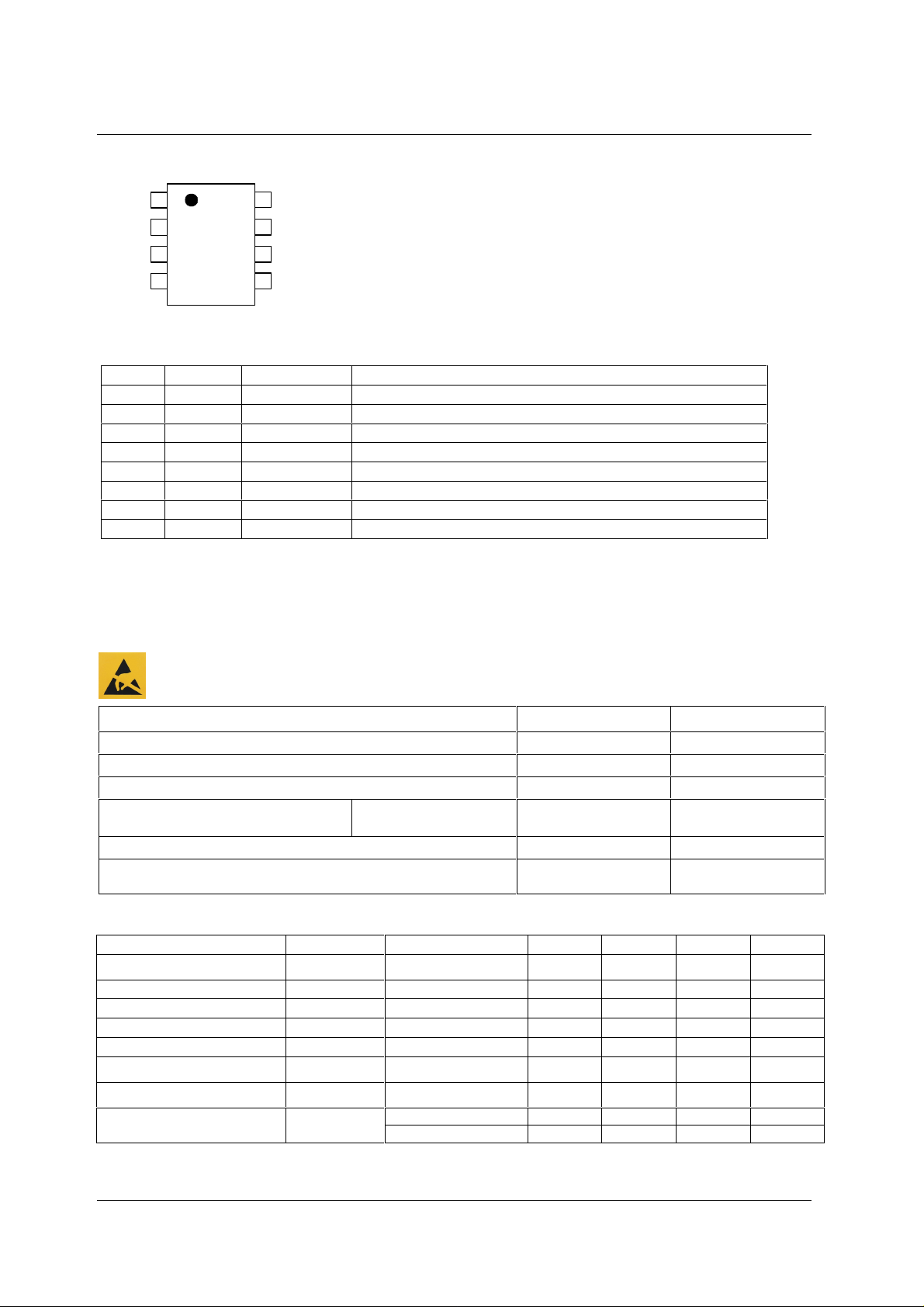
WM2625 Production Data PIN CONFIGURATION
DIN
SCLK
NCS
OUTA
1
2
3
4
VDD
8
OUTB
7
REF
6
GND
5
PIN DESCRIPTION
PIN NO NAME TYPE DESCRIPTION
1
2
3
4
5
6
7
8
DIN Digital input Serial data input
SCLK Digital input Serial cloc k input
NCS Digital input Chip select. This pin is active low.
OUTA Digit al i nput DA C A analogue voltage output
GND Supply Ground
REF Analogue input Voltage reference input
OUT Analogue output DAC B analogue vol tage output
VDD Supply Positi ve power supply
ABSOLUTE MAXIMUM RATINGS
Absolute Maximum Ratings are s tres s rat ings only. P erm anent damage to the device may be caus ed by cont inuous ly operati ng at
or beyond these limits. Device functional operating lim its and guaranteed performance s pecifications are gi ven under Electrical
Characteristics at the test conditions specified.
ESD Sensitive Device. Thi s device i s m anufactured on a CMOS process . It i s t herefore generi cally suscept ible
to damage from excessi ve stati c voltages . Proper ES D precautions mus t be tak en during handling and st orage
of this device.
CONDITION MIN MAX
Supply voltage, VDD to GND
Digital input voltage
Reference input voltage
Operating temperature range, T
A
WM2625CD
WM2625ID
Storage temperature
Soldering lead temperature, 1. 6mm (1/16 inch) from package body for
10 seconds
-0.3V VDD + 0.3V
-0.3V VDD + 0.3V
0°C
-40°C
-65°C 150°C
7V
70°C
85°C
260°C
RECOMMENDED OPERATING CONDITIONS
PARAMETER SYMBOL TEST CONDITIONS MIN TYP MAX UNIT
Supply voltage
High-level digital input voltage
Low-level digital input voltage
Reference voltage to REF pin
Load resistance
Load capacitance
Serial clock frequency
Operating free-air temperature
Note: Reference input voltages greater than VDD/2 will cause clipping for large DAC codes.
WOLFSON MICROELECTRONICS LTD PD Rev 1.0 April 2001
VDD 2.7 5.5 V
V
V
V
R
C
f
SCLK
T
IH
IL
REF
L
L
A
VDD = 2.7V to 5.5V 2 V
VDD = 2.7V to 5.5V 0.8 V
See Note
GND VDD - 1.5 V
2kΩ
100 pF
20 MHz
WM2625CD 0 70 °C
WM2625ID -40 85 °C
2
Page 3
Production Data WM2625
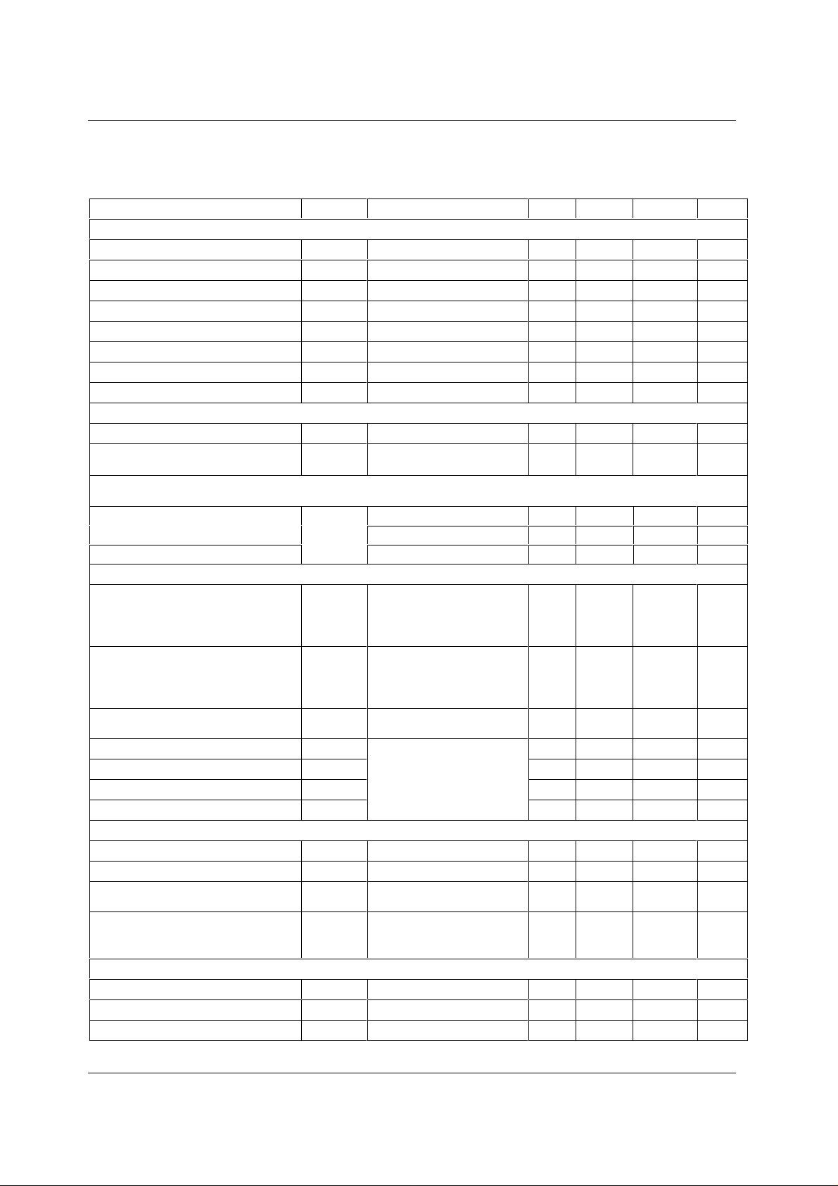
ELECTRICAL CHARACTERISTICS
Test Conditions:
R
= 10kΩ, CL = 100pF. VDD = 5V ±10%, V
L
air temperature range (unless not ed otherwise).
PARAMETER SYMBOL TEST CONDITIONS MIN TYP MAX UNIT
Static DAC Specifications
Resolution
Integral non-linearity
Differential non-linearity
Zero code error
Gain error
D.C. power supply rejection ratio
Zero code error temperature coeffi cient
Gain error temperature coefficient
DAC Output Specifications
Output voltage range
Output load regulation
Power Supplies
Active supply current
Power down supply current
Dynamic DAC Specifications
Slew rate
Full-scale settling time
Glitch energy
Signal to noise ratio
Signal to noise and distort i on rat i o
Total harmonic distort i on
Spurious free dynamic range
Reference
Reference input resistanc e
Reference input capacitanc e
Reference feedthrough
Reference input bandwidth
Digital Inputs
High level input current
Low level input current
Input capacitance
= 2.048V and VDD = 3V ±10%, V
REF
= 1.024V over recommended operati ng free-
REF
8bits
INL See Note 1 ±0.3 ±0.5 LSB
DNL See Note 2 ±0.07 ±0.2 LSB
ZCE See Note 3 ±12 mV
GE See Note 4 ±0.5 % FSR
D.C. PSRR See Note 5 -65 mV/V
See Note 6 10 ppm/°C
See Note 6 10 ppm/°C
0 VDD - 0.4 V
2kΩ to 10kΩ load
0.29 % FS
See Note 7
No load, DAC value = 128,
all digital inputs 0V or VDD
I
DD
Slow Mode 0.8 1 mA
Fast Mode 1.8 2.3 mA
See Note 8 1 3 µA
SR DAC output 10%-90%
Slow
Fast
0.5
V/µs
3
V/µs
See Note 9
t
s
DAC output 10%-90%
Slow
Fast
3
1
10
µs
3
µs
See Note 10
DIN = 0 to 1, f
= 100kHz,
CLK
5nV-s
NCS = VDD
SNR 52 54 dB
SINAD 48 49 dB
THD -50 -48 dB
SFDR
R
REFIN
C
REFIN
= 102kSPS,
f
s
f
= 1kHz,
OUT
See Note 11
V
= 1VPP at 1kHz
REF
48 50 dB
10 MΩ
5pF
-80 dB
+ 1.024V dc, DAC code 0
V
= 0.2VPP + 1.024V dc
REF
I
IH
I
IL
C
I
Slow
Fast
0.525
1.3
MHz
MHz
Input voltage = VDD -1 1 µA
Input voltage = 0V -1 1 µA
8pF
WOLFSON MICROELECTRONICS LTD PD Rev 1.0 April 2001
3
Page 4
WM2625 Production Data
Notes:
1. Integral non-linearity (INL) is the maximum deviation of the output from the line between zero and full scale (excluding t he
effects of zero code and f ul l scale errors).
2. Differential non-linearity (DNL) is the difference between the measured and ideal 1LSB am plit ude c hange of any adjac ent t wo
codes. A guarantee of monotonicity means the output voltage al ways changes in the same direc tion (or remains cons tant) as
the digital input code.
3. Zero code error is the voltage output when the DAC input code i s zero.
4. Gain error is the deviation from the ideal full-scale output excluding the effects of zero code error.
5. Power supply rejection ratio is measured by varying VDD from 4.5V to 5. 5V and measuring the proportion of this signal
imposed on the zero code error and the gain error.
6. Zero code error and Gain error temperature coefficients are norm al i sed to full-scale voltage.
7. Output load regulation is the difference between the output voltage at full scale with a 10kΩ load and 2kΩ load. It is
expressed as a percentage of the full s cale output voltage with a 10kΩ load.
8. I
is measured while continuous ly writing code 128 t o the DAC. For VIH < VDD - 0.7V and VIL > 0.7V supply current will
DD
increase.
9. Slew rate results are for the lower value of the rising and falling edge slew rates
10. Settling time is the tim e taken for the signal to settle t o within 0.5LSB of the final measured value for bot h rising and falling
edges. Limits are ens ured by design and characterisation, but are not production tested.
11. SNR, SNRD, THD and SPFDR are measured on a synthesised sine wave at frequency f
frequency f
s.
generated with a sampling
OUT
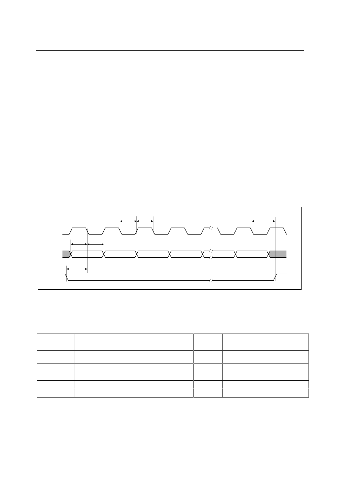
SERIAL INTERFACE
SCLK
DIN
t
WLtWH
123451516
t
SUDtHD
t
SUCSCK
D0D1D12D13D14D15
t
SUC16CS
NCS
Figure 1 Timing Diagram
Test Conditions:
R
= 10kΩ, CL = 100pF. VDD = 5V ± 10%, V
L
= 2.048V and VDD = 3V ± 10%, V
REF
= 1.024V over recommended operati ng
REF
free-air temperature range (unless noted otherwise).
SYMBOL TEST CONDITIONS MIN TYP MAX UNIT
t
SUCSCK
t
SUC16CS
t
WH
t
WL
t
SUD
t
HD
Setup time, NCS low before f i rst falling SCLK edge
Setup time, 16th falling SCLK edge (when data bit D0
is sampled) before NCS ri sing edge.
Pulse duration, SCLK high.
Pulse duration, SCLK low.
Setup time, data ready before SCLK falling edge.
Hold time, data held valid after SCLK falling edge.
10 ns
10 ns
25 ns
25 ns
10 ns
10 ns
WOLFSON MICROELECTRONICS LTD PD Rev 1.0 April 2001
4
Page 5
Production Data WM2625
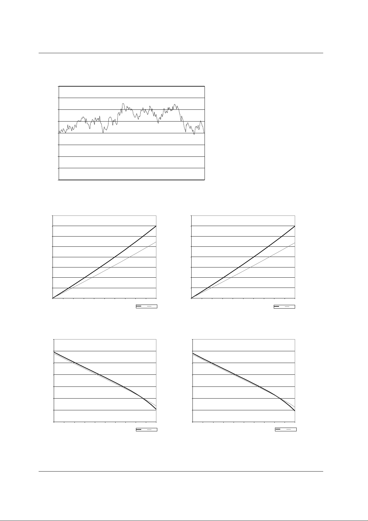
TYPICAL PERFORMANCE GRAPHS
0.2
VDD = 5V, V
= 2.048V, Speed = Fast Mode, TA = 25.5OC
0.15
0.1
0.05
0
-0.05
INL - Integral Non-Linearity (LSBs)
-0.1
-0.15
-0.2
0 32 64 96 128 160 192 224 256
Figure 2 Integral Non-Linearity
REF
DIGITAL CODE
0.4
VDD = 3V, V
0.35
0.3
0.25
0.2
0.15
OUTPUT VOLTAGE - V
0.1
0.05
0
012345678910
= 1V, Input Code = 0
REF
ISINK - mA
Slow Fast
0.4
VDD = 5V, V
0.35
0.3
0.25
0.2
0.15
OUTPUT VOLTAGE - V
0.1
0.05
0
012345678910
= 2V, Input Code = 0
REF
ISINK - mA
Figure 3 Sink Current VDD = 3V Figure 4 Sink Current VDD = 5V
OUTPUT VOLTAGE - V
2.06
2.055
2.05
2.045
2.04
2.035
VDD = 3V, V
= 1V, Input Code = 4095
REF
4.1
VDD = 5V, V
4.095
4.09
4.085
4.08
OUTPUT VOLTAGE - V
4.075
= 2V, Input Code = 4095
REF
Slow Fast
2.03
2.025
012345678910
ISOURCE - mA
Slow Fast
4.07
4.065
012345678910
ISOURCE - mA
Slow Fast
Figure 5 Source Current VDD = 3V Figure 6 Source Current VDD = 5V
WOLFSON MICROELECTRONICS LTD PD Rev 1.0 April 2001
5
Page 6
WM2625 Production Data DEVICE DESCRIPTION
GENERAL FUNCTION
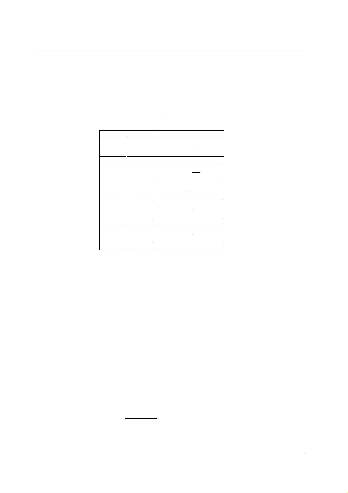
The WM2625 is a dual 8-bit, voltage output DAC operating from a single s upply. It uses a res istor
string network buffered with an op amp to convert 8-bit digi tal data to analogue vol tage levels (see
Block Diagram). The out put voltage is determined by the referenc e i nput voltage and the input code
according to the following relationship:
2
V
out
INPUT OUTPUT
1111 1111
::
1000 0001
1000 0000
0111 1111
::
0000 0001
0000 0000 0V
Table 1 Binary Code Table (0V to 2V
CODE
V
()
REFIN=
256
2
255
2
()
REFV
256
129
2
()
REFV
256
128
()
256
127
2
()
REFV
256
2
()
REFV
256
Output), Gain = 2
REF
REFREF VV =
1
POWER ON RESET
An internal power-on-reset circuit resets the DAC register to all 0s on power-up.
SERIAL INTERFACE
BUFFER AMPLIFIER
The output buffer has a near rail-to-rail output with s hort circuit protect ion and can reliably drive a
2kΩ load with a 100pF load capacitance.
EXTERNAL REFERENCE
The reference voltage input is buffered which makes the DAC input resistance independent of
code. The REF pin has an input resis tanc e of 10MΩ and an input capacitance of typic ally 5pF. The
reference voltage determines the DAC full-scale output.
Before writing any data to the WM2625, the interface must be enabled by setting NCS to low.
Incoming data on DIN (st arting with the MSB) is then shift ed bit-per-bit int o the int ernal regist er on
the falling edges of SCLK. From there data is loaded into t he target latch aft er 16 bits have been
transferred, or when NCS rises. Three int ernal latches can be addressed: DAC A, DAC B, or t he
buffer latch. This makes it possible to update both DACs simultaneously or to update one
independently of the other (see ‘Addressing the Buffer and DAC Latches ’, below).
SERIAL CLOCK AND UPDATE RATE
Figure 1 shows the device timing. The maximum serial rate is :
f
SCLK
max
=
1
tt
+
WLWH
minmin
MHz
20
=
WOLFSON MICROELECTRONICS LTD PD Rev 1.0 April 2001
6
Page 7
Production Data WM2625
Since a data word contains 16 bits , the sample rate for one channel is l i mited to
f
=
s
max
16
For full two-channel operation, where two data words need to be transmitted per sam pl e, thi s f igure
is halved to 625kHz. However, the DAC settli ng time to 8-bit acc uracy limits the response time of
the analogue output for large input st ep transitions.
1
()
tt
+×
WLWH
minmin
SOFTWARE CONFIGURATION OPTIONS
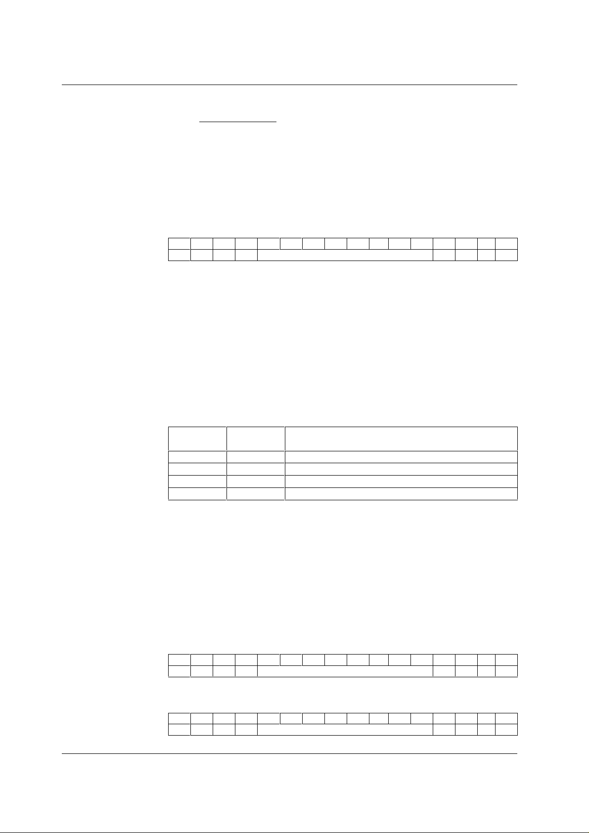
Table 2 shows the composition of a 16-bit data word. D11-D4 contains the 8-bit data word, and
D14-D13 hold the programmable options . Bits D15 and D12 are used for addres sing the diff erent
latches. D3 to D0 are unused and shoul d be set to ZERO.
D15 D14 D13 D12 D11 D10 D9 D8 D7 D6 D5 D4 D3 D2 D1 D0
R1 SPD PWR R0 New DAC value (8 bits) 0 0 0 0
Table 2 Register Map
PROGRAMMABLE CONVERTER SPEED
SPD (Bit 14) allows for software control of the converter s peed. A ONE selects the fast mode,
where typical settling tim e to within ±0.5LSB of the final value i s 1µs. a ZERO puts the device into
the slow mode, where typical settl i ng time is 3µs.
PROGRAMMABLE POWER DOWN
The power down function is controlled by PWR (Bit 13). A ZERO configures the devi ce as active,
or fully powered up, a ONE sets the device into power down mode. When the power down function
is released the device reverts to the DAC code set prior to power down.
ADDRESSING THE BUFFER AND DAC LATCHES
Data received on the serial interface is routed according t o the values of bits R1 and R0, as shown
in Table 3
MHz
25.1
=
R1
(BIT D15)
00
01
10
11
Table 3 Latch Addressing
To update both DACs simul taneously, the data intended for DAC B should first be s tored in the
buffer. Subsequently, writing data to DAC A will automatically update the DAC B latch from the
buffer, so that the analogue output of both DACs will change at the same time.
When updating the two channels independently, all data written to the DAC B l atch (R1 and R0 s et
to ZERO) is also copied to t he buffer. Thus the autom atic update of DAC B when writing to DAC A
latch (R1=1, R0=0) does not change the DAC B data. Data should not be written only to t he buffer
when operating in this mode.
R0
(BIT D12)
REGISTER
Write data to DAC B and buffer
Write data to buf fer
Write data to DAC A and update DAC B with buffer content
Reserved
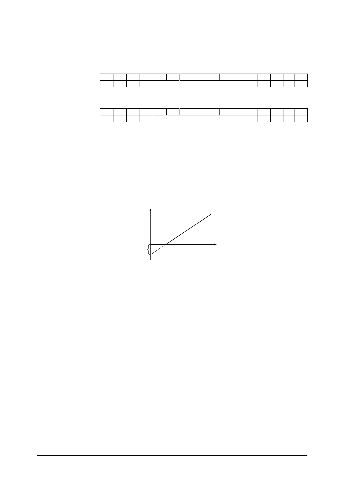
EXAMPLES OF OPERATION
Simultaneous operation, slow mode:
1. Write data for DAC B to buffer
D15 D14 D13 D12 D11 D10 D9 D8 D7 D6 D5 D4 D3 D2 D1 D0
0 0 0 1 New DAC B value 0 0 0 0
2. Write new DAC A value and update DAC B from buffer simultaneously
D15 D14 D13 D12 D11 D10 D9 D8 D7 D6 D5 D4 D3 D2 D1 D0
1 0 0 0 New DAC A value 0 0 0 0
WOLFSON MICROELECTRONICS LTD PD Rev 1.0 April 2001
7
Page 8
WM2625 Production Data
Independent operation, fast mode:
Set DAC B output (fast mode):
D15 D14 D13 D12 D11 D10 D9 D8 D7 D6 D5 D4 D3 D2 D1 D0
0 1 0 0 New DAC B value 0 0 0 0
Set DAC A output (fast mode):
D15 D14 D13 D12 D11 D10 D9 D8 D7 D6 D5 D4 D3 D2 D1 D0
1 1 0 0 New DAC A value 0 0 0 0
APPLICATIONS INFORMATION
LINEARITY, OFFSET, AND GAIN ERROR
Amplifiers operating from a single supply can have positive or negative voltage offsets. With a
positive offset, t he output voltage changes on the first code transition. However, if the offset is
negative, the output voltage may not change with the firs t c ode, depending on t he m agnit ude of t he
offset voltage. This is because with t he most negative supply rail being ground, any attempt to
drive the output amplifier below ground will clamp the output at 0 V. The output voltage then
remains at zero until the input code is suf ficiently high to overcome the negative offset voltage,
resulting in the transfer f unction shown in Figure 7.
Output
Voltage
0 V
Negative
Offset
Figure 7 Effect of Negative Offset
This offset error, not t he linearity error, produces t he breakpoint. The t ransfer funct ion would fol low
the dotted line if the output buf fer could drive below the ground rail.
DAC linearity is measured between zero-input code (all input bits at 0) and full-scale code (all
inputs at 1), disregarding off set and ful l-sc ale errors . However, due to the break point in t he t ransf er
function, single supply operati on does not all ow for adjustm ent when the offs et is negat ive. In s uch
cases, the linearity is theref ore measured between full-scal e and the lowest code that produces a
positive (non-zero) output voltage.
DAC code
POWER SUPPLY DECOUPLING AND GROUNDING
Printed circuit boards with s eparate analogue and digital ground planes deliver the best s ystem
performance. The two ground planes should be connected together at the low im pedance power
supply source. Ground currents should be managed so as to minim ise voltage drops across the
ground planes.
A 0.1µF decoupling capacitor should be connected between the posit ive supply and ground pins of
the DAC, with short leads as c lose as possible to the device. Use of ferrite beads may further
isolate the system analogue supply from the digit al supply.
WOLFSON MICROELECTRONICS LTD PD Rev 1.0 April 2001
8
Page 9
Production Data WM2625
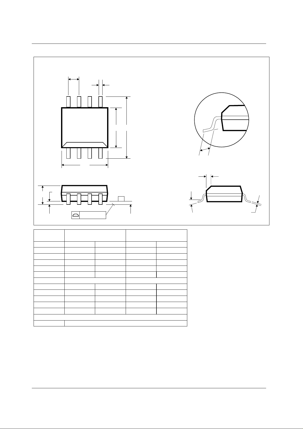
PACKAGE DIMENSIONS
D: 8 PIN SOIC 3.9mm Wide Body
e
D
A1
A
B
58
41
E H
-C-
h x 45
α
DM009.B
L
o
Symbols
0.10 (0.004)
Dimensions
(mm)
SEATING PLANE
Dimensions
(Inches)
MINMAXMINMAX
A
A
1
B
C
D
e
E
h
H
L
α
1.35 1.75 0.0532 0.0688
0.10 0.25 0.0040 0.0098
0.33 0.51 0.0130 0.0200
0.19 0.25 0.0075 0.0098
4.80 5.00 0.1890 0.1968
1.27 BSC 0.050 BSC
3.80 4.00 0.1497 0.1574
0.25 0.50 0.0099 0.0196
5.80 6.20 0.2284 0.2440
0.40 1.27 0.0160 0.0500
o
0
o
8
o
0
o
8
REF: JEDEC.95, MS-012
NOTES:
A. ALL LINEAR DIMENSIONS ARE IN MILLIMETERS (INCHES).
B. THIS DRAWING IS SUBJECT TO CHANGE WITHOUT NOTICE.
C. BODY DIMENSIONS DO NOT INCLUDE MOLD FLASH OR PROTRUSION, NOT TO EXCEED 0.25MM (0.010IN).
D. MEETS JEDEC.95 MS-012, VARIATION = AA. REFER TO THIS SPECIFICATION FOR FURTHER DETAILS.
C
WOLFSON MICROELECTRONICS LTD PD Rev 1.0 April 2001
9
 Loading...