

Page 1
WM2148
14-bit 8MSPS Analogue-To-Digital Converter
Production Data, February 2001, Rev 1.1
DESCRIPTION
The WM2148 is a 14-bit, 8 MSPS analogue to digital
converter with an on-chip voltage reference, high bandwidth
sample and hold amplifier and programmable gain. The
analogue input is differential, giving excellent commonmode noise imm uni ty and low distortion.
The WM2148 is designed for us e in highly integrated, lowpower 3.3V systems. A high speed, microprocessor
compatible parallel int erface all ows control of the ADC input
gain, digital DC offset, internal / external reference and
output data format. Both binary and two’s complement
formats are supported. The devi ce also features an out of
range indicator pin to show when the input si gnal exceeds
the converter’s full-s cale range.
In Power Down mode, all analogue circuitry is internally
disconnected from t he power supply, reducing total supply
current to 20µA.
The WM2148 is available in a 1mm thin 48-pin TQFP
package in standard comm ercial and industrial temperature
ranges.
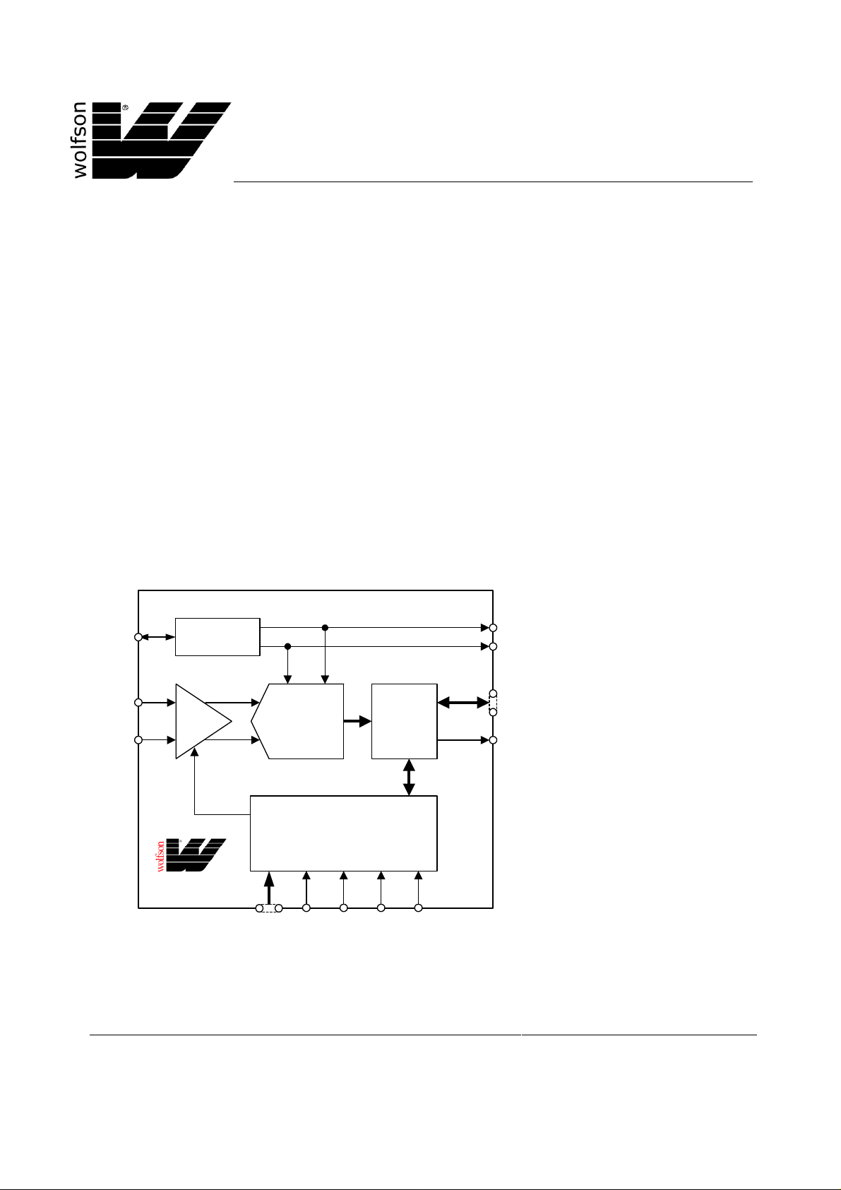
BLOCK DIAGRAM
FEATURES
• 14-bit resolution ADC
• 8 MSPS conversion rate
• Differential input
• 3.3V single supply
• Very low current power down mode - 20µA typical
• Microprocessor compat i ble parallel interface
• Internal or external voltage reference
• High bandwidth sample and hold ampli f ier
- 140MHz full-power bandwidth
• Programmable Gain Amplifier (PGA)
• Programmable DC offset
• Binary or two’s complement output format
• Out of range indicator
• 48-pin TQFP package, body thickness 1mm
APPLICATIONS
• Communications
• xDSL Front ends
• Industrial control
• Instrumentation
VBG
IN+
IN-
PRECISION
REFERENCE
+
PGA
-
WM2148
ADC
PARALLEL INTERFACE AND
CONTROL LOGIC
A[1:0] CSB WEB OEB
BUFFERS
REF+
REF-
D[13:0]
OUTPUT
OVI
CLK
WOLFSON MICROELECTRONICS LTD
Bernard Terrace, Edinburgh, EH8 9NX, UK
Tel: +44 (0) 131 667 9386
Fax: +44 (0) 131 667 5176
Email: [email protected]
http://www.wolfson.co.uk
Production Data datasheets contain final
specifications current on publication date.
Supply of products conforms to W ol fson
Microelectronics’ Term s and Conditions.
2001 Wolfson Microelectronics Ltd.
Page 2
WM2148 Production Data
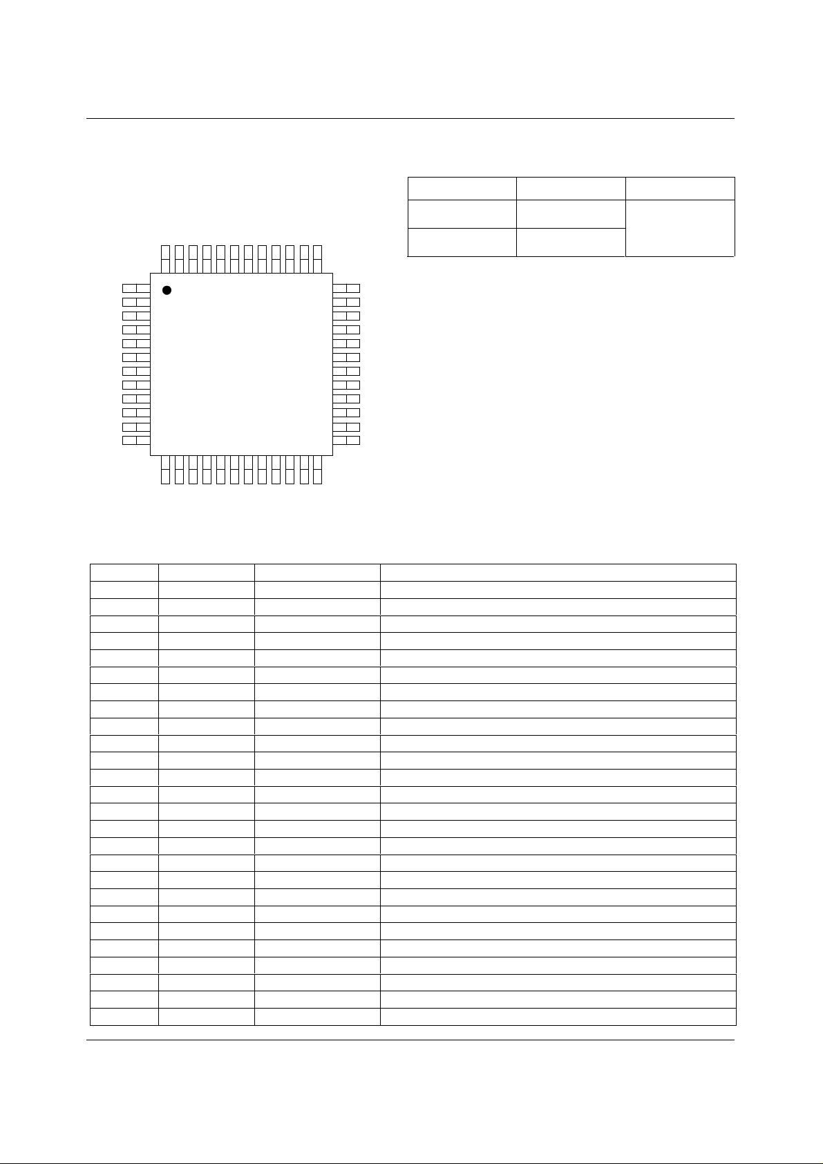
PIN CONFIGURATION ORDERING INFORMATION
DEVICE TEMP. RANGE PACKAGE
2
D
D
N
D
+
V
G
N
A
I
A
C
1
B
D
D
D
U
N
S
D
D
G
V
A
A
0
V
V
A
1
A
D
A
B
C
S
C
N
C
N
L
R
T
1
2
WM2148CFT/V 0 to +70oC
WM2148IFT/V
-40 to +85
o
C
1 mm thick body
48-pin TQFP
AVDDREF
VBG
CML
REF+
REF-
AGNDREF
VSUB
DGNDLOGIC
48 38394041424344454647 37
IN-
OVI
D13
D12
1
2
3
4
5
6
7
8
9
10
11
12
14 21201918171615 24232213
D8
DGNDOP1
D9
D10
D11
DVDDOP1
D6
D7
DVDDOP3
D5D3D4
36
35
34
33
32
31
30
29
28
27
26
25
WRB
OEB
DGNDCTRL
DGNDCLK
CLK
DVDDCLK
DVDDLOGIC
D0
D1
D2
DVDDOP2
DGNDOP2
PIN DESCRIPTION
PIN NAME TYPE DESCRIPTION
1 IN- Analogue Input
2 AVDDREF Supply
3 VBG Analogue I/O
4 CML Analogue Output
5 REF+ Analogue Output
6 REF- Analogue Output
7 AGNDREF Supply
8 VSUB Supply
9 DGNDLOGIC Supply
10 OVI Digital Output
11 D13 Digital I/O
12 D12 Digital I/O
13 D11 Digital I/O
14 DVDDOP1 Supply
15 DGNDOP1 Supply
16 D10 Digital I/O
17 D9 Digital I/O
18 D8 Digital I/O
19 D7 Digital I/O
20 DVDDOP3 Supply
21 D6 Digital I/O
22 D5 Digital I/O
23 D4 Digital I/O
24 D3 Digital I/O
25 DGNDOP2 Supply
26 DVDDOP2 Supply
Negative Differential Analogue I nput
Positive Supply Volt age for Reference
Bandgap Voltage / External Reference
Reference Decoupling Point
Positive Reference Voltage
Negative Reference Voltage
Reference Block Ground
Device Substrate
Digital Ground for Logic Block
Out of Range Indicator
Data Bit 13
Data Bit 12
Data Bit 11
Positive Supply for Output Drivers
Ground for Output Drivers
Data Bit 10
Data Bit 9
Data Bit 8
Data Bit 7
Positive Supply for Output Drivers
Data Bit 6
Data Bit 5
Data Bit 4
Data Bit 3
Ground for Output Drivers
Positive Supply for Output Drivers
WOLFSON MICROELECTRONICS LTD PD Rev 1.1 February 2001
2
Page 3

Production Data WM2148
PIN NAME TYPE DESCRIPTION
27 D2 Digital I/O
28 D1 Digital I/O
29 D0 Digital I/O
30 DVDDLOGIC Supply
31 DVDDCLK Supply
32 CLK Digital Input
33 DGNDCLK Supply
34 DGNDCTRL Supply
35 OEB Digital Input
36 WRB Digital Input
37 CSB Digit al I nput
38 NC Test Output
39 NC Test Output
40 A1 Digital Input
41 A0 Digital Input
42 DVDDCTRL Supply
43 AVDD1 Supply
44 AGND1 Supply
45 AVSUB Substrate
46 AGND2 Supply
47 AVDD2 Supply
48 IN+ Analogue Input
Data Bit 2
Data Bit 1
Data Bit 0
Positive Supply Volt age for Logic Block
Positive Supply Voltage for Clock
Sample Clock
Ground for Clock
Ground for Control Pins
Output Enable (active low)
Write Signal (active low)
Chip Select (active low)
This pin must be left unconnected
This pin must be left unconnected
Address Bit 1
Address Bit 0
Positive Supply for Cont rol P ins
Positive Supply for A DC
Ground for ADC
ADC substrate
Positive Supply for A DC Op-amps
Ground for ADC Op-amps
Positive Differenti al Analogue Input
Note:
1. It is recomm ended that each pair of supply pins, especially the analogue supplies , have a separate decoupling
capacitor. The most critical are pins 46 and 47. The A DC substrate (pin 45) should be as nois e free as possible.
WOLFSON MICROELECTRONICS LTD PD Rev 1.1 February 2001
3
Page 4
WM2148 Production Data
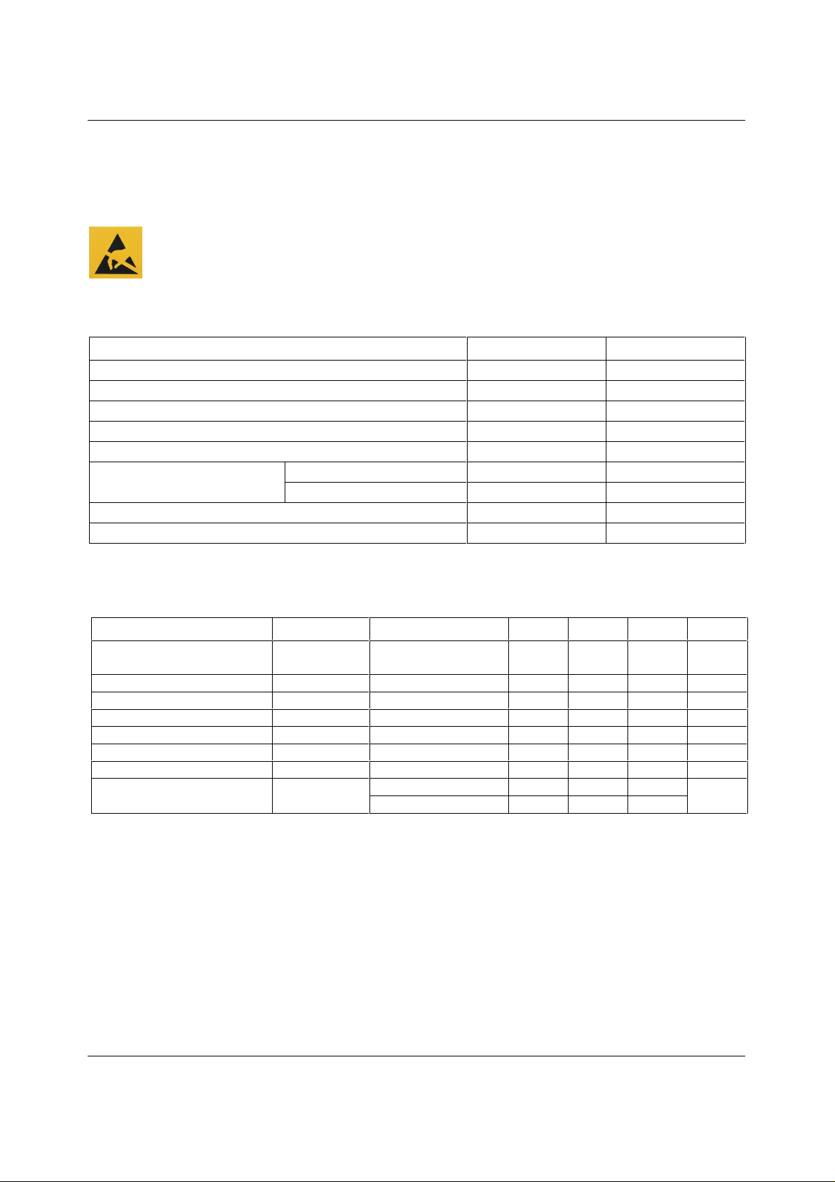
ABSOLUTE MAXIMUM RATINGS
Absolute Maximum Ratings are s tres s rat ings only. P erm anent damage to the device may be c aused by c onti nuousl y operating at
or beyond these limits. Device functional operating lim its and guaranteed performance s pecifications are gi ven under Electrical
Characteristics at the test conditions specified.
ESD Sensitive Device. Thi s device i s m anufactured on a CMOS process . It i s t herefore generi cally suscept ible
to damage from excessi ve stati c voltages . Proper ES D precautions mus t be tak en during handling and st orage
of this device.
As per JEDEC specif ic ations A112 and A 113, t his product requires s pec ifi c s torage c onditi ons pri or to s urfac e m ount ass em bly. I t
has been classified as having a Moisture Sensitivity Level of 2 and as s uch will be supplied in vacuum-sealed moisture barrier
bags.
CONDITION MIN MAX
Analogue Supply Voltage (AVDD to AGND)
Digital Supply Voltage (DVDD to DGND)
Reference Input Voltage Range (VBG )
Analogue Inputs Voltage Range
Digital Inputs Volt age Range
C suffix
Operating temperature range (TA)
I suffix
Storage temperature
Lead temperature (soldering 10 sec onds, 1.6 mm from package body)
-0.3 4 V
-0.3 4 V
AGND -0.3V AV
AGND -0.3V AV
DGND -0.3V DV
0°C+70°C
-40°C+85°C
-65°C +150°C
+0.3V
DD
+0.3V
DD
+0.3V
DD
+260°C
RECOMMENDED OPERATING CONDITIONS
PARAMETER SYMBOL TEST CONDITIONS MIN TYP MAX UNIT
Supply Voltages
(digital and analogue)
Reference Input Voltage
Digital Input HIGH Level
Digital Input LOW Level
Load Capacitance
Clock Frequency
Clock Duty Cycle
Operating Free-air Temperature
AV
, DV
DD
DD
V
f
V
V
C
CLK
BG
IH
IL
L
External reference 1.425 1.5 1.575 V
3.0 3.3 3.6 V
23.3 V
00.8V
515pF
0.1 8 8 MHz
40 50 60 %
T
A
C Suffix 0 25 70
I Suffix -40 25 85
°C
WOLFSON MICROELECTRONICS LTD PD Rev 1.1 February 2001
4
Page 5
Production Data WM2148
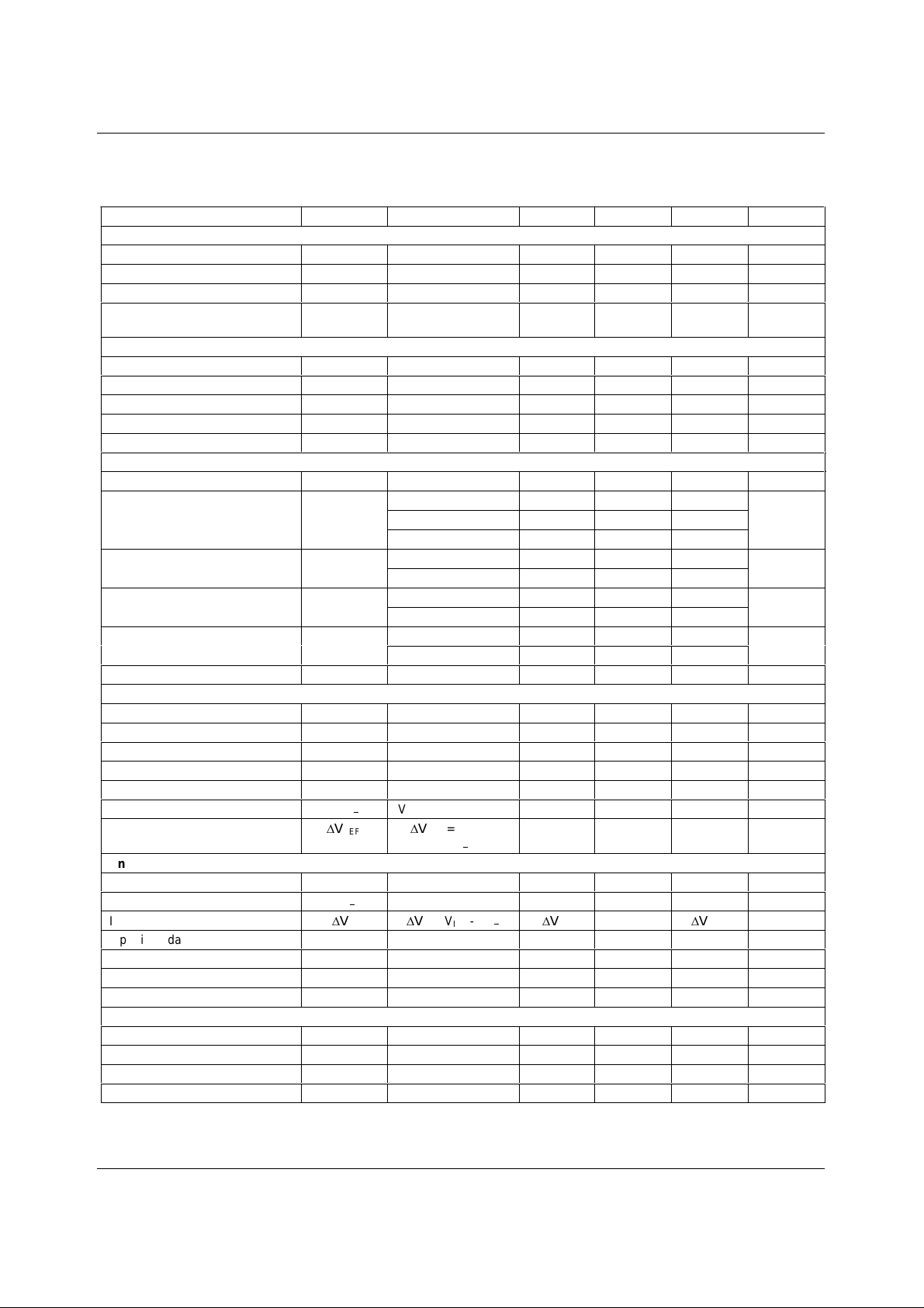
ELECTRICAL CHARACTERISTICS
Electrical characteristics over recommended temperature range, A VDD = DVDD = 3.3V (unless otherwise noted)
PARAMETER SYMBOL TEST CONDITIONS MIN TYP MAX UNIT
Power Supplies
Analogue Supply Current AI
Digital Supply Current DI
DD
DD
Power Consumption P
Power Down Supply Current
(sum of all supply c urrents)
IPD =
+DI
AI
DD
DC Characteristics
Resolution
Differential Nonlinearity DNL
Integral Nonlinearity INL
Offset Error
Gain Error
AC Characteristics
Analogue Input Bandwidth
Total Harmonic Distortion THD
Signal to Noise Ratio SNR
Signal to Noise plus Dis t ortion
SINAD
Spurious Free Dynamic Range SF DR
Effective Number of B i ts ENOB
Reference Voltage
Bandgap Voltage V
BG
Temperature Coefficient
Supply Voltage Coeffici ent
VBG Input Impedance
Positive Reference Voltage V
Negative Reference Voltage V
Reference Voltage Differenc e
¨9
REF+
REF
REF
Analog Inputs
Positive Analogue Input V ol t age V
Negative Analogue Input Voltage V
Input Voltage Difference
Input impedance Z
¨9
IN+
IN
IN
IN
PGA Range
PGA Step Size
PGA Gain Error
Digital Inputs
Input LOW level V
Input HIGH level V
Input current I
Input capacitance C
IL
IH
IN
IN
DD
í
í
AVDD = 3.6V 81 90 mA
DVDD = 3.6V 5 10 mA
AV
= DVDD = 3.6V 270 360 mW
DD
Power down mode
CLK signal stopped
20 µA
14 bits
± 0.6 ± 1 bits
Best Fit ± 3 ± 5 bits
IN+ = IN-, 0dB gain 0.3 % of FSR
0 dB gain 1 % of FSR
140 MHz
FIN = 100kHz -81
FIN = 1MHz -78
= 4MHz -77
F
IN
FIN = 1MHz 70 72
F
= 4MHz 71
IN
FIN = 1MHz 69 70
= 4MHz 70
F
IN
FIN = 1MHz 73 80
= 4MHz 80
F
IN
dB
dB
dB
dB
11.2 11.5 bits
Internal reference 1.425 1.5 1.575 V
40 ppm / °C
200 ppm / V
External reference 40 kΩ
V
= VBG (1 + 2/3)
REF+
V
= VBG (1 - 2/3)
REF+
¨9
REF
¨9
= V
IN
= V
-
REF+
V
REF
í
0AV
0AV
IN+
- V
IN
-
í
¨9
REF
2.5 V
0.5 V
2.0 V
DD
DD
¨9
REF
V
V
V
25 kΩ
07dB
1dB
± 0.25 dB
0.8 V
2V
± 1 µA
5pF
WOLFSON MICROELECTRONICS LTD PD Rev 1.1 February 2001
5
Page 6
WM2148 Production Data
Digital Outputs
Output LOW level V
Output HIGH level V
High Impedance Output Current I
OL
OH
OZ
TERMINOLOGY
1. DNL is the variation in the analogue step size associated with one digital output code across the input range,
normalised to full scale.
2. INL is the maximum deviation of the analogue input voltage associated with a digital code from its ideal value,
normalised to full s cal e. Us ing the ‘best fit’ met hod, ideal values are t aken from a strai ght line fi tted to t he ADC curve.
The INL figure thus obtained therefore characterises linearit y onl y and i s not affected by gain and offset errors.
3. SNR is the ratio in dB of signal to noise amplitude when a full -scale sine wave is applied to the input .
4. THD is the ratio in dB of the s um of all harmonics to signal amplitude when a full sc ale sine wave is applied to the
input.
5. SFDR is the amplitude ratio the output signal to the largest spur (artifact ) produced by the device.
I
= -50µA0.4V
OUT
I
= +50µA2.6 V
OUT
±10 µA
ANALOGUE
INPUT
S1
S0
S2
S3
S5
S4
S6
S7
S9
S10
S8
S11
S12
S13
S14
S15
S16
CLK
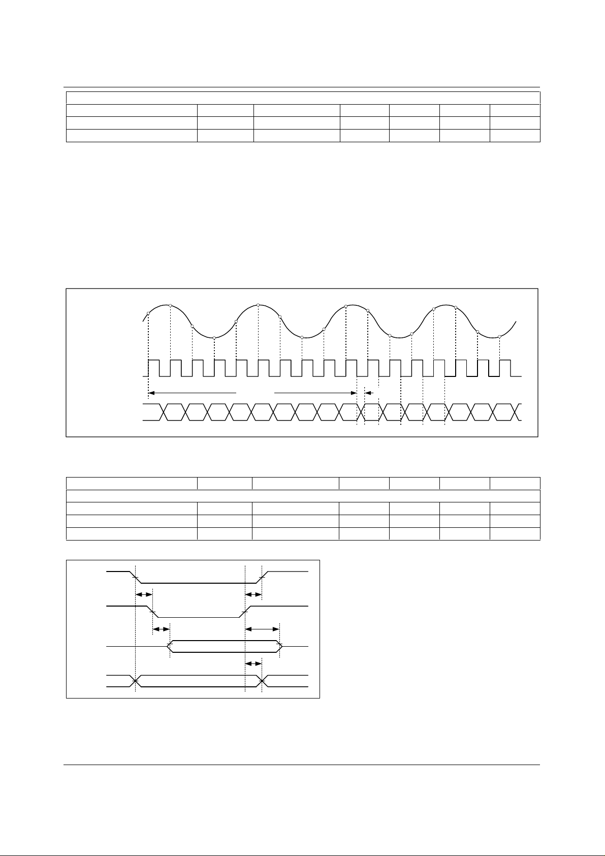
OUTPUT DATA
012345678910111213
Latency
t
d
S0 S1 S2 S3 S4 S5 S6
14 15
16
Figure 1 Latency
PARAMETER SYMBOL TEST CONDITIONS MIN TYP MAX UNIT
Clock Timing
Clock Frequency f
Output Delay Time t
Latency
CLK
d
CS = Low 0. 1 8 8 MHz
CS = Low 25 ns
CS = Low 9.5 cycles
CSB
t
su(OE-ACS)
t
h(CS)
OEB
t
h(A)
t
dis
D[0:13]
A[0:1]
t
en
DATA
XX
ADDRESS
Figure 2 Read Timing
WOLFSON MICROELECTRONICS LTD PD Rev 1.1 February 2001
6
Page 7
Production Data WM2148
PARAMETER SYMBOL TEST CONDITIONS MIN TYP MAX UNIT
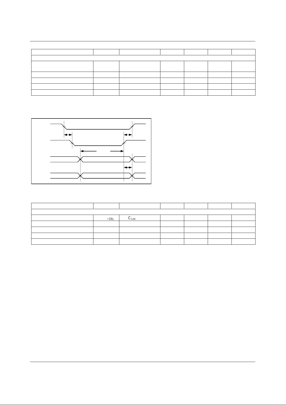
Read Timing
Address and Chip select S etup
t
su(OE-ACS)
C
= 15pF 4 ns
Load
Time
Output Enable
Output Disable
Address Hold Time
Chip select Hold Time
t
t
t
h(A)
t
h(CS)
C
en
dis
= 15pF 15 ns
Load
C
= 15pF 10 ns
Load
C
= 15pF 1 ns
Load
C
= 15pF 0 ns
Load
Note:
1. All timing parameters refer to a 50% level.
CSB
t
su(WE-CS)
t
h(CS)
WEB
t
su(DA)
A[0:1]
XD[0:13]
XX
DATA
ADDRESS
t
h(CS)
X
Figure 3 Write Timing
PARAMETER SYMBOL TEST CONDITIONS MIN TYP MAX UNIT
Write Timing
Chip Select Setup Time
Data and Address Setup Time
Data and Address Hold Time
Chip Select Hold Time
Write Puls e Duration HIGH
t
su(WE
t
í&6
t
su(DA)
t
h(DA)
t
h(CS)
wH(WE)
C
= 15pF 4 ns
Load
C
= 15pF 29 ns
Load
C
= 15pF 0 ns
Load
C
= 15pF 0 ns
Load
C
= 15pF 15 ns
Load
Note
1. Data is written to the addressed register at the rising edge of WEB. All t i ming parameters refer to a 50% level.
WOLFSON MICROELECTRONICS LTD PD Rev 1.1 February 2001
7
Page 8
WM2148 Production Data DEVICE DESCRIPTION
INTRODUCTION
The WM2184 is a fast, low-power 14-bit ADC designed for leading edge telecommunications
applications such as xDSL front-ends. It consists of a high bandwidth programmable gain input
stage, a high resolution ADC, a parallel control int erface, and int ernal voltage referenc e circuit ry. Its
fully differential design gi ves it excellent noise im munity.
The analogue signal first enters the programmable gain amplifier (PGA), whose gain can be
controlled in 1dB steps between 0dB and 7dB, using the PGA gain register. The signal is then
digitised with respect to the two reference voltages, V
compensate for DC off sets in the system, a program mable value of between -128 and +127 LSBs
can be added to the digitised data. This is achieved by writing the offs et value to the offset regi ster
and setting the DCO bit (bit 7) i n t he control register.
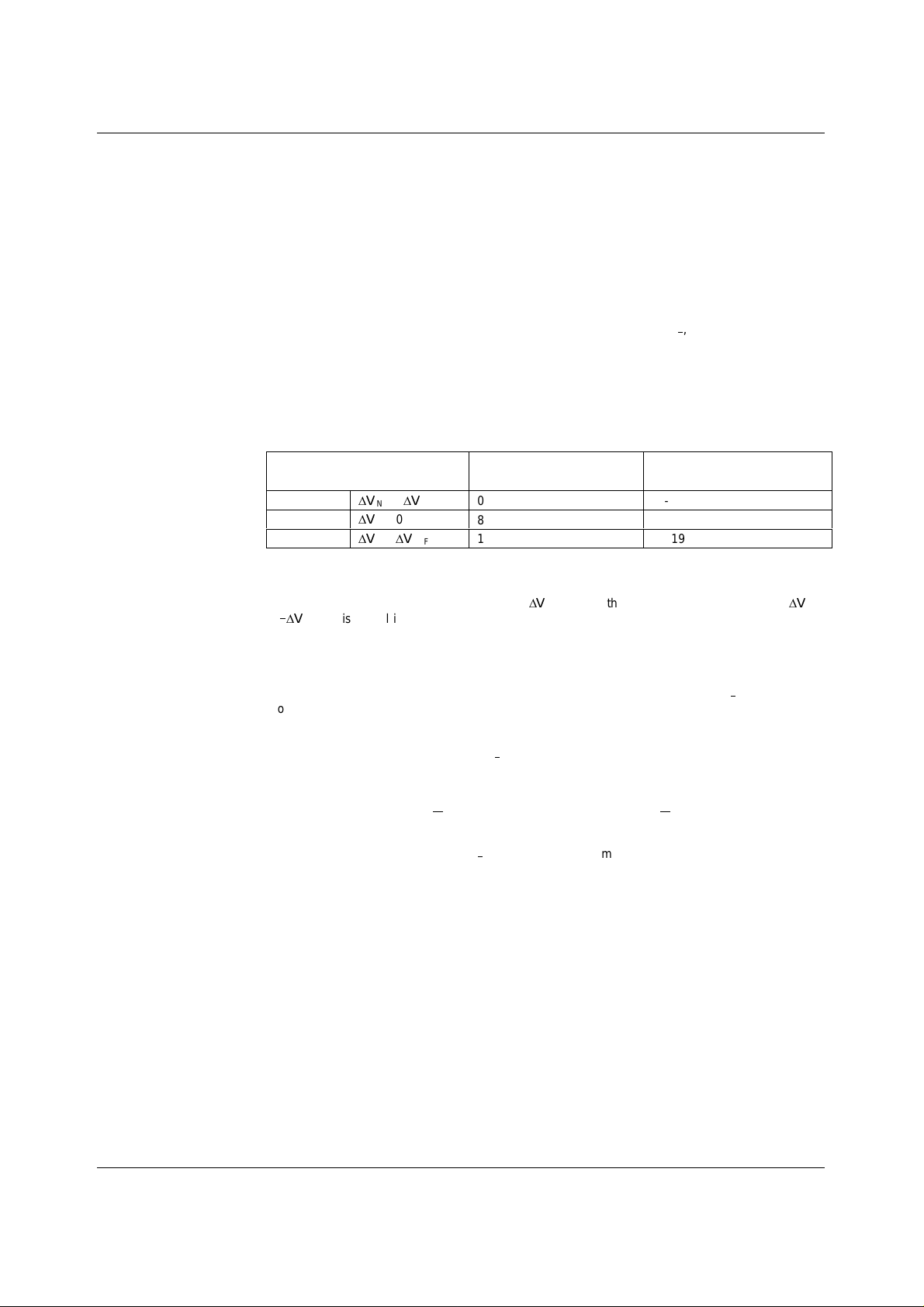
Two different output formats are supported to suit the user’s needs. I n unsi gned binary format, an allzero output represents the m inimum analogue input level, while i n two’s comp lement form at it refers
to the middle level between mi ni mum and maximum (see Table 1, below).
REF+
and V
, in the ADC core. To
REF
í
ANALOGUE INPUT DIGITAL OUTPUT
(Unsigned Binary)
Minimum
Midrange
Maximum
¨9
¨9
¨9
= -
¨9
IN
REF
= 0
IN
=
¨9
IN
REF
0 -8192
8192 0
16383 8191
DIGITAL OUTPUT
(Two’s Complement)
Table 1 Unsigned Binary vs Two’s Complement Output Format
The out-of-range indicator (OVI) output indicates that the anal ogue input signal is out of range. It is
asserted whenever the differential input volt age
or
í¨9
. This signal is updated simultaneous ly with the digital data outputs and is s ubject to the
REF
exceeds the differential reference vol tage
IN
¨9
REF
¨9
same pipeline delay. It can be used to adjust the gain of the internal PGA t o prevent the ADC from
clipping.
The WM2148 incorporates a differential voltage reference circuit based on a 1.5V bandgap
reference. The two reference voltages derived from the bandgap, V
above and below the bandgap voltage V
, at 2.5V and 0.5V respect ively. The analogue input range
BG
REF+
and V
, are two-thirds
REF
í
is between the two references. To use an external reference, the on-chi p bandgap circuit i s disabled
by setting the REF bit (bit 12) in the control register. The external reference voltage can then be
applied at the VBG pin. V
REF+
and V
are still buffered in the same by the internal reference
REF
í
amplifiers, such that:
VV
1
+
BGREF
For best performance, VBG, V
2
+×=
3
REF+,VREF
and
and CML (reference midpoint, pin 4) s hould all be s eparatel y
í
VV
−
BGREF
2
−×=
1
3
decoupled (see Recomm ended E xternal Components).
The WM2184 requires a single 3.3V supply voltage. I n Power Down mode, t he suppl y to all analogue
circuitry in the device is switched off, reducing standby current to 20µA provided that t he clock is
stopped (a running clock will increase the power consum ption of the digital sections).
CONTROL INTERFACE
All functions of the WM2184 are accessed through its parallel interface. There are four internal
registers to retrieve the A DC conversion data, set the devic e gain and DC offset, and c ontrol other
features such as Power Down, reference voltage and output format.
The parallel interface of the W M2148 features three-state buff ers for direct connection to a shared
data bus. Driving the OEB pin low enables t he output buffers.
WOLFSON MICROELECTRONICS LTD PD Rev 1.1 February 2001
8
Page 9
Production Data WM2148
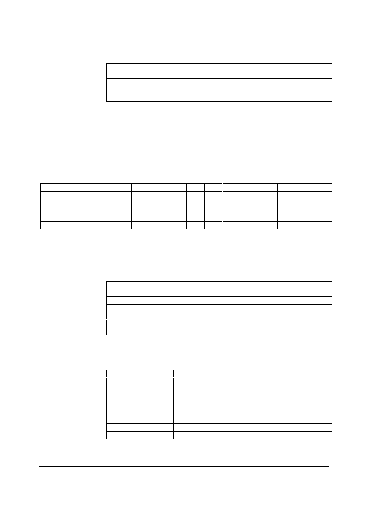
ADDRESS A1 A0 REGISTER
0 0 0 ADC Conversion Result
1 0 1 PGA gain
2 1 0 DC Offset
3 1 1 Control
Table 2 WM2148 Internal Registers
The ADC data register contains the res ult of the last analogue to digital c onversion. It can also be
used to reset the device to its default stat e by writing a ‘1’ to the LSB (D0). This will set all the bits in
the gain, offset and cont rol registers to ‘0’. A ll other bit s shoul d always be set to zero when writing to
the ADC data register.
The PGA gain is controlled using the last three bits of Address 1. The eight pos sible binary val ues of
000 to 111 (decimal 7) correspond t o a gai n of 0 to 7dB, respectively.
The lower byte of Address 2 holds the offset value (in LSBs ). This value is added to the ADC data if
the DCO bit in the Control register is s et. The offset is in Two’s complement form at, providing a
range of -128 to +127 LSB.
REG. / BITD13D12D11D10D9D8D7D6D5D4D3D2D1D0
ADC Data MSB ………………………………LSB/
SR
PGA GainXXXXXXXXXXXG2G1G0
DC Offset X X X X X X MSB ………………LSB
ControlPWDREFFORTM2TM1TM0DCOXXXXXXX
Table 3 WM2148 Register Map
The Control register (address 3) has f our bits t o program the devi ce’s operat ion and three test m ode
bits. Setting the P ower Down bit (PWD) tak es the device into P ower Down mode. DCO enables the
addition of the offset value held at Address 2 to the ADC out put data. REF selec ts between internal
and external reference voltages, and FOR between unsigned binary and Two’s com plement output
format.
BIT DESCRIPTION 0 1
PWD Power Down Normal Operati on Power Down
REF Reference Select Internal Reference External Reference
FOR Output Format Unsigned B i nary Two’s Complement
DCO DC Offset Enable Disable
SR Software Reset Normal Operat i on Reset
X Reserved A l ways s et to 0 when writing to any register.
Table 4 Control Bits and Software Reset
The ADC core can be tested by selecting one of six different test modes, which apply various
voltages to the analogue inputs. This may be useful for calibration purpos es. The test modes are
controlled by the three test mode bits in the control regi ster, TM0 to TM2 (see Table 5 below).
TM2 TM1 TM0 FUNCTION
0 0 0 Normal Operation
0 0 1 Both inputs = REF010IN+ at V
/2, IN- at REF-
ref
0 1 1 IN+ at REF+, IN- at REF1 0 0 Normal Operation
1 0 1 Both inputs = REF+
1 1 0 IN+ at REF-, IN- at V
/2
ref
1 1 1 IN+ at REF-, IN- at REF+
Table 5 Test Modes
WOLFSON MICROELECTRONICS LTD PD Rev 1.1 February 2001
9
Page 10
WM2148 Production Data
PERFORMANCE DATA (TYPICAL)
284
282
280
278
276
274
Power [mW]
272
270
268
0.1 1 10
Frequency [MHz]
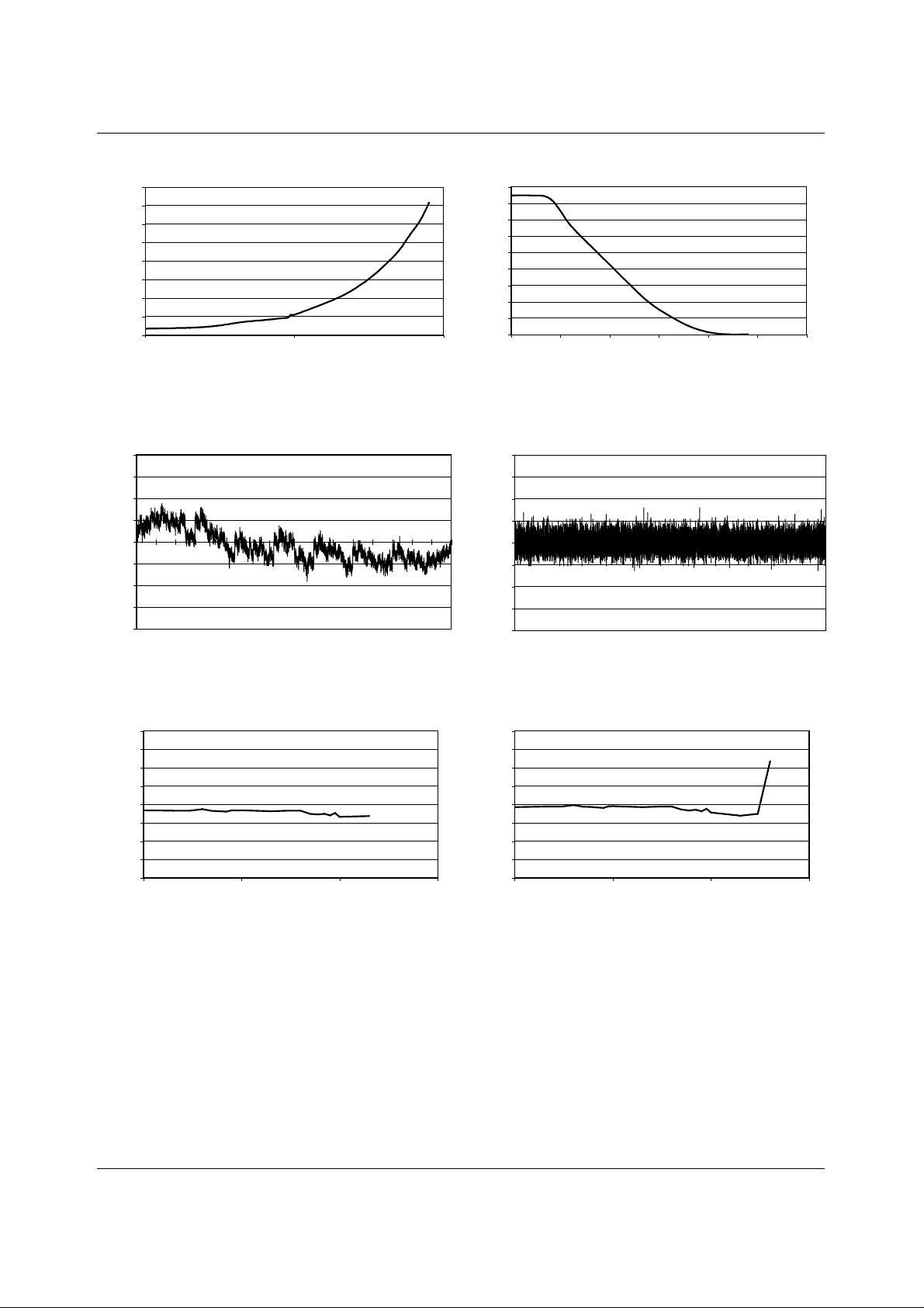
Figure 4 Power Consumption vs Sample Clock
8
6
4
2
0
INL (LSBs)
-2
-4
-6
-8
-8192 -6144 -4096 -2048 0 2048 4096 6144
Code
90
80
70
60
50
40
30
DIDD+AIDD [mA]
20
10
0
0 50 100 150 200 250 300
time [ns]
Figure 5 Supply Current vs Time (Power Down)
2
1.5
1
0.5
0
DNL (LSBs)
-0.5
-1
-1.5
-2
-8192 -6144 -4096 -2048 0 2048 4096 6144
Code
Figure 6 Integral Nonlinearity at 8MSPS
-74
-76
-78
-80
-82
THD [dB]
-84
-86
-88
-90
10 100 1000 10000
Signal Frequency [kHz] at -1dB
Figure 8 Total Harmonic Distortion at 3MSPS
Figure 7 Differential Nonlinearity at 8MSPS
-74
-76
-78
-80
-82
THD [dB]
-84
-86
-88
-90
10 100 1000 10000
Signal Frequency [kHz] at -1dB
Figure 9 Total Harmonic Distortion at 8MSPS
WOLFSON MICROELECTRONICS LTD PD Rev 1.1 February 2001
10
Page 11
Production Data WM2148
75
74
73
72
71
SNR [dB]
70
69
68
67
10 100 1000 10000
Signal Frequency [kHz] at -1dB
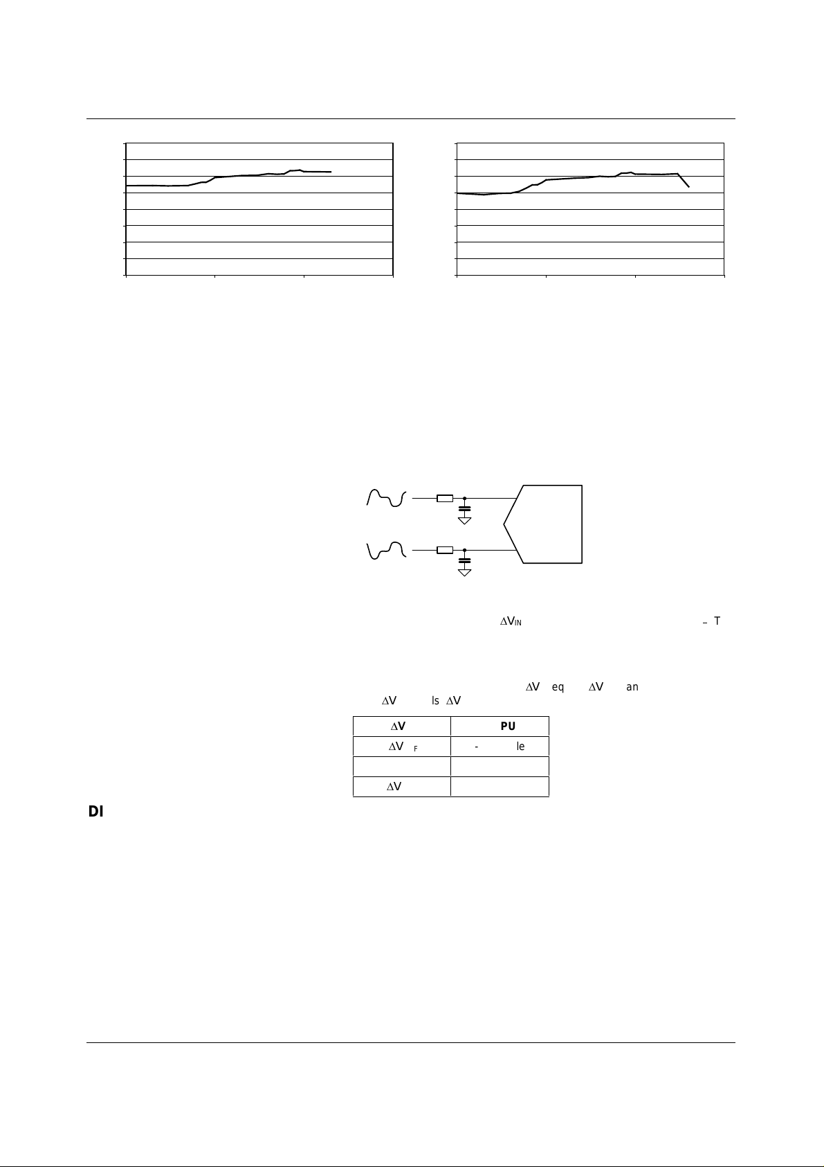
Figure 10 Signal to Noise Ratio at 3MSPS
APPLICATION INFORMATION
DRIVING THE ANALOGUE INPUT
The WM2148 has a fully differential input. This is advant ageous for signal to noise ratio, spurious
free dynamic range, and harmoni c distortion. It is recommended that t he anal ogue input pins IN+ and
IN- are connected as shown in Figure 12 below.
DIFFERENTIAL
ANALOGUE
INPUT
75
74
73
72
71
SNR [dB]
70
69
68
67
10 100 1000 10000
Signal Frequency [kHz] at -1dB
Figure 11 Signal to Noise Ratio at 8MSPS
22 Ohms
100pF
22 Ohms
100pF
IN+
WM2148
IN-
DIGITAL I/O
Figure 12 Recommended Input Configuration
In this configuration, the A DC convert s t he dif ferenc e
¨9
of the two input signals V
IN
IN+
and V
IN
. The
í
resistors and capacitors on the inputs decouple the driving source output from the A DC and also
serve as first order low pass f i l t ers to reduce out of band noise.
The input range on both inputs is 0V to AV
reference. The positive full-s cale output is reached when
¨9
scale output is reached when
IN
¨9
-
¨9
equals -
IN
REF
. The full-scale value is determined by the voltage
¨9
DD
REF
.
¨9
equals
IN
¨9
, and the negative full-
REF
OUTPUT
- full scale
00
¨9
REF
+ full scale
The digital outputs of the WM2148 are 3V CMOS compat ible. In order to avoid current feedback
errors, the capacitive load on t hese outputs should be as low as pos sible (maximum 15pF). Adding
100Ω series resistors on the digit al outputs c am im prove system performance by l imiti ng the current
during output transitions (t hi s reduces noise on the power supplies).
WOLFSON MICROELECTRONICS LTD PD Rev 1.1 February 2001
11
Page 12
WM2148 Production Data
RECOMMENDED EXTERNAL COMPONENTS
AVDD DVDD
+
C1
AGND
AGND
AGND
AGND
DIFFERENTIAL
ANALOGUE
INPUT
C2
C4 C5
C6
C7
AGND
43
44
47
46
45
48
2
7
1
AVDD
AGND
AVDD
AGND
AVDD
AGND
AGND
WM2148
IN+
IN-
DVDD
DGND
DVDD
DGND
DVDD
DGND
DVDD
DGND
DVDD
DGND
DVDD
31
33
30
9
42
34
14
15
25
26
20
C9C3
C10
C11
C12
C13
DGND
DGND
DGND
DGND
DGND
C8
DGND
+
+
C14 C15
AGND
AGND
AGND
AGND
C17 C18
C19 C20
C16
+
+
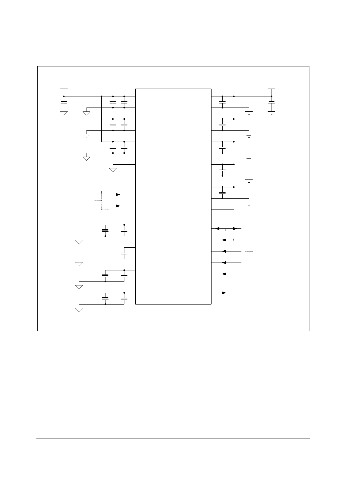
Figure 13 External Components Diagram
3
VBG
4
CML
5
REF+
6
REF-
D[0:13]
A[0:1]
OEB
WRB
CSB
OVI
35
36
37
10
14
2
CONTROL BUS
OUT OF RANGE
INDICATOR
WOLFSON MICROELECTRONICS LTD PD Rev 1.1 February 2001
12
Page 13

Production Data WM2148
COMPONENT
REFERENCE
C1 10µF Analogue Supply Decoupling
C2 0.1µF Supply Decoupling for Ref erence Block
C3 470pF Supply Decoupling for Reference B l ock - place as close t o the IC as possible
C4 0.1µF Supply Decoupling for A DC
C5 470pF Supply Decoupling for ADC - plac e as close to the IC as pos sible
C6 0.1µF Supply Decoupling for A DC Op-amps
C7 470pF Supply Decoupling for ADC Op-amps - place as close t o the IC as possible
C8 10µF Digital Supply Decoupling
C9 0.1µF Supply Decoupling Cloc k Buffers - place as c l ose to the IC as possibl e
C10 0.1µF Supply Decoupling for Core Logic
C11 0.1µF Supply Decoupling for Control Block
C12, C13 0.1µF Supply Decoupling f or Output Drivers
C14, C17, C19 10µF Reference Decoupling
C15, C16, C18, C20 0.1µf Ref erence Decoupling - place as clos e t o t he IC as possible
Table 6 External Components Values and Description
SUGGESTED
VALUE
DESCRIPTION
(most critical for ADC performance)
to eliminate cloc k jitter
WOLFSON MICROELECTRONICS LTD PD Rev 1.1 February 2001
13
Page 14
WM2148 Production Data PACKAGE DIMENSIONS
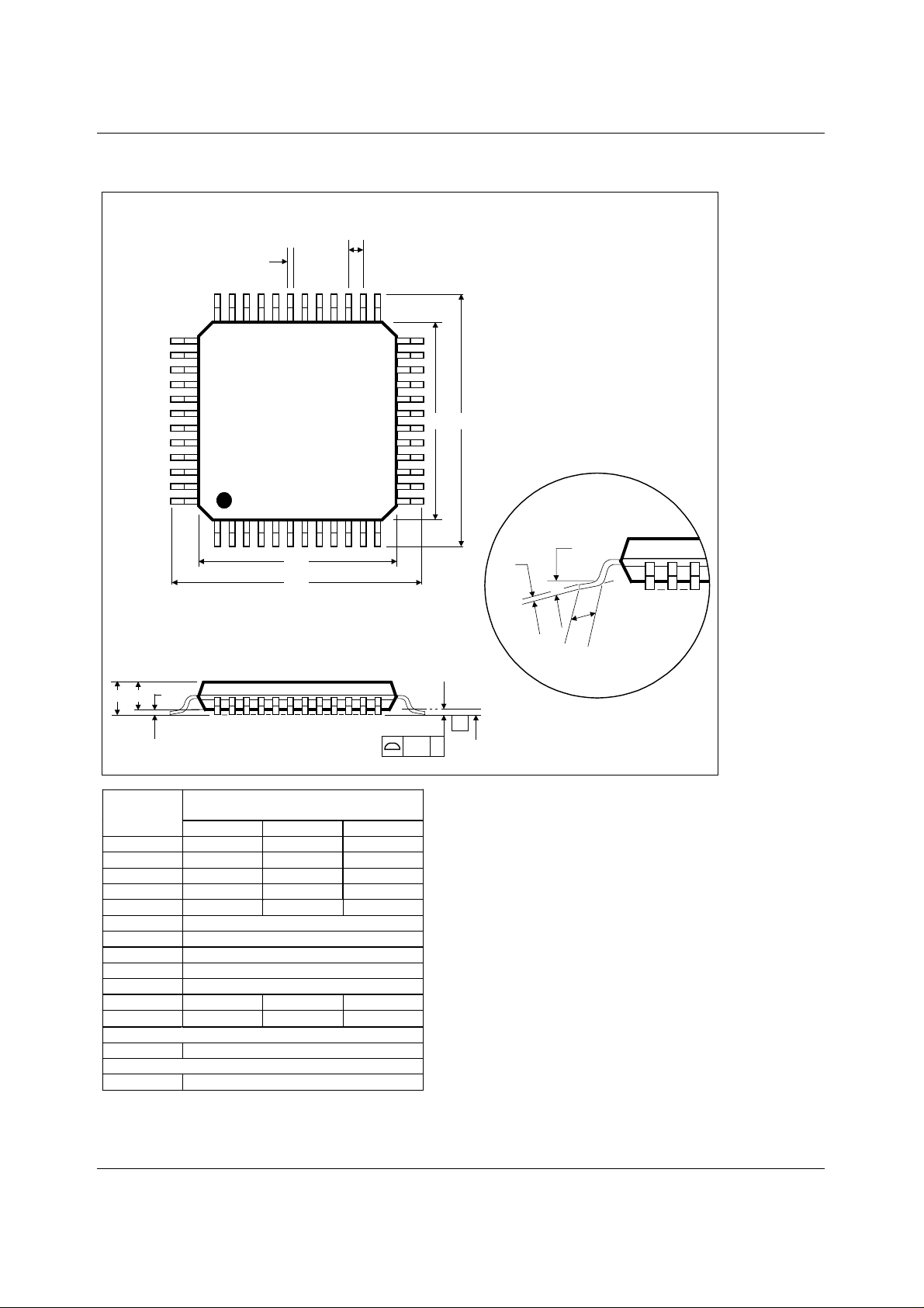
FT: 48 PIN TQFP (7 x 7 x 1.0 mm)
b
48
D1
D
DM004.C
e
2536
2437
E1 E
13
121
c
Θ
L
A1
A2
A
-C-
SEATING PLANE
C
ccc
Dimensions
Symbols
(mm)
MIN NOM MAX
A
A
1
A
2
b
c
D
D
1
E
E
1
e
L
Θ
----- ----- 1.20
0.05 ----- 0.15
0.95 1.00 1.05
0.17 0.22 0.27
0.09 ----- 0.20
9.00 BSC
7.00 BSC
9.00 BSC
7.00 BSC
0.50 BSC
0.45 0.60 0.75
o
0
3.5
o
7
o
Tolerances of Form and Position
ccc
REF:
NOTES:
A. ALL LINEAR DIMENSIONS ARE IN MILLIMETERS.
B. THIS DRAWING IS SUBJECT TO CHANGE WITHOUT NOTICE.
C. BODY DIMENSIONS DO NOT INCLUDE MOLD FLASH OR PROTRUSION, NOT TO EXCEED 0.25MM.
D. MEETS JEDEC.95 MS-026, VARIATION = ABC. REFER TO THIS SPECIFICATION FOR FURTHER DETAILS.
0.08
JEDEC.95, MS-026
WOLFSON MICROELECTRONICS LTD PD Rev 1.1 February 2001
14
 Loading...