

Page 1

W83320S/W83320G
Winbond
N-Channel FET Synchronous Buck
Regulator Controller
W83320S
W83320G
Publication Release Date: January 10, 2006
- 1 - Revision 0.51
Page 2
W83320S/W83320G
W83320S
Data Sheet Revision History
PAGES DATES VERSION
1 N.A. N.A. 0.50 N.A.
2 N.A. N.A. 0.51 N.A. Add Pb-free part no :W83320G
VERSION
ON WEB
MAIN CONTENTS
All version before 0.5 are for internal use
only.
Please note that all data and specifications are subject to change without notice. All the trademarks of
products and companies mentioned in this datasheet belong to their respective owners.
LIFE SUPPORT APPLICATIONS
These products are not designed for use in life support appliances, devices, or systems where
malfunction of these products can reasonably be expected to result in personal injury. Winbond
customers using or selling these products for use in such applications do so at their own risk and
agree to fully indemnify Winbond for any damages resulting from such improper use or sales.
- 2 -
Page 3

W83320S/W83320G
Table of Content-
1. GENERAL DESCRIPTION ......................................................................................................... 4
2. FEATURES ................................................................................................................................. 4
3. APPLICATIONS .......................................................................................................................... 4
4. PIN-OUT ..................................................................................................................................... 5
5. PIN DESCRIPTION..................................................................................................................... 6
6. INTERNAL BLOCK DIAGRAM ................................................................................................... 7
7. APPLICATION CIRCUIT............................................................................................................. 9
8. ELECTRICAL CHARACTERISTICS......................................................................................... 10
9. TYPICAL PERFORMANCE CHARACTERISTICS................................................................... 11
10. PACKAGE DIMENSION OUTLINE........................................................................................... 16
11. ORDERING INSTRUCTION ..................................................................................................... 17
12. HOW TO READ THE TOP MARKING...................................................................................... 17
Publication Release Date: January 10, 2006
- 3 - Revision 0.51
Page 4

W83320S/W83320G
1. GENERAL DESCRIPTION
The W83320S is a high-speed, N-Channel synchronous buck regulator controller optimized for wide
reference input range. The W83320S employs adjustable frequency ranging from 100 KHz to 400 KHz
voltage-mode PWM control architecture. The regulator is biased from a 5V rail and the power for the
high-side MOSFET can be supplied by a separate 12V rail or supplied from the internal charge pump.
A Current limit protection is implemented by monitoring the voltage drop across the switch ON
resistance of the low-side MOSFET. This method can eliminate the requirement of extra current
sensing resistor and avoids false trigger of OC protection when V
non-overlapping MOSFET gate drivers help avoid potential shoot-through problems while maintaining
high efficiency. All these together with Power-good flag, enable and soft start features make power
sequencing easy.
2. FEATURES
y 1.8V to 5V power stage input voltage
y Providing +/-1.5% reference voltage
y Power Good flag
y Current limit without sense resistor
y Soft start
y Switching frequency from 100 kHz to 400 kHz
y Tiny plastic SOP-14 package
varies efficiently. The adaptive
IN
3. APPLICATIONS
y DDR SDRAM and AGP core power for Desktop PC
y Set-Top Boxes/ Home Gateways
y Core Logic Regulators
y High-Efficiency Buck Regulation
- 4 -
Page 5
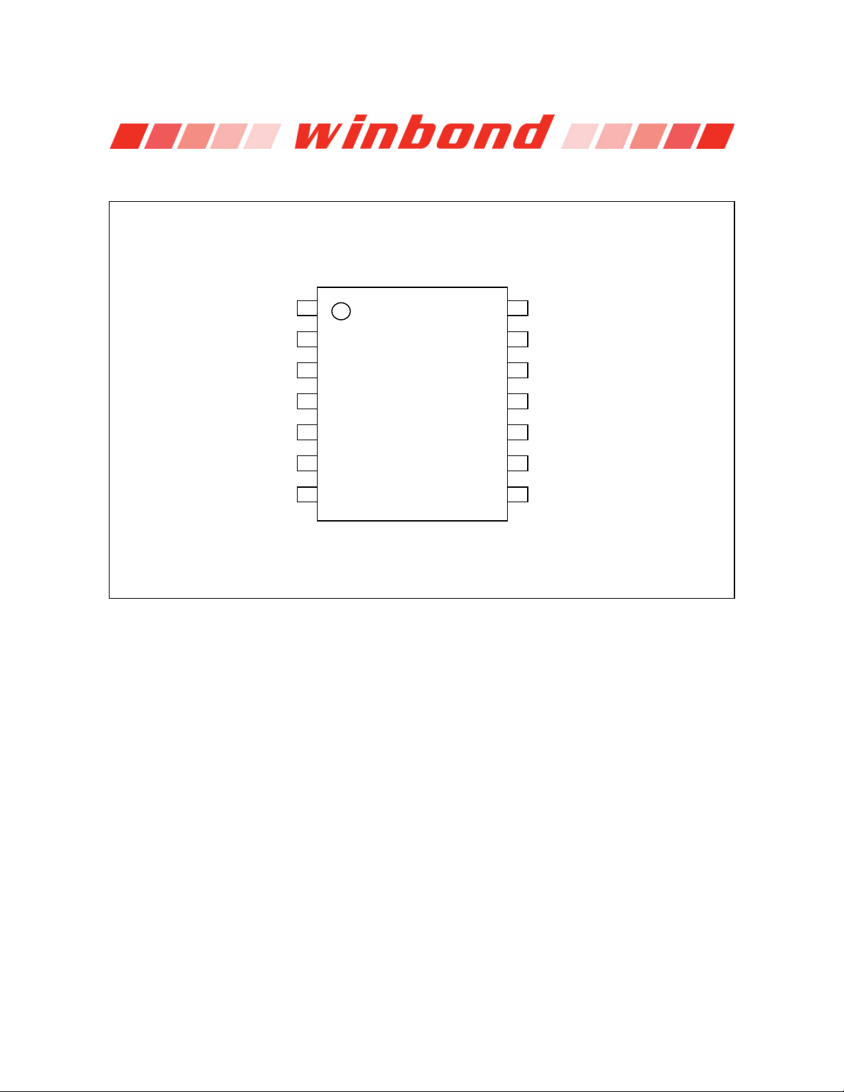
4. PIN-OUT
3
5
6
3
0
9
W83320S/W83320G
LGATE
VDD
VDDA
PWOK
GNDA
1
14
I
SEN
1
12
11
1
GND
UGATE
BOOT
BG_REF
2
4
W83320S
SS
COMP
7
V
REF
8
FB
Publication Release Date: January 10, 2006
- 5 - Revision 0.51
Page 6
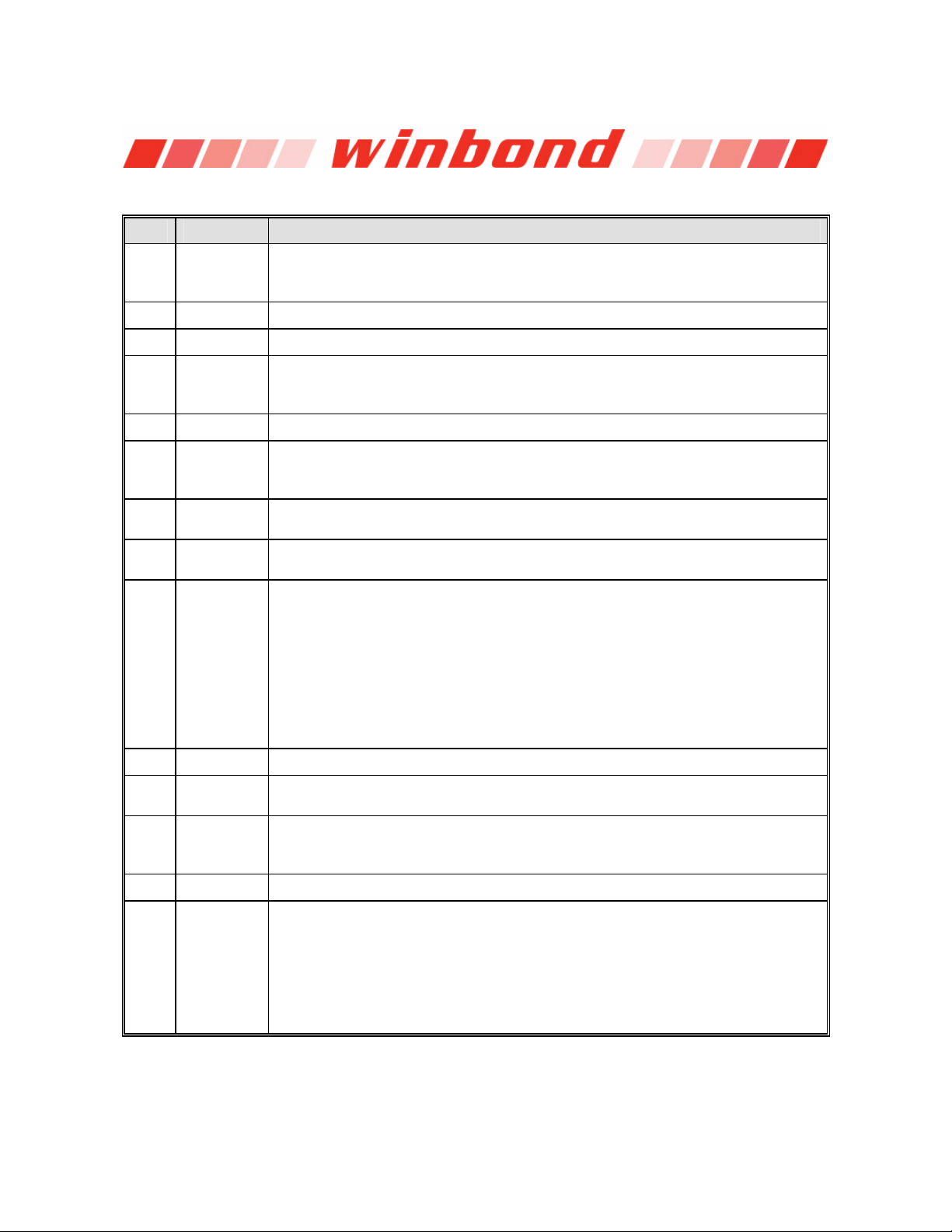
5. PIN DESCRIPTION
PIN NAME FUNCTION
Low-Side N-Channel MOSFET Gate Drive Pin. This pin is monitored by the
1
2
LGATE
VDD
adaptive shoot-through protection circuitry to determine when the low-side
MOSFET turned off.
+5V supply rail for the lower gate driver and control logic circuit.
W83320S/W83320G
3
VDDA
VDDA: +5V supply rail for the chip.
Power OK. Open drain output. This pin will be opened in following conditions:
4
PWROK
1. No over-current detected; 2. V
_IN >0.6V; 3. FB > 75% of V
REF
_IN; 4. SS
REF
>3V.
5
GNDA
Ground for analog circuit. Connect it to system ground.
Soft Start Pin. A capacitor should be attached in this pin to ground for soft start
6
SS
output clamping. This capacitor, along with an internal 12uA current source,
set the output clamp ramp up speed.
7
8
COMP
FB
Internal Error Amplifier Output Pin. This pin is available for compensation of
the control loop.
Inverting Input of the Error Amplifier. This pin is available for compensation of
the control loop.
Non-inverting Input of the Error Amplifier. Voltage on this pin provides
reference input to the PWM control loop.
When the V
_IN voltage is less than 0.27V, the PWM is shut-down and the
REF
H_DRV and L_DRV are driven low. Due to its wide input range (0 ~ 3.6V), the
9
V
REF
_IN voltage can be raised slowly to perform the input clamp function.
V
REF
Besides, a special function is implemented in this IC to inform the reference
provider of over current alarm. Each time as the OC occurs, V
_IN will be
REF
short to GND (through 170 ohms) for about 5~10uS. The reference provider
can be aware of the OC condition by detecting this pulse.
10
11
BG_REF
BOOT
Internal Bandgap Reference Voltage Output.
Supply rail for the high-side MOSFET driver. A bootstrap circuit may be used
to create a BOOT voltage or a separate 12V supply can be used.
High-Side N-Channel MOSFET Gate Drive Pin. This pin is also monitored by
12
UDRV
the adaptive shoot through protection circuitry to determine when the high-side
MOSFET has turned off.
13
GND
Ground for signal level circuit. Connect it to system ground.
Current limit threshold setting. Connect a resistor (R
OCSET
) between this pin
and the drain of the low-side MOSFET. An internal 72uA current source will
and cause a fixed voltage drop on it while the low-side
ISEN
14
I
SEN
flow through R
MOSFET is turned on. In the mean while, the W83320S compares the voltage
drop with the voltage across the low-side MOSFET and determines whether
the current limit has been reached. The equation for over-current limit is:
I
= (72uA * R
LIM
ISEN
)/R
DSON
- 6 -
Page 7
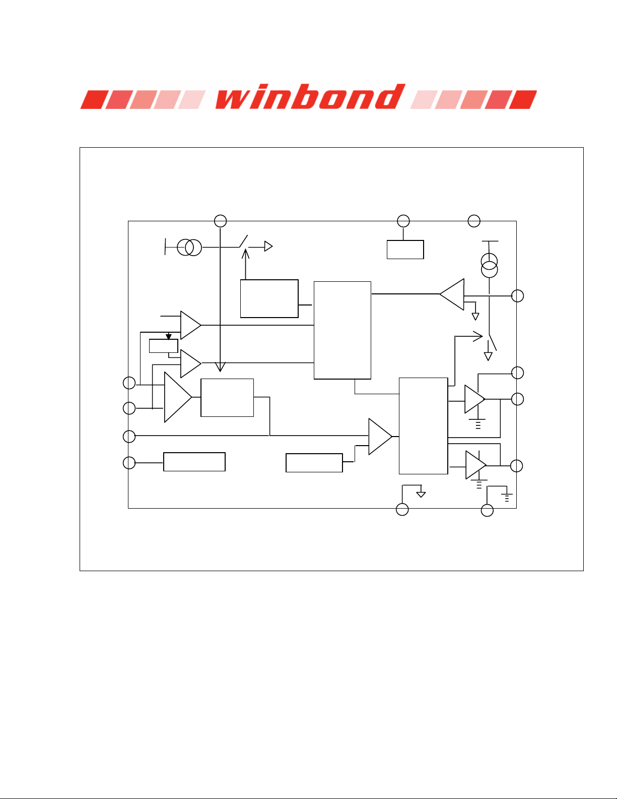
6. INTERNAL BLOCK DIAGRAM
SS
S
W83320S/W83320G
V
REF
FB
COMP
BG_REF
0.6V
X0.7
.
.
12µA
+
EA
-
I
REF
& V
.
Output
Clamp
REF
Soft Start
Logic
.
Control
Oscillator
Logic
VDDA VDD
POR
Gate
+
-
Control
Logic
72µA
VDD
.
.
.
I
EN
BOOT
UGATE
LGATE
GND GNDA
Publication Release Date: January 10, 2006
- 7 - Revision 0.51
Page 8

W83320S/W83320G
Soft-Start
When V
capacitor begins to charge through an internal 12uA (I
the PWM duty) is both output clamped by the voltage on soft-start pin V
voltage on V
between V
is triggered to work. 0.4V to 1.9V of V
0.27V on V
MOSFET Gate Drivers
The power for the high-side driver is flowing through the BOOT pin. This voltage can be supplied by a
separate, higher voltage source, or supplied from a local charge pump structure or combination of the
two.
Since the voltage of the low-side MOSFET gate and the high-side MOSFET gate are being monitored
to determine the state of the MOSFET, it should be taken carefully to add external components
between the gate drivers and their respective MOSFET gates. Doing so may interfere with the shootthrough protection.
Current Limit
Current limit is implemented by sensing the voltage across the low-side MOSFET while it is ON. This
method enhances the converter's efficiency and reduces total cost by eliminating a current sensing
resistor.
While low-side MOSFET is turned on, a constant current of 72uA (IREF X 3) is forced through
ROCSET which is an external resistor connected between phase and ISEN, causing a fixed voltage
drop. This fixed voltage is compared against VDS and if the latter is higher, the chip enters current
limit mode. In the current limit mode both the high-side and low-side MOSFETS are turned off and the
soft start capacitor CSS will be discharged immediately. The VREF is shorted to GND for 5~10uS to
indicate the over current condition. After a 5mS delay, a soft-start cycle is initiated. If the cause of the
over-current is still present after the delay interval, the current limit would be triggered again. The shut
down - delay - soft start cycle will be repeated indefinitely until the over-current event been removed.
and VDD ramp over 4.3V and the voltage at pin V
DDA
REF
. There are two ways to soft start the power that’s following the rising of the slower one
REF
SS
REF
or V
; during soft-start, PWOK is forced to low and the internal Over-Current Protection
REF
is roughly mapping to 0 to 100% pulse-width. Smaller than
SS
will disable the PWM controller and discharge CSS.
ramps over 0.27V; the soft start
REF
/2) current source. The error amplifier (and
and input clamped by the
SS
Input Tracking
When the VREF voltage is less than 0.3V, the PWM is shut-down and the UGATE and LGATE are
driven low. Due to its wide input range (0 ~ 3.6V), this chip is suitable for reference input tracking
application. But note that the chip will be shut-down when VREF <0.27V, a proper setting of CSS is
needed to clamp the output at initiation of start up and avoid output voltage step-up ( and so a large
inrush current).
I
and PWM Clock
REF
The Internal reference current (IREF) is determined by the resistor between pin BG_REF pin and
GND (RSET) according to the following equation:
I
= 1.19V/Rset
REF
The nominal 200 kHz PWM clock can be adjusted ranging form 100 kHz to 400 kHz by changing IREF
according to the following equation:
Freq = 200 KHz * I
/ 24uA;
REF
- 8 -
Page 9
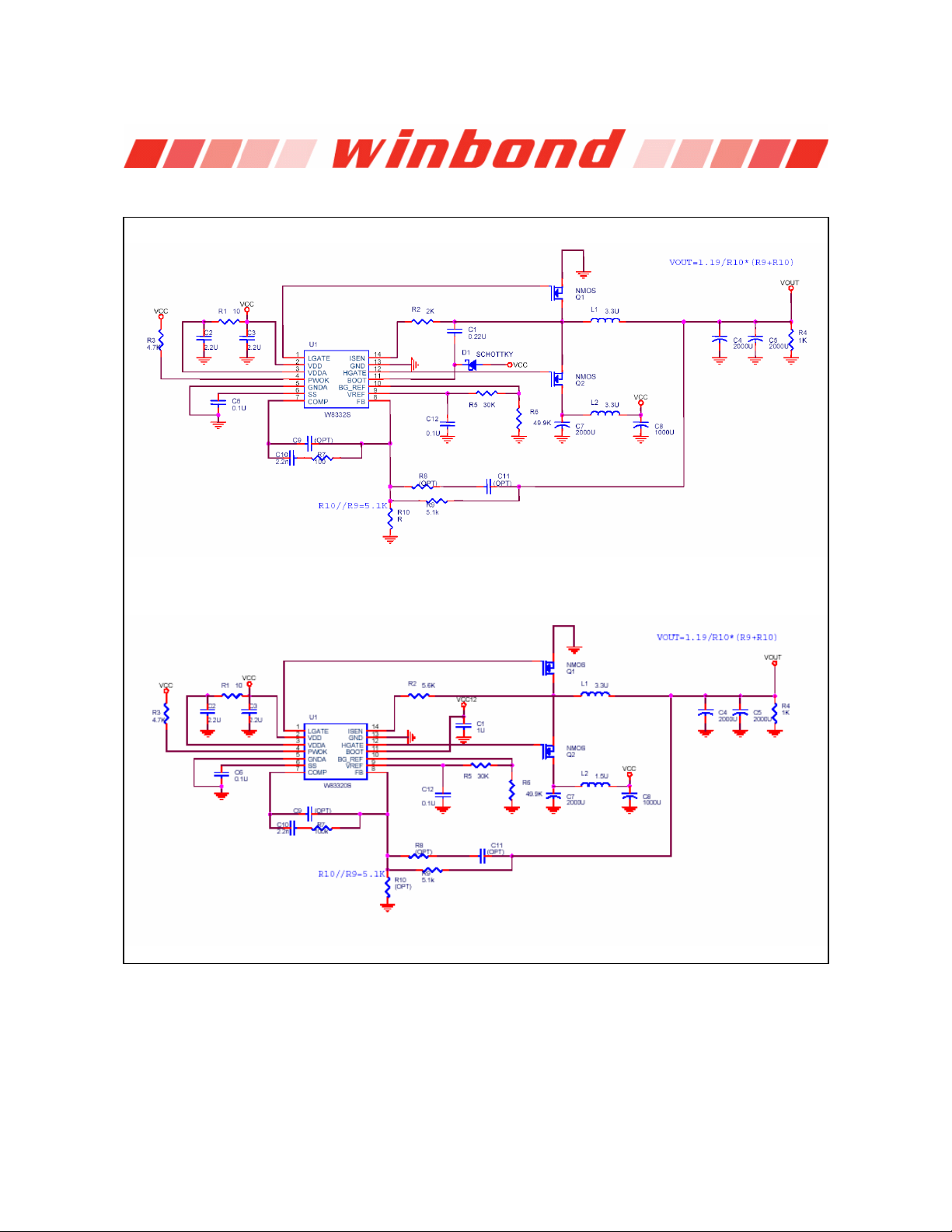
7. APPLICATION CIRCUIT
W83320S/W83320G
Publication Release Date: January 10, 2006
- 9 - Revision 0.51
Page 10
W83320S/W83320G
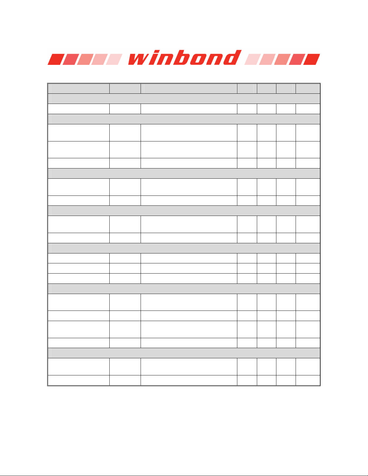
8. ELECTRICAL CHARACTERISTICS
PARAMETER SYMBOL TEST CONDITIONS MIN TYP MAX UNITS
VCC SUPPLY CURRENT
Nominal Supply I
CC
POWER-ON RESET
Rising VDD
Threshold
Falling VDD
Threshold
REFIN Enable - 0.27 - V
OSCILLATOR
Free Running
Frequency
Ramp Amplitude ΔV
REFERENCE
Reference Voltage
Tolerance
V
REF
Reference Voltage - 1.19 - V
EN=VCC; UGATE and LGATE Open - 3 - mA
- 4.3 - V
- 3.7 - V
R
OSC
=49.6K 160 200 240 kHz
SET
R
=49.6K - 1.5 - V
SET
-1.5 - 1.5 %
P-P
ERROR AMPLIFIER
DC Gain - 80 - dB
Gain-Bandwidth - 5 - MHz
Slew Rate - 4 - V/
µS
GATE DRIVERS
High-side Gate
Source
High-side Gate Sink I
Low-side Gate
Source
Low-side Gate Sink I
I
HGATE-SRC
HGATE-SNK
I
LGATE-SRC
LGATE-SNK
V
=12V,V
BOOT
V
=12V,V
BOOT
VCC=5V, V
VCC=5V, V
=6V 250 - - mA
UGATE
=6V 600 - - mA
UGATE
=2.5V 250 - - mA
LGATE
=2.5V 300 - - mA
LGATE
PROTECTION
ISEN Current
Source
Soft-Start Current I
I
SEN
SS
64 72 80 µA
10 12 14 µA
- 10 -
Page 11
W83320S/W83320G
K
K
9. TYPICAL PERFORMANCE CHARACTERISTICS
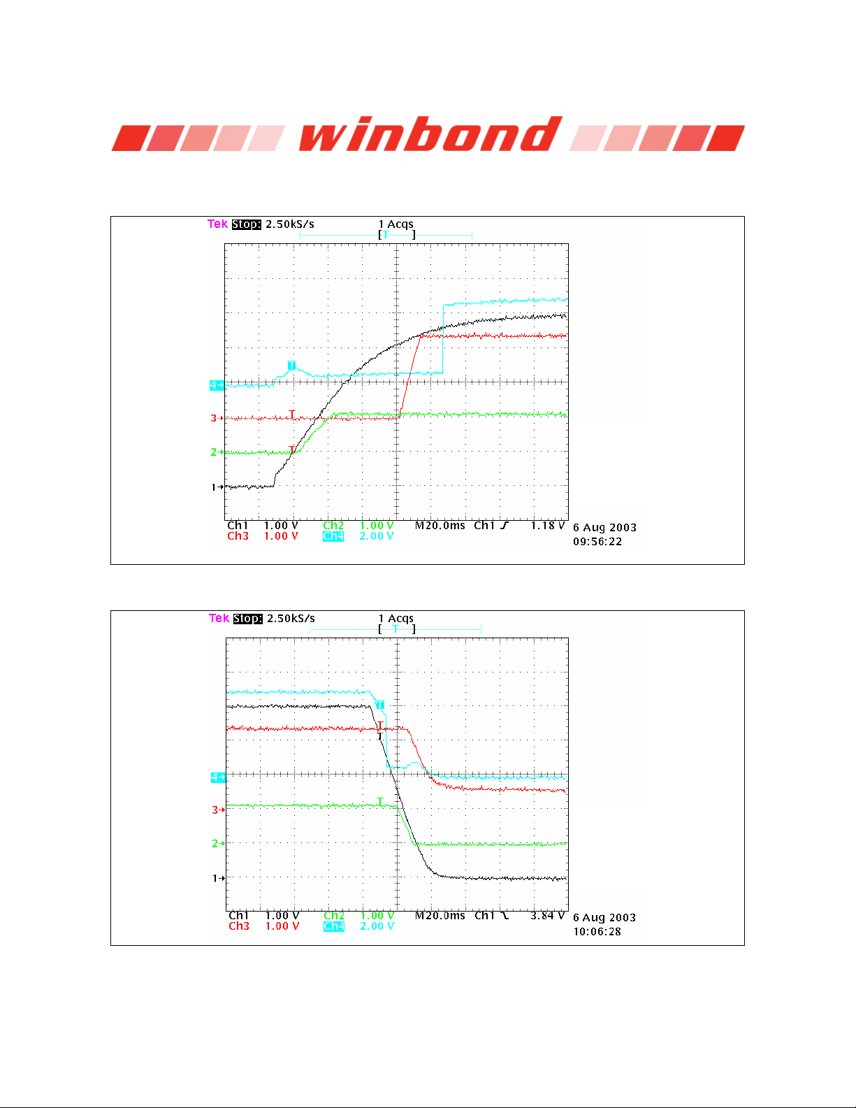
- Power start up with condition: no loading; CSS=0.1uF; VCC=5V; VOUT=2.5V; f = 200 KHz.
Ch1: V
Ch2: V
Ch3: V
CC
REF
OUT
Ch4: PWRO
- Power shut down with condition: no loading; CSS=0.1uF; VCC=5V; VOUT=2.5V; f = 200 KHz.
Ch1: V
Ch2: V
Ch3: V
CC
REF
OUT
Ch4: PWRO
Publication Release Date: January 10, 2006
- 11 - Revision 0.51
Page 12
W83320S/W83320G
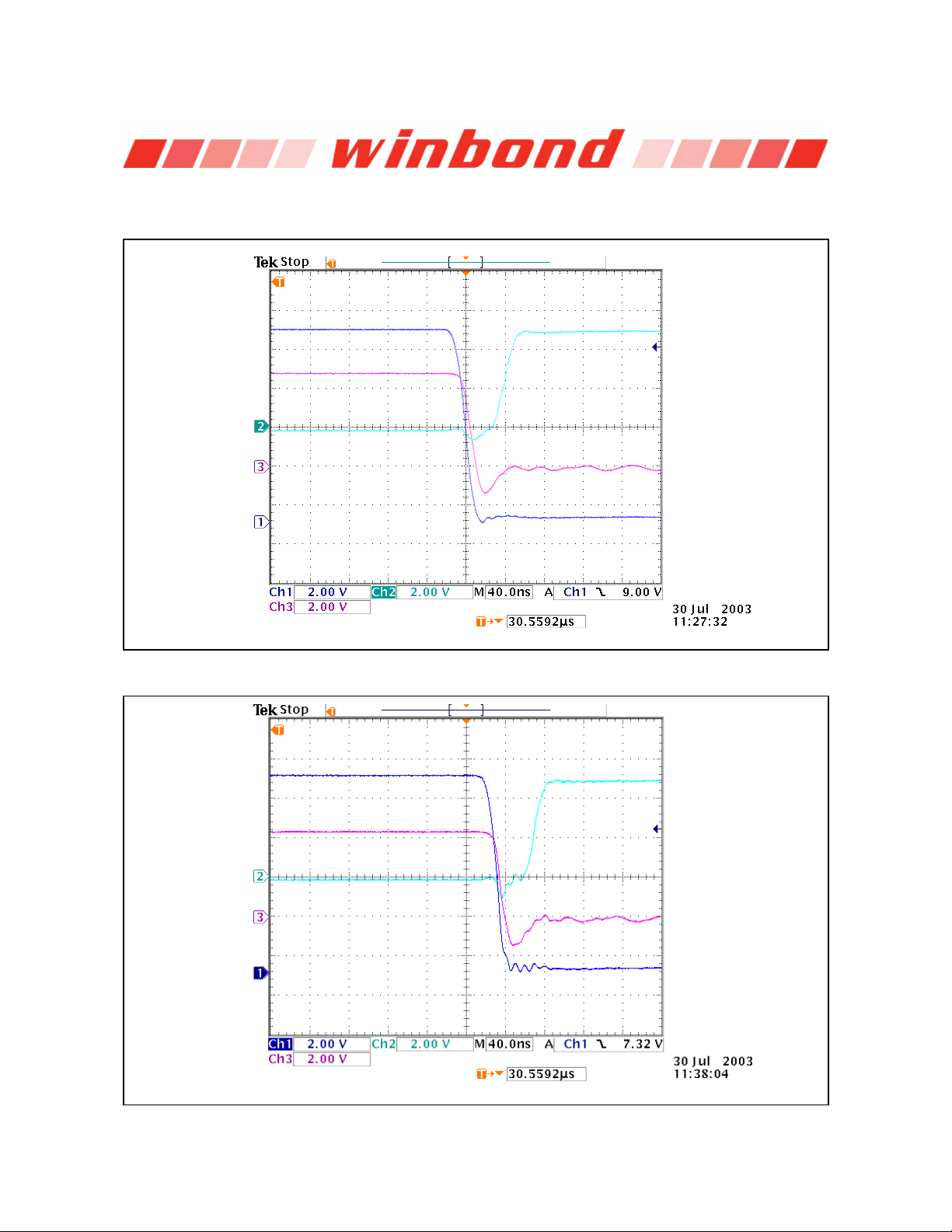
- High gate switch off with condition: no loading; CSS=0.1uF; VCC=5V; VOUT=2.5V; f = 200
KHz.
Ch1: UGATE
Ch2: LGATE
Ch3: Phase
- High gate switch off with condition: 2Amp loading; CSS=0.1uF; VCC=5V; VOUT=2.5V; f = 200
KHz.
Ch1: UGATE
Ch2: LGATE
Ch3: Phase
- 12 -
Page 13
W83320S/W83320G
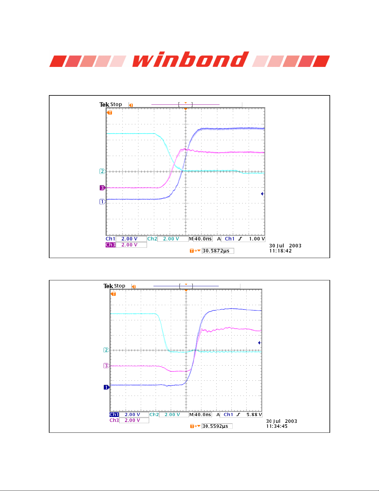
- High gate switch on with condition: no loading; CSS=0.1uF; VCC=5V; VOUT=2.5V; f = 200
KHz.
Ch1: UGATE
Ch2: LGATE
Ch3: Phase
- High gate switch on with condition: no loading; CSS=0.1uF; VCC=5V; VOUT=2.5V; f = 200
KHz.
Ch1: UGATE
Ch2: LGATE
Ch3: Phase
Publication Release Date: January 10, 2006
- 13 - Revision 0.51
Page 14
W83320S/W83320G
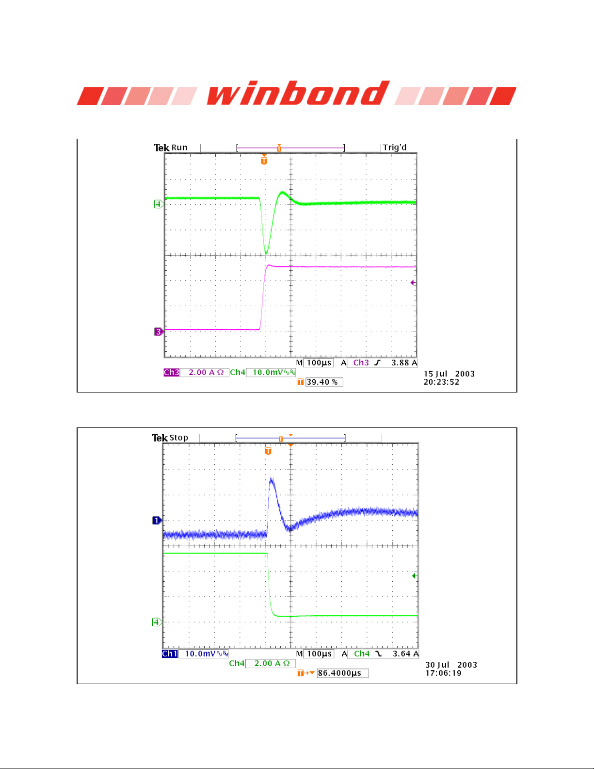
- Load transient response with condition: 0.5Amp to 5.5Amp; CSS=0.1uF; VIN=5V; VOUT=2.5V;
f = 200 KHz.
Ch1: I
Ch4: V
- Load transient response with condition: 5.5Amp to 0.5Amp; CSS=0.1uF; VIN=5V; VOUT=2.5V;
f = 200 KHz.
OUT
OUT
- 14 -
Ch1: V
Ch4: I
OUT
OUT
Page 15
W83320S/W83320G
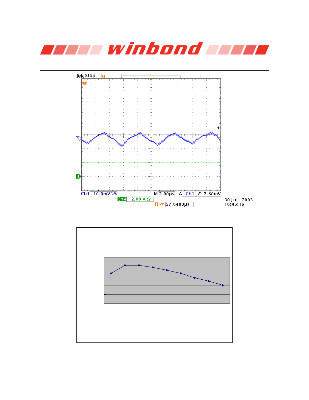
- Output load transient response with condition: IOUT=2Amp; CSS=0.1uF; VIN=5V; VOUT=2.5V;
f = 200 KHz.
- Regulation efficiency with various loading
Efficiency(Vin=5V,Vout=2.5V)
96
94.34
94
92
92.59
90
88
Efficiency(%)
86
94.34
93.9
93.28
92.59
91.62
90.9
90
Ch1: V
Ch4: I
OUT
OUT
123456789
Output current(A)
Publication Release Date: January 10, 2006
- 15 - Revision 0.51
Page 16
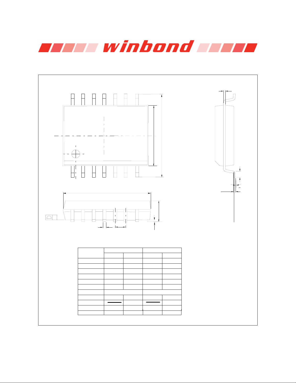
10. PACKAGE DIMENSION OUTLINE
14L SOP (150mil)
W83320S/W83320G
Y
SEATING PLANE
14
1
8
E
H
E
c
L
7
D
A
e
b
A1
0.25
O
GAUGE PLANE
Control demensions are in milmeters .
SYMBOL
A
A1
b
c
E
D
e
H
E
Y
L
θ
DIMENSION IN MM
MIN.
1.35
0.10
0.33
0.19
3.80
8.55
1.27 BSC
5.80
0.40
08
MAX.
1.75
0.25
0.51
0.25
4.00
8.75
6.20
0.10
1.27
DIMENSION IN INCH
MIN.
0.053
0.004
0.013
0.008
0.150
0.337
0.050 BSC
0.228
0.016
0
MAX.
0.069
0.010
0.020
0.010
0.157
0.344
0.244
0.004
0.050
8
- 16 -
Page 17
11. ORDERING INSTRUCTION
PART NO. PACKAGE REMARKS
W83320S/W83320G
W83320S 14-pin SOP
W83320G 14-pin SOP Operation - Commercial 0~70℃,Pb-free package
Operation - Commercial 0~70℃
12. HOW TO READ THE TOP MARKING
W83320S
2322906Z-N
323GA
Left Line: Winbond Logo
st
1
Line: Part No – W83320S,W83320G(Pb-free part no)
nd
2
Line: IC Tracking Code
rd
3
Line: Manufacturing Date Code (X XX) + Assembly Code (X) + IC Version (X)
W83320G
2322906Z-N
323GA
Publication Release Date: January 10, 2006
- 17 - Revision 0.51
Page 18

W83320S/W83320G
Please note that all data and specifications are subject to change without notice. All the trade
marks of products and companies mentioned in this data sheet belong to their respective
owners.
Important Notice
Winbond products are not designed, intended, authorized or warranted for use as components
in systems or equipment intended for surgical implantation, atomic energy control
instruments, airplane or spaceship instruments, transportation instruments, traffic signal
instruments, combustion control instruments, or for other applications intended to support or
sustain life. Further more, Winbond products are not intended for applications wherein failure
of Winbond products could result or lead to a situation wherein personal injury, death or
severe property or environmental damage could occur.
Winbond customers using or selling these products for use in such applications do so at their
own risk and agree to fully indemnify Winbond for any damages resulting from such improper
use or sales.
- 18 -
Page 19

 Loading...