

Page 1

Advanced ACPI Controller
W83303AD/W83303AG
Winbond
W83303AD/W83303AG
Page 2
W83303AD/W83303AG
W83303AD/AG
Data Sheet Revision History
Pages Dates Version
1 N.A. N.A.
2 N.A. 10/25/04 0.5 N.A. First published preliminary version.
3 N.A. 12/20/04 0.51 N.A.
4 12,13,14 1/09/06 0.52 N.A. Modified the application circuit.
5
6
7
8
Please note that all data and specifications are subject to change without notice. All the trademarks of
products and companies mentioned in this data sheet belong to their respective owners.
Version
on Web
Main Contents
All of the versions before 0.50 are for internal
use.
Add part no of W8303AG with Pb-free
package.
LIFE SUPPORT APPLICATIONS
These products are not designed for use in life support appliances, devices, or
systems where malfunction of these products can reasonably be expected to result in
personal injury. Winbond customers using or selling these products for use in such
applications do so at their own risk and agree to fully indemnify Winbond for any
damages resulting from such improper use or sales.
Page 3

W83303AD/W83303AG
1. GENERAL FUNCTION DESCRIPTION
y Provides Voltages
− 5V Active/Sleep (5VDUAL)
/5V
− Programmable 5V
− 3.3V Active/Sleep (3.3VDUAL)
− Programmable Dual-Channels RAM Active/Sleep (V
− Auto-detective 2.6V
− Two Programmable Linear Regulators and one Linear Regulator Ranging 1.2V~5.00V for
Over-Clocking Application
− 1.2V VCCVID for Intel® P4 CPU or FSB_VTT for Grandsdale
− 1.5V VPCI Voltage
y Supports VRGOOD signal for Intel® P4 CPU Power Good Control
y Supports RSMRST# Signal Control
y Provides Signals for ATX Power Supply PS_ON# Control
y I2C Interface
y Selectable I2C Address
y Internal Charge Pump Support Up to 9.5VSB
y Drive All N-Channel MOSFET
y Soft Start
y Under-Voltage Monitoring for 3VDUAL, VPCI and VRAM Channels
DL
/5VCC for USB Devices(5VUSB)
STR
STR
/1.8V
for DDR/DDRII Voltage
STR
) for DDR
STR
Publication Release Date: Jan. 9, 2006
- 1 - Revision 0.52
Page 4
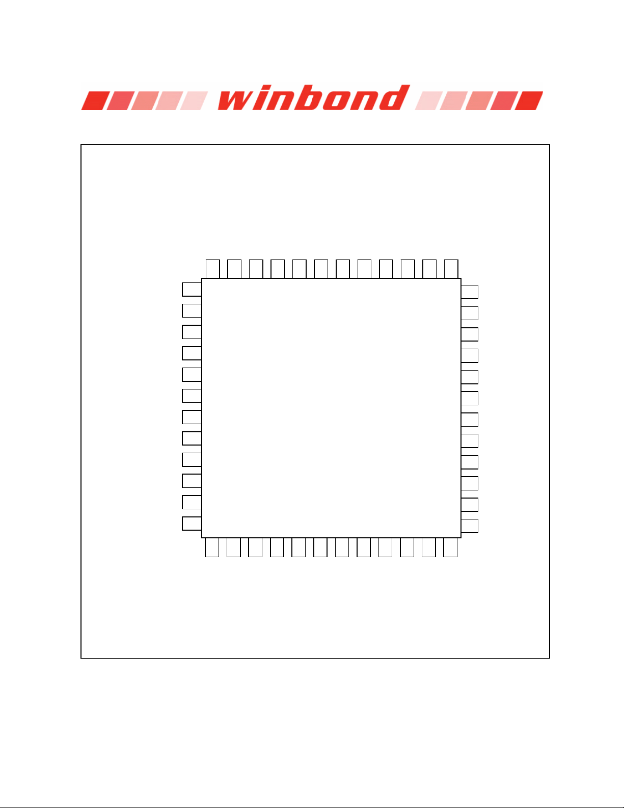
2. W83303AD/AG PIN-OUT
LR1_DRV
VCC
36 35 34 33 32 31 30 29 28 27 26 25
VPCI_SEN
VPCI_DRV
AGND
CHRPMP
C2
W83303AD/W83303AG
C1
5VSB
1.2V_DRV
1.2V_SEN
VRGOOD
LR1_SEN
LR2_DRV
LR2_SEN
DDRDET#
FAULT#
PS_IN#
PW_BUT#
PS_OUT#
DGND
PWR_OK
A0
D5VSB
37
38
39
RSMRST#
PWM_MODE
LR3_SEN
LR3_DR V
AGND
40
41
42
43
44
45
46
47
48
1 2 3 4 5 6 7 8 9 10 11 12
S3#
W83303AD/AG
S5#
I2C_CLK
I2C_DATA
5VUSB
5VSBDRV
AGND
24
VRAM_DRV1
23
I_SEN1
22
VRAM_SEN
21
VRAM_DRV2
20
I_SEN2
19
5VSB
18
ISET
17
SS
16
VCC3
15
3.3VSB_DRV
14
3.3V_SEN
13
3V/5VDRV
- 2 -
Page 5
W83303AD/W83303AG
A
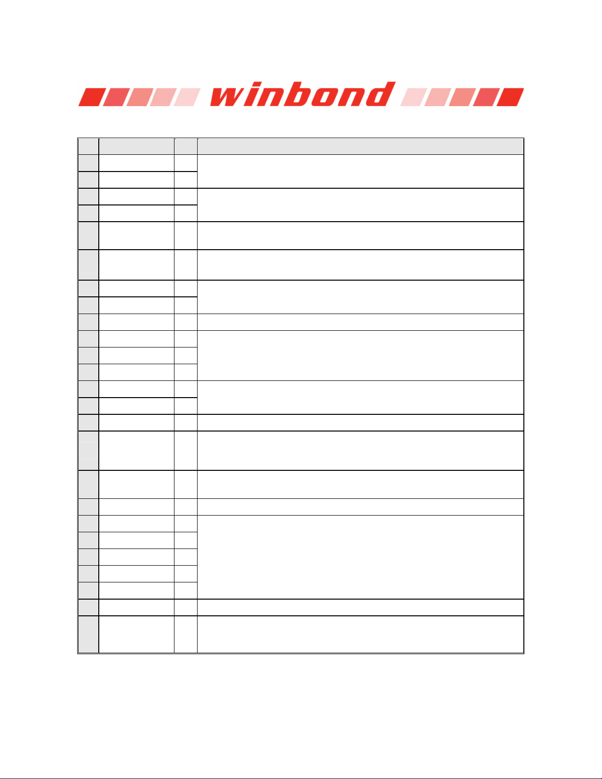
3. PIN DESCRIPTIONS
NO NAME I/O FUNCTION DESCRIPTION
1
2 S5# I
S3# I
SYSTEM ACPI CONTROL SIGNALS
3 I2C_DATA I/O
4 I2C_CLK I
5 RSMRST# OD
6 PWM_MODE I
7 LR3_SEN I
8 LR3_DRV O
9 AGND P Power ground
10 5VUSB O
11 5VSBDRV O
12 5VDRV O
13 3.3V_SEN I
14 3.3VSB_DRV O
15 VCC3 P Power 3.3Vcc
16 SS I
17 I
SET
I2C Interface, and the default ID value are defined as 5CH (0101 110X) as
well as 5EH (0101 111X), and X is used to control read/write.
A signal to indicate 3VDUAL power status. The signal will be issued after
82ms delay when the level of 3VDUAL higher than 2.8V
0=Internal RAM for Linear Mode;
1= external RAM for PWM Mode
Linear Regulators ranging form 1.2V to 5V and can be adjusted by
external resistors
Power switch for USB devises provides a programmable Voltage
(5VDUAL/5VSTR/ 5VCC) for USB devices. It can be set by register CR00
3.3VDUAL Voltage regulator
Soft-Start pin. Attach a capacitor to this pin to determine the soft-start rate;
and the slew-rate of SS is set by adjust the capacity of the external
capacitor.
ttached a specific external resistor to determine the internal reference
I
current.
18 5VSB P Power Pin
19 I_SEN2 I
20 VRAM_DRV2 O
21 VRAM_SEN I
22 I_SEN1 I
23 VRAM_DRV1 O
24 AGND P Power ground
25 VRGOOD OD
2 channels of V
design to balance the current on the channels. In which I_SEN1 & I_SEN2
pins should be connected together to 5VSB or 3VDUAL if only one
channel used. The DDR or DDRII determine by DDRDET#. If DDRDET#
=0 VRAM=DDR(2.6V) ; DDRDET#=1 VRAM=DDRII(1.8V).
The signal is applied for the Intel® Northwood CPU using; it’s a signal to
declare the CPU VID status.
output for DDR or DDRII with internal current sharing
STR
Publication Release Date: Jan. 9, 2006
- 3 - Revision 0.52
Page 6
W83303AD/W83303AG
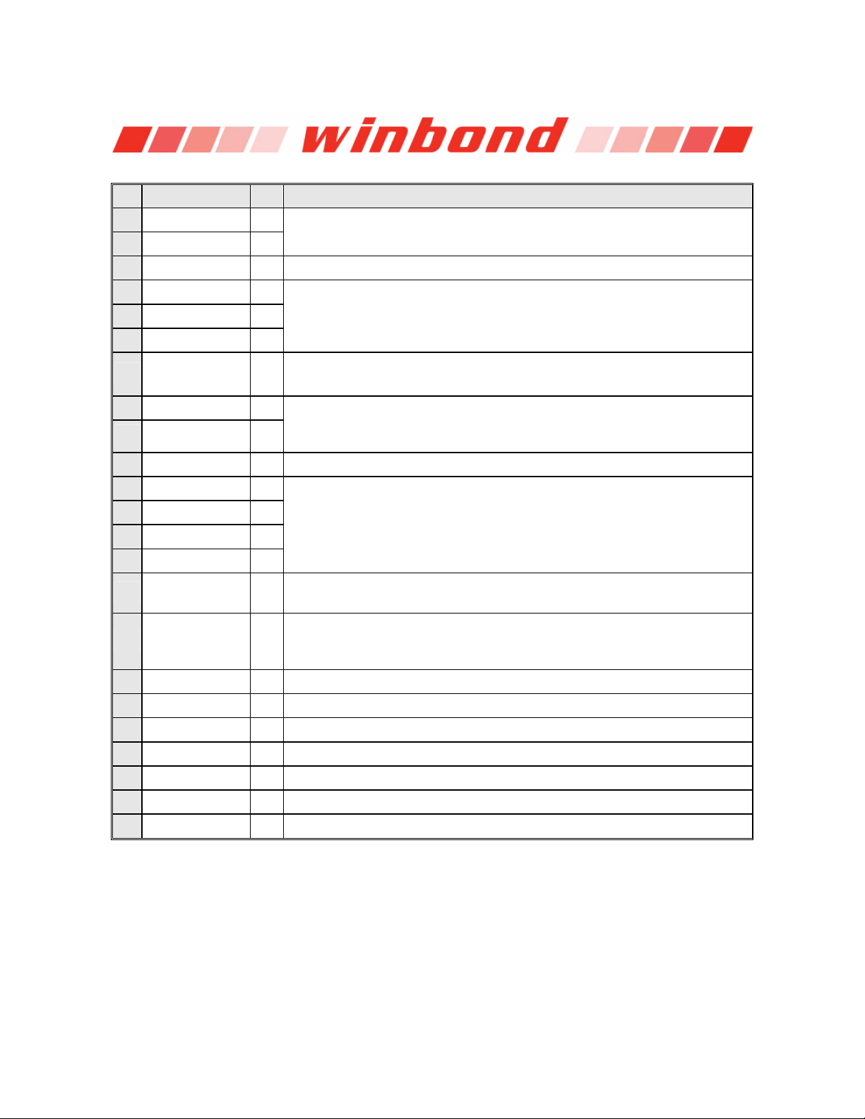
Pin Descriptions, continued
NO NAME I/O FUNCTION DESCRIPTION
26 1.2V_SEN I
27 1.2V_DRV O
28 5VSB P Power Pin
29 C1 I
30 C2 I
31 CHRPMP P
1.2V
Charge pump pins. It supports 10mA driving current and insures output
voltage 9V or above.
voltage regulator for Intel® P4 CPU application.
CC
32 AGND P
33 VPCI_DRV O
34 VPCI_SEN I
35 VCC P Power pin
36 LR1_DRV O
37 LR1_SEN I
38 LR2_DRV O
39 LR2_SEN I
40 DDRDET# I
41 FAULT# I
42 PS_IN# Power on signal. Low active.
43 PW_BUT# I System PW_BUT for power sequence monitoring.
44 PS_OUT# O Pin to control ATX power supply.
45 DGND P Power ground.
Power pin
1.5V Voltage Regulator for PCI Express. If this power plane won’t be
used, the VPCI_SEN must be connected to 3VDUAL to avoid the fault
trigger of LUV event.
Linear Regulators ranging form 1.2V to 5V and can be adjusted by
external resistors
A signal to indicate type of DDRRAM that plugged- in; low means 2.6V for
DDR and high means 1.8V for DDRII.
Fault event be monitored; the chip shut the ATX power supply down
directly by control the PS_ON# signal as long as the fault events are
triggered.
46 PWR_OK I Power good input signal of ATX power supply.
47 A0 I I2C address selecting pin.
48 D5VSB P Power pin.
*VRGOOD & TYPEDET# can endure 0-12V level voltage.
- 4 -
Page 7
W83303AD/W83303AG
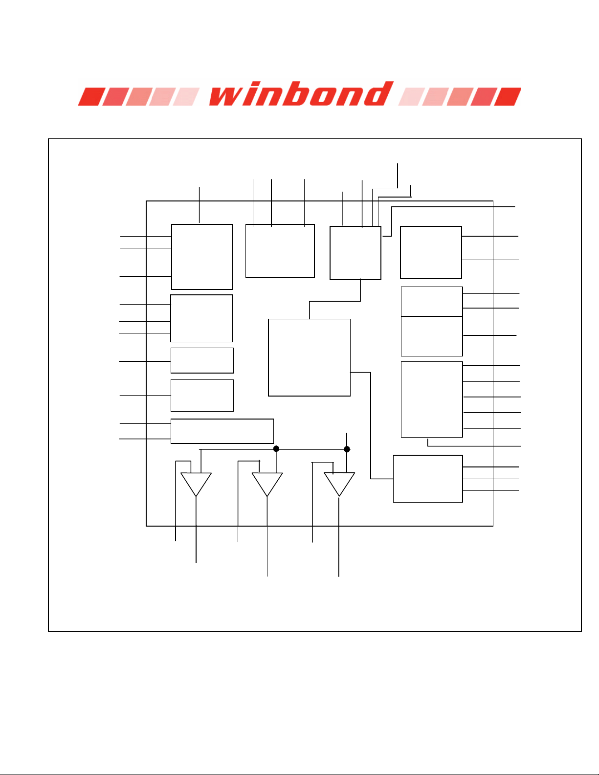
4. INTERNAL BLOCK DIAGRAM
C1 CHRPMP S5#
PS_IN#
FAULT#
PS_OUT#
PW_BUT#
Reset
Integrated
Circuit
C2
Charge
Pump
S3#
Control
Circuit
PWR_OK
DDRDET#
RSMRST#
3.3V_SEN
3.3VDL
3.3V_DRV
VRGOOD
1.2V_DRV
1.2V_SEN
ISET
VPCI_DRV
VPCI_SEN
SS
LR_SEN1
LR_DRV1
1.2V
VCCVID
Soft Start
Reference
Current
PCI express 1.5V
LR_SEN2
LR_DRV2
Control
Register
LR_SEN3
1.20V
LR_DRV3
5VDL
5VUSB
VRAM
I2C
5VDRV
5VSBDRV
5VUSB
VRAM_DRV1
I_SEN11
VRAM_SEN1
VRAM_DRV2
I_SEN2
EXT_RAM
I2C_CLK
I2C_DATA
A0
Publication Release Date: Jan. 9, 2006
- 5 - Revision 0.52
Page 8
W83303AD/W83303AG
5. I2C COMMUNICATION PROTOCOL
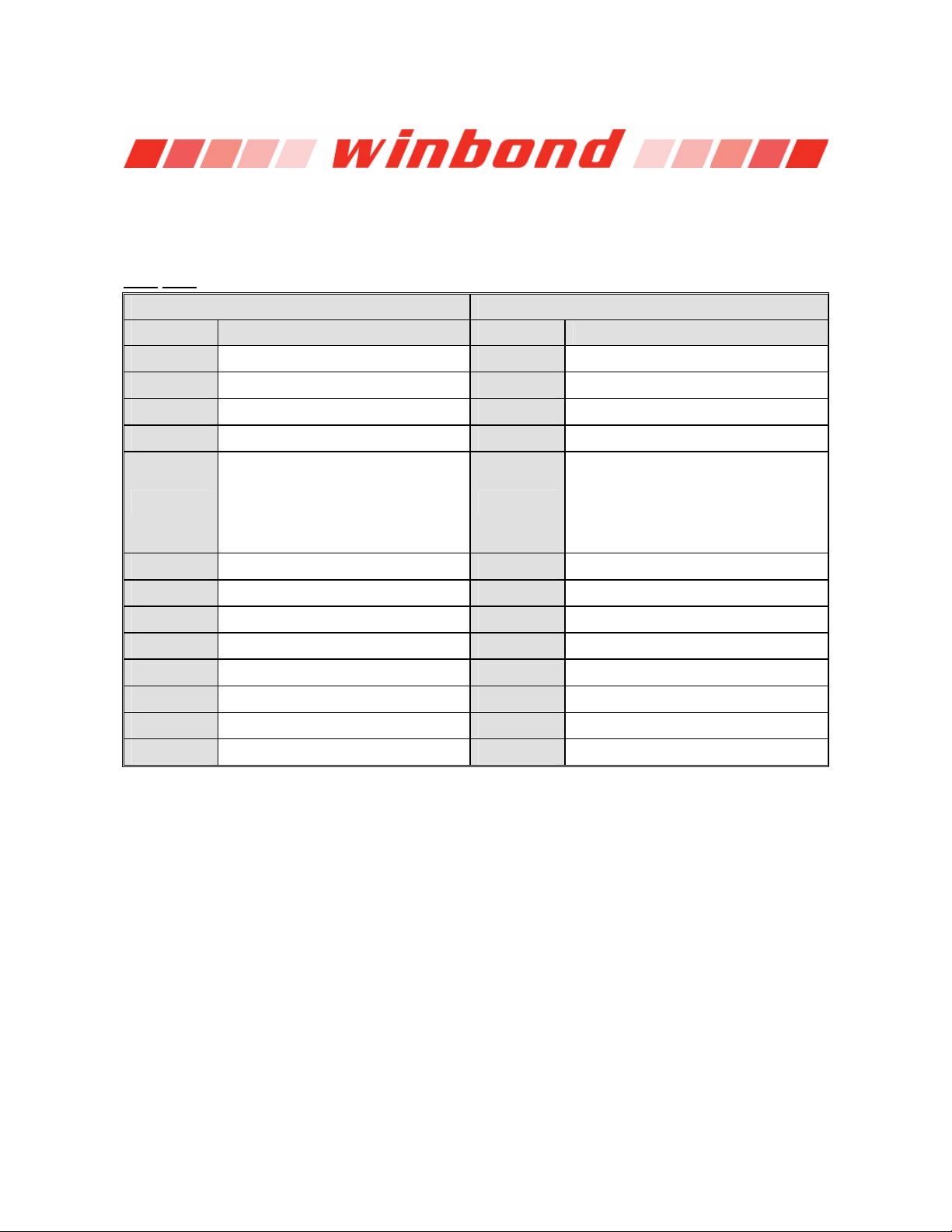
The W83303AD/AG serial protocol accepts byte write, byte read operation from the controller. For the
byte write and byte read operations, the system controller can access individual indexed bytes. The
byte write and byte read protocol is outlined in following table. Besides, the slave receiver address is
0101 1110(5Eh).
BYTE WRITE BYTE READ
BIT DESCRIPTION BIT DESCRIPTION
1
2:8
9
10
Start
Slave address – 7 bits
Write
Acknowledge from Slave
1
2:8
9
10
Start
Slave address – 7 bits
Write
Acknowledge from slave
11:18
19
20:27
28
29
Command Code – 8 bits
‘1xxxxxx’ stands for byte
operation bit[6:0] of the command
code represents the offset of the
byte to be accessed
Acknowledge from slave
Data byte – 8 bits
Acknowledge from slave
Stop
11:18
19
20
21:27
28
29
30:37
38
39
Command Code – 8 bits
‘1xxxxxx’ stands for byte operation
bit[6:0] of the command code
represents the offset of the byte to
be accessed
Acknowledge from slave
Repeat start
Slave address – 7bits
Read
Acknowledge from slave
Data byte from slave – 8bits
Not Acknowledge
Stop
- 6 -
Page 9
W83303AD/W83303AG
6. REGISTER DESCRIPTION
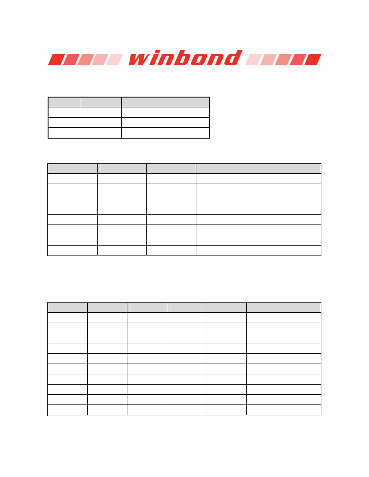
6.1 CR00 (5VUSB Setting Register, Default 0x00h, Read/Write)
BIT1 BIT0 SUPPORT ACPI STATE
0 1 S0, S3
0 0 S0, S3, S5
1 1 S0
6.2 CR01 (VPCI Voltage Setting Register, Default 0x00h, Read/Write)
Bit7~3: Reserved
BIT2 BIT1 BIT0 VAGP OUTPUT
0 0 0 1.50V
0 0 1 1.55V
0 1 0 1.60V
0 1 1 1.65V
1 0 0 1.70V
1 0 1 1.80V
1 1 0 1.90V
1 1 1 2.00V
6.3 CR02 (VRAM Voltage Setting Register, Default x000 0000 b, Read/Write)
Bit7 is reserved for signal DDRDET# Setting (Dynamic detect)
DDRDET#=H bit7=1 DDRII type, DDRDET#=L bit7=0 DDRI type.
Bit3,2, 1 and 0 are applied for DDRRAM output adjusting.
BIT7 BIT3 BIT2 BIT1 BIT0 VRAM OUTPUT
0 0 0 0 0 2.60V
0 0 0 0 1 2.50V
0 0 0 1 0 2.55V
0 0 0 1 1 2.65V
0 0 1 0 0 2.70V
0 0 1 0 1 2.80V
0 0 1 1 0 2.90V
0 0 1 1 1 3.00V
0 1 0 0 0 3.10V
0 1 0 0 1 3.20V
Publication Release Date: Jan. 9, 2006
- 7 - Revision 0.52
Page 10
W83303AD/W83303AG
BIT7 BIT3 BIT2 BIT1 BIT0 VRAM OUTPUT
1 0 0 0 1 1.75V
1 0 0 1 0 1.85V
1 0 0 1 1 1.90V
1 0 1 0 0 1.95V
1 0 1 0 1 2.00V
1 0 1 1 0 2.05V
1 0 1 1 1 2.10V
1 1 0 0 0 2.20V
1 1 0 0 1 2.30V
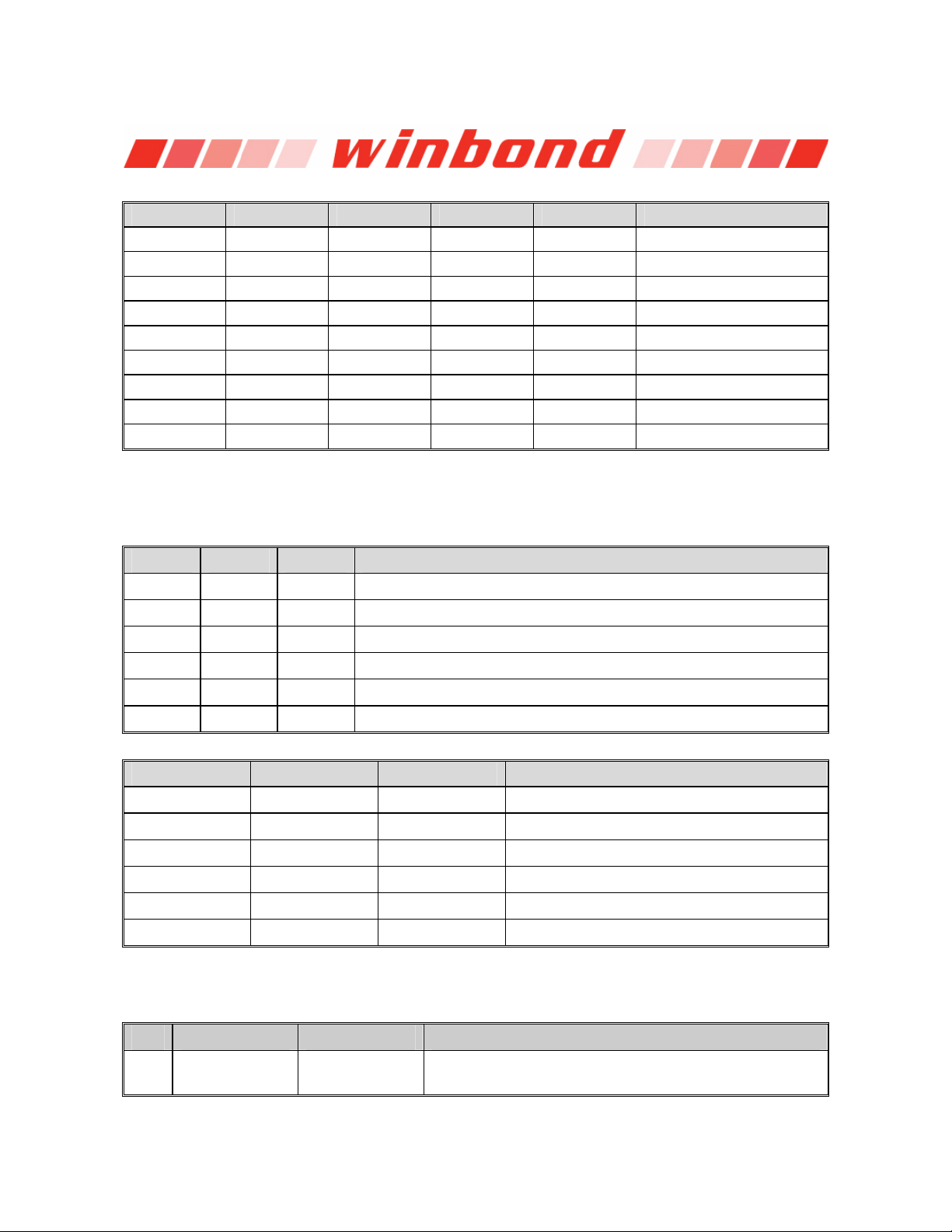
6.4 CR03 (Linear Regulator 1,2 Voltage Setting Register, Default 0x00h, Read/Write)
VLR1: Bit2, 1 and 0 are applied for output voltage adjusting.
BIT2 BIT1 BIT0 PERCENTAGE OF VOLTAGE INCREASE
0 0 0 +0%
0 0 1 +2%
0 1 0 +4%
0 1 1 +8%
1 0 0 +12%
1 0 1 +16%
VLR2 : Bit2, 1 and 0 are applied for output voltage adjusting.
BIT6 BIT5 BIT4 PERCENTAGE OF VOLTAGE INCREASE
0 0 0 +0%
0 0 1 +2%
0 1 0 +4%
0 1 1 +8%
1 0 0 +12%
1 0 1 +16%
6.5 CR04 Chip ID
Power on default [7:0] = 1010,0001 b
Bit Name Read/Write Description
7-0 CHIPID[7:0] Read Only
Winbond Chip ID number. Read this register will return
0xa1h for W83303AD/AG.
- 8 -
Page 11
W83303AD/W83303AG
6.6 CR05 (Linear-Under-Voltage Setting Register) default 0x07
Bit0, 1 and 2 are applied for Linear-Under-Voltage Protection functions enable/di sable.
BIT0
BIT1
BIT2
BIT3
BIT4
BIT5
1/0 Enable/disable VPCI LUV, default value=1
1/0 Enable/disable VRAM LUV, default value=1
1/0 Enable/disable Dual3.3V LUV, default value=1
1/0
1/0
1/0
Enable/disable RSRMST# restart as release latching fault or LUV event
Default value = 0 (disable)
Enable/disable Power Button release latching fault event.
Default value = 0 (disable)
Enable/disable Power Button release latching LUV event.
Default value = 0 (disable)
6.7 CR06 Version ID
Power on default [7:0] = 0000,0000 b
Bit Name Read/Write Description
7-0 CHIPID[7:0] Read Only
Winbond Version ID number. Read this register will
return 0x00h for W83303AD/AG.
Publication Release Date: Jan. 9, 2006
- 9 - Revision 0.52
Page 12
W83303AD/W83303AG
7. ELECTRICAL SPECIFICATION
7.1 AC CHARACTERISTICS
Vcc=5V ± 5 %, TA = 0°C to +70°C
PARAMETER SYMBOL MIN TYP MAX UNITS TEST CONDITIONS
VPCI Linear Regulator
Nominal Output Voltage 1.50 V CR01(bit2~0)=000
Regulation 4 %
Under-Voltage Falling
Threshold
VPCI_DRV Output Voltage 8 V
Vref Voltage Reference
Nominal Output Voltage 1.152 1.2 1.248 Iload < 1mA
1.2V Linear Regulator
Nominal Output Voltage 1.152 1.2 1.248 V
VRGood delay 2 mS
VRAM Regulator
Nominal Output Voltage 2.60 V CR02(bit7)=0
Nominal Output Voltage 1.80 V CR02(bit7)=1
Regulation 4 %
Under-Voltage Falling
Threshold
MAX VRAM_DRV Output
Voltage
Increase percentage of Linear Regulator _1,2 output voltage (%)
Nominal Output Voltage 0 %
70 %
I(VPCI_DRV) <
0.3mA
After
1.2V_SEN>1.1V
70 %
8 V
I(VRAM_DRV) <
0.3mA
Nominal Output Voltage 2 %
Nominal Output Voltage 4 %
Nominal Output Voltage 8 %
Nominal Output Voltage 12 %
Nominal Output Voltage 16 %
Soft Start Source current
Soft start current 20 uA
- 10 -
Page 13
AC CHARACTERISTICS, continued
5VDUAL Switch Controller
5VDRV Output High
Voltage
W83303AD/W83303AG
9 Cap Loading
5VSBDRV Output High
Voltage
5VUSB Output High
Voltage
5VUSB SS Sourcing
Current
3.3VDUAL
Under-Voltage Falling
Threshold
MAX 3VSBDRV Output
Voltage
Charge Pump
Charge Pump Frequency 200 KHz
Charge Pump Voltage 9.5
9 Cap Loading
9 Cap Loading
2.5 uA @ Soft-start
70 %
9 V
I(3VSBDRV) <
0.3mA
Publication Release Date: Jan. 9, 2006
- 11 - Revision 0.52
Page 14
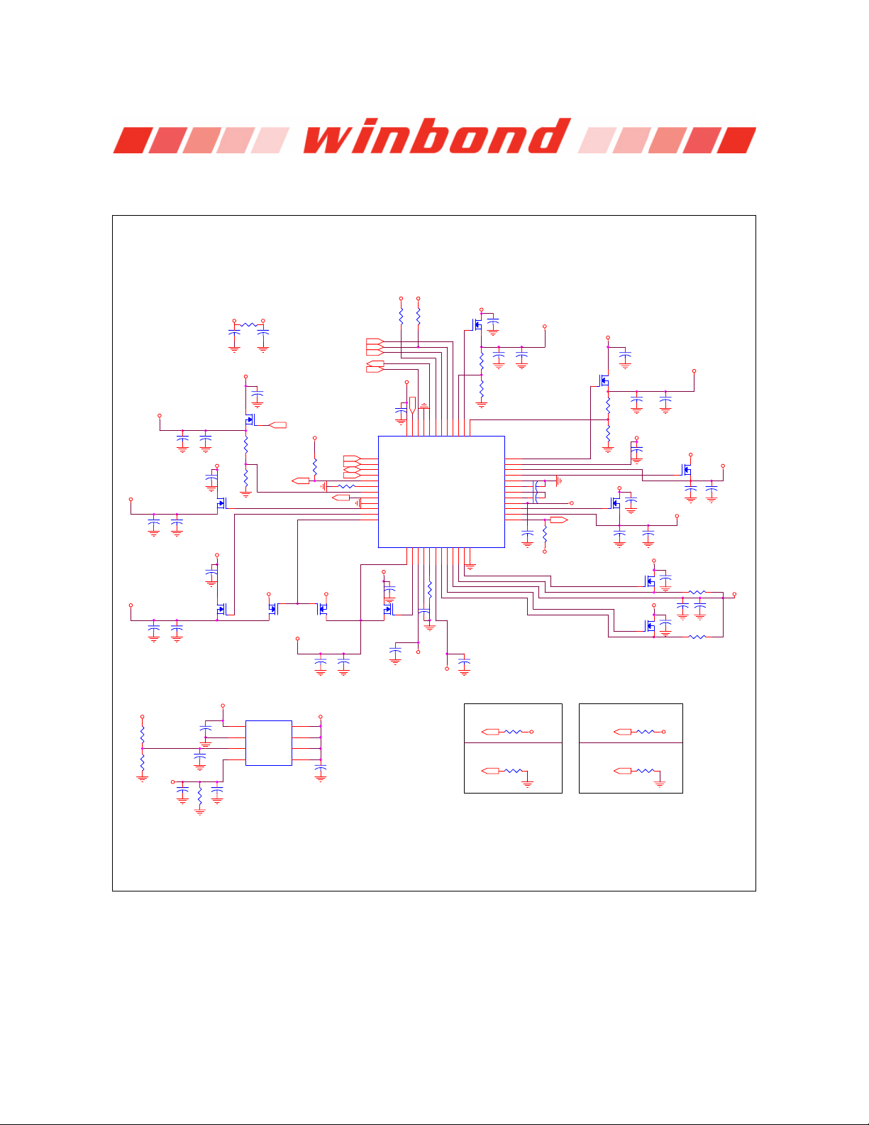
8. APPLICATION CIRCUIT
8.1 Linear Mode
5VSB
W5VSB
R3
5
VLR3=1.2X(R8+R10)/ R10
5VUSB
C20
1000U
5VDUAL
C32
1000U
C11
1000U
C21
1000U
MOSFET N
C33
1000U
5VDUAL
C14
10U
Q5MOSFET N
C25
10U
Q8
C2
0.1U
DUAL/VSB/VSTR/VCC
C12
1000U
13
5VSB
13
Q3MOSFET N
R10
R
2
2
13
R8
R
MOSFET N
Q9
0.1U
C7
10U
2
RSMRST#
VCC5
C3
PS_OUT#(to ATX)
PWR_OK(from ATX)
LR3_DRV
5VSB
S3#
R9
S5#
4.7K
SDA
SCL
R11 1K
LR3_DRV
VCC3
MOSFET N
3VDUAL
C36
C35
1000U
1000U
DDRDET#
FAULT#
PS_IN#
Q10
1
2
3
4
5
6
7
8
9
10
11
12
Q11
R1
4.7K
C10
0.1U
S3#
S5#
I2C_DATA
I2C_CLK
RSMRST#
PWM_MODE
LR3_SEN
LR3_DRV
AGND
5VUSB
5VSBDRV
3V/5VDRV
5VSB
13
MOSFET N
C34
0.1U
5VSB
W5VSB
C27
10U
2
5VSB
R2
4.7K
A0
48
D5VSB
3.3V_SEN
13
VCC3
A0
3.3VSB_DRV
PWR_OK
C30
0.33U
DGND
PS_OUT#
W83303AD
ISETSSVCC3
R13
100K
PW_BUT#
5VSB
W5VSB
DUAL/VSB/VSTR/VCC
MOSFET N
3738394041424344454647
PS_IN#
FAULT#
LR2_SEN
LR2_DRV
DDRDET#
VRAM_DRV1
I_SEN1
VRAM_SEN
VRAM_DRV2
I_SEN2
2423222120191817161514
W83303AD/W83303AG
Q1
R4
R
R5
R
LR1_DRV
LR1_SEN
VPCI_SEN
VPCI_DRV
CHRPMP
1.2V_DRV
1.2V_SEN
VRGOOD
AGND
C37
0.1U
AGND
5VSB
VCC
C2
C1
C1
10U
C4
1000U
36
35
34
33
32
31
30
29
28
27
26
25
C22
0.1U
C15 0.1U
C18 0.1U
VLR2=1.2X(R4+R5)/ R5
C5
1000U
VRGOOD
R12
4.7K
VCC3/1.2V
DUAL/VSB/VSTR/VCC
Q6MOSFET N
W5VSB
Q2
MOSFET N
R6
R
R7
R
VCC3
1000U
MOSFET N
MOSFET N
VCC5
C23
C6
10U
Q7
Q12
C8
1000U
C13
0.1U
C19
10U
3VDUAL
3VDUAL
VLR1=1.2X(R6+R7)/ R7
C9
1000U
VCC3
Q4
1.2V
C24
1000U
C26
10U
C28
1000U
C31
10U
NMOS
C16
1000U
R14
4m
R15
4m
C29
1000U
VPCI
C17
1000U
VRAM
VRAM
VRAM
U1
1
R16
1K
R19
1K
VTT
C39
1n
R22
C41
1K
0.1U
C38
1500U
C42
1000U
VIN
2
GND
3 6
VREF VCNTL
4 5
VOUT VCNTL
W83310S-R2/DS
VCNTL
VCNTL
3VDUAL
8
7
C40
0.1U
A0=HIGH, I2C Add=0X5EH
R17 4.7K
A0 DDRDET#
A0=LOW, I2C Add=0X5CH
A0
5VSB
R20 1K
DDRDET#=HIGH, VRAM=1.8V
DDRDET#=LOW, VRAM=2.6V
DDRDET#
R18 4.7K
R21 1K
5VSB
- 12 -
Page 15
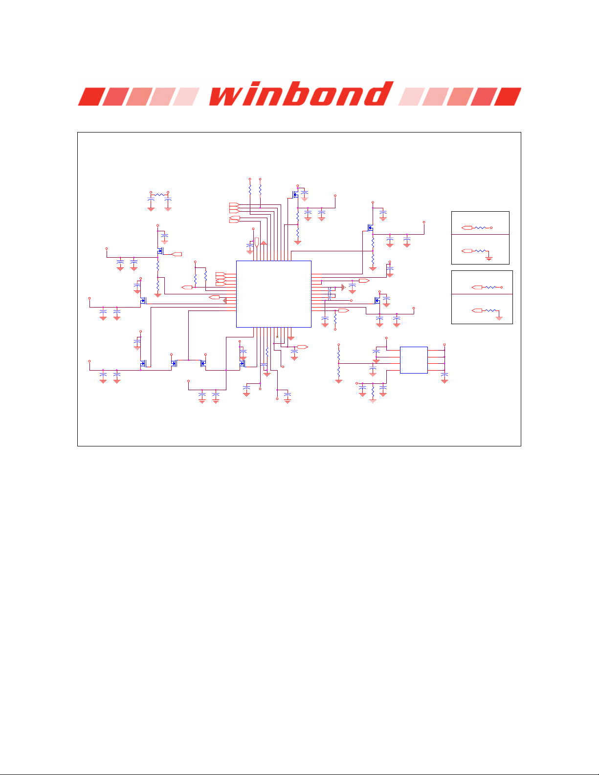
8.2 PWM Mode
W5VSB
R3
5VSB
5
C2
0.1U
DUAL/VSB/VSTR/VCC
13
Q3MOSFET N
2
R10
C12
5VUSB
5VDUAL
C19
1000U
C30
1000U
C11
1000U
C20
1000U
MOSFET N
C31
1000U
C14
10U
C24
10U
1000U
5VDUAL
Q4MOSFET N
5VSB
Q6
R
R13
R
RSMRST#
13
2
VCC5
13
MOSFET N
2
Q7
W83303AD/W83303AG
5VSB
5VSB
DUAL/VSB/VSTR/VCC
R2
R1
4.7K
4.7K
C3
0.1U
C7
10U
LR3_DRV
3VDUAL
R12
4.7K
1000U
5VSB
LR3_DRV
C36
DDRDET#
FAULT#
PS_IN#
PS_OUT#(to ATX)
PWR_OK(from ATX)
R11
S3#
4.7K
S5#
SDA
SCL
VCC3
MOSFET N
Q8
C37
1000U
1
2
3
4
5
6
7
8
9
10
11
12
Q9
C10
0.1U
S3#
S5#
I2C_DATA
I2C_CLK
RSMRST#
PWM_MODE
LR3_SEN
LR3_DRV
AGND
5VUSB
5VSBDRV
3V/5VDRV
5VSB
13
MOSFET N
C33
0.1U
W5VSB
C25
10U
A0
48
A0
D5VSB
PWR_OK
3.3VSB_DRV
3.3V_SEN
13
C28
2
VCC3
DGND
0.33U
MOSFET N
PS_OUT#
PW_BUT#
W83303AD
5VSB
ISETSSVCC3
R17
100K
W5VSB
PS_IN#
FAULT#
VRAM_DRV2
I_SEN2
3738394041424344454647
LR2_SEN
LR2_DRV
DDRDET#
VRAM_DRV1
I_SEN1
VRAM_SEN
2423222120191817161514
3VDUAL
Q1
R4
R
R6
R
LR1_DRV
LR1_SEN
VPCI_SEN
VPCI_DRV
CHRPMP
1.2V_DRV
1.2V_SEN
VRGOOD
AGND
C38
0.1U
AGND
C26
0.1U
VCC
5VSB
C1
10U
C2
C1
VRAM_REF
C4
1000U
36
35
34
33
32
31
30
29
28
27
26
25
C21
0.1U
C16 0.1U
C17 0.1U
VLR2=1.2X(R4+R6)/ R6
C5
1000U
R16
4.7K
VCC3/1.2V
VRAM
R18
1K
R19
1K
DUAL/VSB/VSTR/VCC
C15
0.1U
W5VSB
VRGOOD
VTT
C34
0.1U
R7
R
R9
R
VPCI_REF
VCC3
Q5MOSFET N
C29
1n
R20
1K
Q2
MOSFET N
VCC5
C22
1000U
VRAM
C27
1500U
C35
2000U
C6
10U
VLR1=1.2X(R7+R9)/ R9
C9
C8
1000U
1000U
C13
0.1U
C18
10U
1.2V
C23
1000U
U1
1
VIN
VCNTL
2
GND
VCNTL
3
VREF VCNTL
4 5
VOUT VCNTL
W83310S-R2/DS
3VDUAL
8
7
6
C32
0.1U
A0=HIGH, I2C Add=0X5EH
R5 4.7K
A0
A0=LOW, I2C Add=0X5CH
A0
DDRDET#=HIGH, VRAM=1.8V
DDRDET#
DDRDET#=LOW, VRAM=2.6V
DDRDET#
5VSB
R8 4.7KVLR3=1.2X(R10+R113)/ R13
R14 4.7K
R15 4.7K
5VSB
Publication Release Date: Jan. 9, 2006
- 13 - Revision 0.52
Page 16
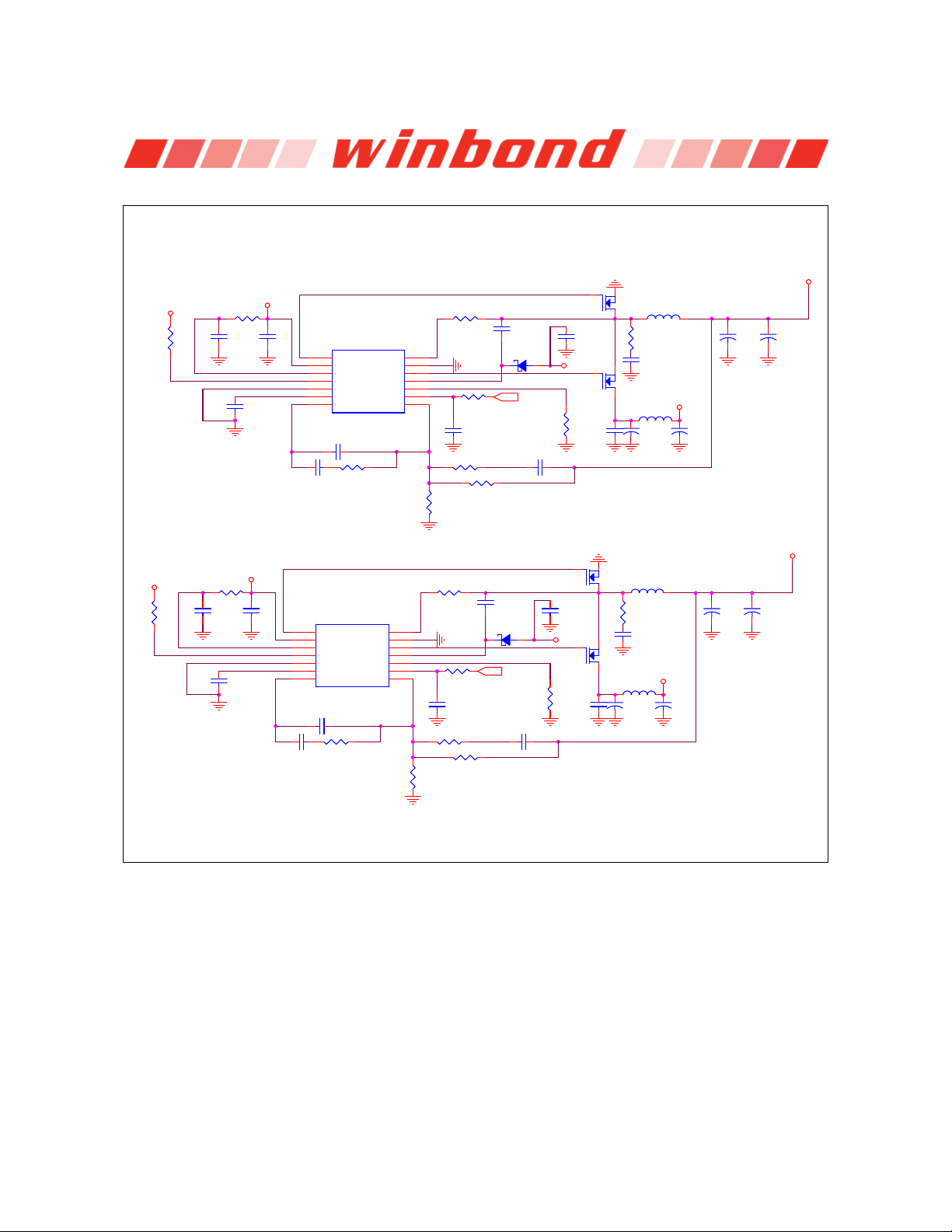
W83303AD/W83303AG
R33
4.7K
R23
4.7K
VPCI
VCC5
5VDUAL
VRAM
C55
2.2U
C40
2.2U
R31 10
R21 10
VCC5
C61
0.1U
C46
0.1U
C56
2.2U
5VDUAL
C41
2.2U
U2
1
LGATE
2
VDD
3
VDDA
4
PWOK
5
GNDA
6
SS
7 8
COMP FB
C51 (OPT)
C52
2.2n
U3
1
LGATE
2
VDD
3
VDDA
4
PWOK
5
GNDA
6
SS
7 8
COMP FB
W83320S
C66 (OPT)
100k
R37
C67
2.2n
100k
R27
BG_REF
W83320S
ISEN
GND
HGATE
BOOT
BG_REF
VREF
ISEN
GND
HGATE
BOOT
VREF
R30
5.1K(1%)
14
13
12
11
10
9
VRAM
NMOS
Q13
NMOS
Q11
NMOS
Q12
L4
Q10
L3
C64
2000U
L2
R34
2.2
C60
6.8n
1.5U
L1
R24
2.2
C45
6.8n
1.5U
C49
2000U
3.3U
VCC5
3.3U
5VDUAL
C65
1000U
C50
1000U
C58
2000U
C43
2000U
C59
2000U
C44
2000U
VPCI
R22
5.6K
C39
0.22U
D1
R29
5.1K(1%)
D2
SCHOTTKY
SCHOTTKY
VRAM_REF
C54
0.22U
VPCI_REF
49.9K
(OPT)
R36
C68
14
13
12
11
10
9
R25 33
C47
0.1U
R28
(OPT)
R32
5.6K
R35 33
C62
0.1U
R38
(OPT)
R39
R40
5.1k
(OPT)
49.9K
(OPT)
R26
C53
C57
2.2U
VCC5
C63
0.22u
C42
2.2U
5VDUAL
0.22U
C48
NMOS
- 14 -
Page 17
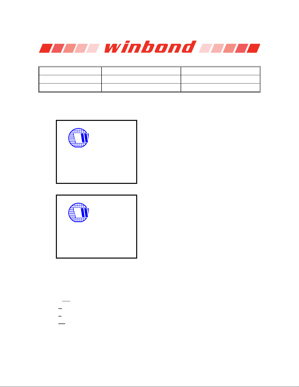
9. ORDERING INSTRUCTION
A
A
PART NO. PACKAGE REMARKS
W83303AD 48-pin LQFP
W83303AG 48-pin LQFP Pb-free package
10. HOW TO READ THE TOP MARKING
st
1
Line: Winbond Logo
nd
2
Line: Part No W83303AD, W83303AG (Pb-free package)
rd
3
Line: Wafer production serial number
th
4
Line: tracking code 410GBRA
410
:Date code, 410 means package was made in ’04 week 10
:Assembly ID, G means GR, A means ASE…etc.
G
:Chip Version, A means version A, B means version B
B
:Winbond internal use
RA
inbond
W83303AD
214658302
410GBR
inbond
W83303AG
214658302
410GBR
W83303AD/W83303AG
Publication Release Date: Jan. 9, 2006
- 15 - Revision 0.52
Page 18
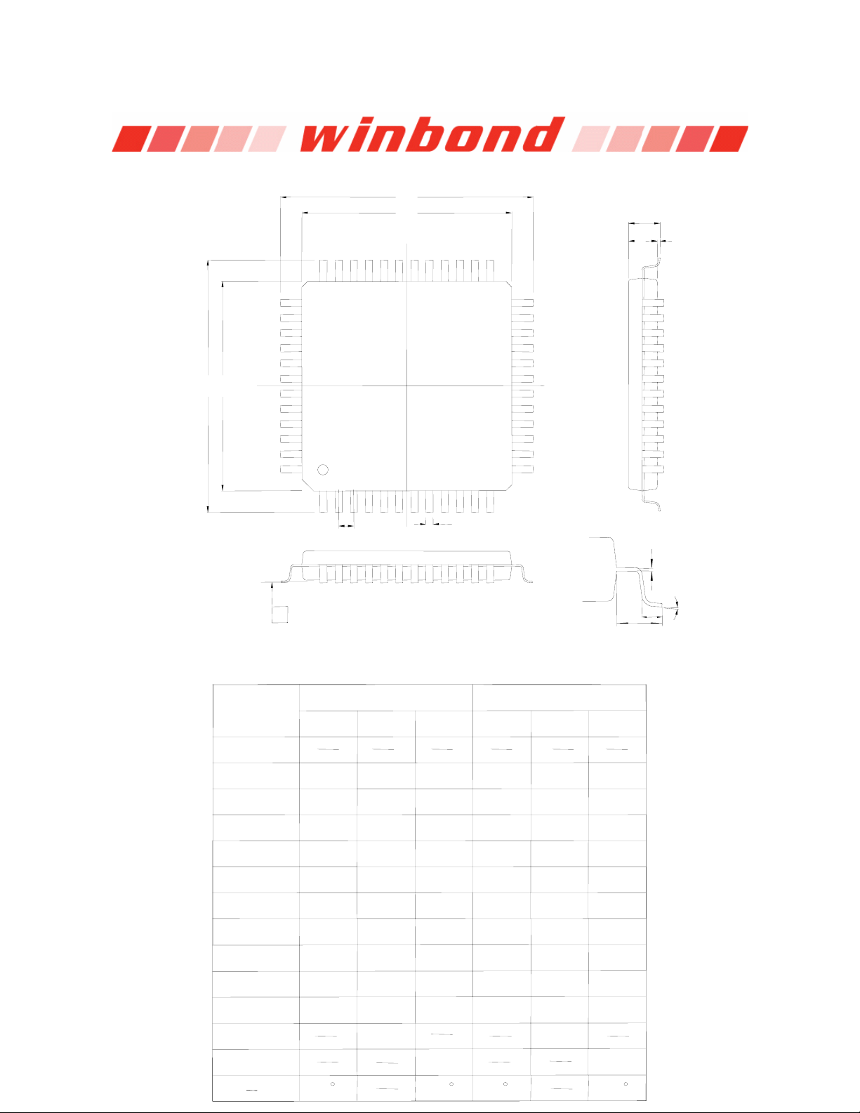
11. PACKAGE DIMENSION
H
H
A
Y
A A
36
W83303AD/W83303AG
D
A
A
25
E
SEATING PLANE
Controlling dimension: Millimeters
Symbol
37
48
24
1
Dimension in inch Dimension in mm
Min
Nom
Max Max
12
Mi
13
L1
No
1
2
b
D
E
e
H
D
H
E
L
1
0
0.002
0.053
0.006
0.004
0.272
0.272
0.014
0.350
0.018
0.004 0.006 0.15
0.0570.055
0.008
0.006 0.15
0.276
0.276
0.020
0.354
0.024
0.039
0.010
0.008
0.280
0.280
0.026
0.030
0.004
1.35
0.15
0.10
6.90
6.90
0.35
8.90
8.900.358
0.100.05
1.40
0.20
7.00
7.00
0.50
0.600.45
1.00
1.45
0.25
0.20
7.10
0.65
9.10 9.00
0.75
0.10
Page 19

W83303AD/W83303AG
Please note that all data and specifications are subject to change without notice. All the trademarks of
products and companies mentioned in this data sheet belong to their respective owners.
Important Notice
Winbond products are not designed, intended, authorized or warranted for use as components
in systems or equipment intended for surgical implantation, atomic energy control instruments,
airplane or spaceship instruments, transportation instruments, traffic signal instruments,
combustion control instruments, or for other applications intended to support or sustain life.
Further more, Winbond products are not intended for applications wherein failure of Winbond
products could result or lead to a situation wherein personal injury, death or severe property
or environmental damage could occur.
Winbond customers using or selling these products for use in such applications do so at their
own risk and agree to fully indemnify Winbond for any damages resulting from such improper
use or sales.
Publication Release Date: Jan. 9, 2006
- 17 - Revision 0.52
Page 20

 Loading...