

Page 1
3
PRELIMINARY
Spread Spectrum FTG for VIA K7 Chipset
Features
• Maximized EMI Suppression using Cypress’s Spread
Spectrum technology
• Single-chip system frequency synthesizer for VIA K7
chipset
• Two copies of CPU output
• Six copies of PCI output
• One 48-MHz output for USB
• One 24-MHz or 48-MHz output for SIO
• Two buffered reference outputs
• Thirteen SDRAM outputs provide support for 3 DIMMs
• Supports frequencies up to 200 MHz
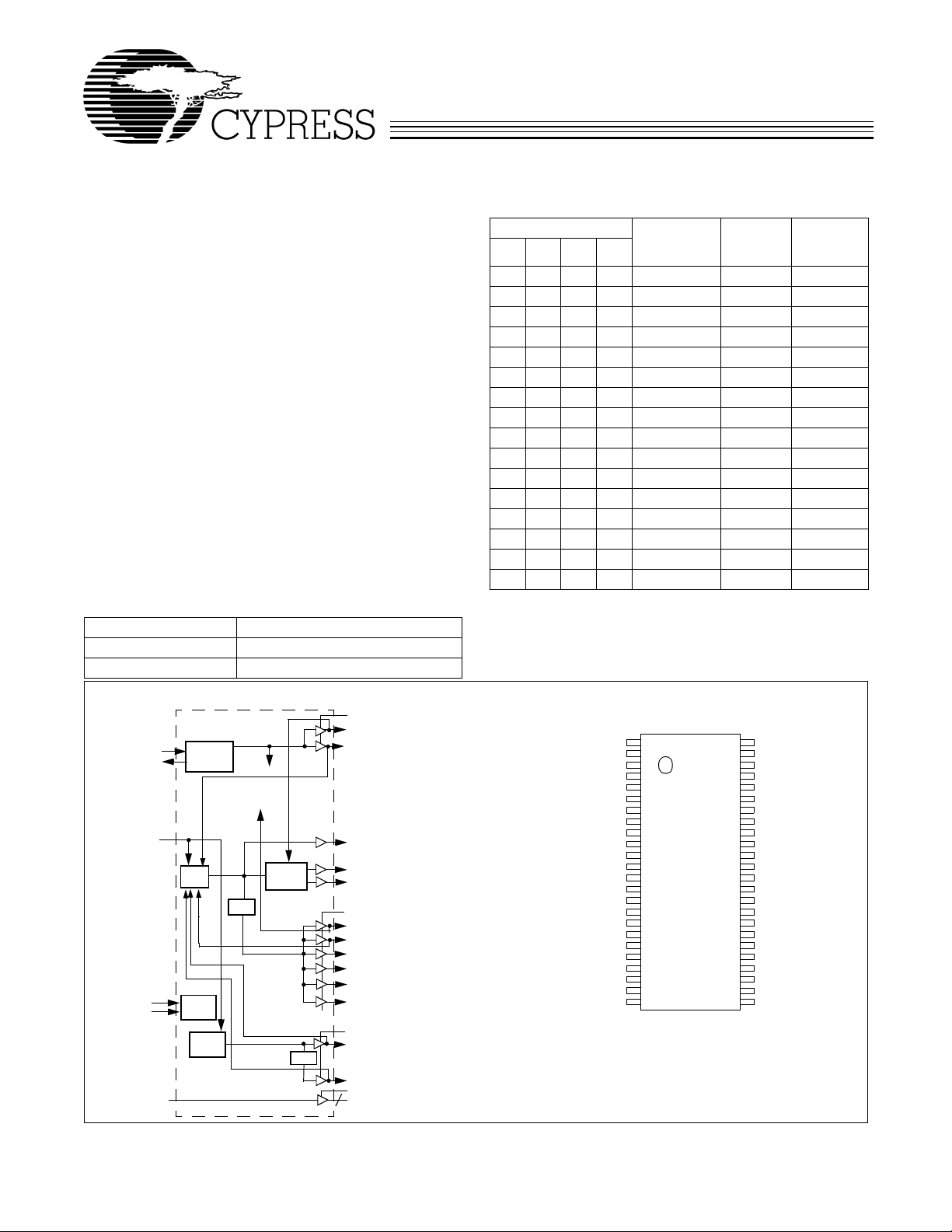
2
•I
C™ interface for programming
• Power management control inputs
• Available in 48-pin SSOP
Key Specifications
CPU to CPU Output Skew:.........................................175 ps
PCI to PCI Output Skew:............................................ 500 ps
: .................................................................... 3.3V±5%
V
DDQ3
SDRAMIN to SDRAM0:12 Delay:..........................3.7 ns typ.
Table 1. Mode Input Table
Mode Pin 2
0CPU_STOP#
1REF0
Block Diagram
VDDQ3
REF0/(CPU_STOP#)
X1
X2
PWRDWN#
SDATA
SCLK
SDRAMIN
I2C is a trademark of Phillips Corporation.
PLL 1
I2C
Logic
PLL2
XTAL
OSC
÷2,3,4
PLL Ref Freq
I/O Pin
Control
Control
Stop
Clock
÷2
REF1/FS0
CPU_CS
CPUT0
CPUC0
VDDQ3
PCI0/MODE
PCI1/FS1
PCI2
PCI3
PCI4
PCI5
VDDQ3
48MHz/FS2
24_48MHz/FS3
VDDQ3
SDRAM0:12
13
W230-03
Table 2. Pin Selectable Frequency
Input Address CPU_CS
1111 100.0 33.3 –0.5%
1110 100.0 33.3 OFF
1 1 0 1 100.0 33.3 ±0.5%
1100 95.0 31.7 OFF
1011 133.3 33.3 –0.5%
1010 133.3 33.3 OFF
1 0 0 1 133.3 33.3 ±0.5%
1000 102.0 34.0 OFF
0111 104.0 34.6 OFF
0110 106.0 35.3 OFF
0101 107.0 35.6 OFF
0100 108.0 36.0 OFF
0011 109.0 36.3 OFF
0 0 1 0 110.0 36.6 OFF
0 0 0 1 111.0 37.0 OFF
0 0 0 0 112.0 37.3 OFF
Pin Configuration
REF0/(CPU_STOP#)
Note:
1. Internal pull-up resistors should not be relied upon for setting I/O
VDDQ3
GND
VDDQ3
PCI0/MODE
PCI1/FS1*
GND
PCI2
PCI3
PCI4
PCI5
VDDQ3
SDRAMIN
GND
SDRAM11
SDRAM10
VDDQ3
SDRAM9
SDRAM8
GND
SDATA
I2C
{
SCLK
pins HIGH. Pin function with parentheses determined by MODE pin
resistor strapping. Unlike other I/O pins, input FS3 has an internal
pull-down resistor.
X1
X2
CPUT0
(MHz)
[1]
1
2
3
4
5
6
7
8
9
10
11
12
13
14
15
16
17
18
19
20
21
22
23
24
PCI 0:5
(MHz)
48
REF1/FS0*
47
GND
46
CPU_CS
45
GND
44
CPUC0
43
CPUT0
42
VDDQ3
41
PWRDWN#*
40
W230-03
SDRAM12
39
GND
38
SDRAM0
37
SDRAM1
36
VDDQ3
35
SDRAM2
34
SDRAM3
33
GND
32
SDRAM4
31
SDRAM5
30
VDDQ3
29
SDRAM6
28
SDRAM7
27
VDDQ3
26
48MHz/FS2*
25
24_48MHz/FS3^
Spread
SpectrumFS3 FS2 FS1 FS0
Cypress Semiconductor Corporation • 3901 North First Street • San Jose • CA 95134 • 408-943-2600
Document #: 38-07357 Rev. *A Revised December 26, 2002
Page 2
PRELIMINARY
W230-03
Pin Definitions
Pin Name Pin No. Pin Type Pin Description
CPUT0,
CPUC0,
CPU_CS 46 O CPU Clock Output for Chipset: CPU_CS is the push-pull clock output for the
PCI2:5 10, 11, 12, 13 O PCI Clock Outputs 2 through 5: These four PCI clo ck output s ar e contro lled by
PCI1/FS1 8 I/O Fixed PCI Clock Outpu t/Frequ ency Select 1: As an outp ut, frequ ency is set by
PCI0/MODE 7 I/O Fixed PCI Clock Output/Mode: As an outpu t, frequency is se t by the FS0:3 inpu ts
PWRDWN# 41 I PWRDWN# Input: LVTTL-comp atible inpu t that plac es the de vice in p ower-down
48MHz/FS2 2 6 I/O 48-MHz Output/Frequency Se lect 2: 4 8 MHz i s provided in norm al opera tion. In
24_48MHz/
FS3
REF1/FS0 48 I/O Reference Clock Output 1/Freque ncy Select 2: 3.3V 14.318-M Hz output clock.
REF0/
CPU_STOP
#
SDRAMIN 15 I Buffered Input Pin: Th e signal provide d to this input pin is buffered to 13 ou tputs
SDRAM0:12 38, 37, 35,
SCLK 24 I Clock pin for I
SDATA 23 I/O Data pin for I
X1 4 I Crystal Connection or External Reference Frequency I nput: This pin has d ual
X2 5 I Crystal Connection: An input connection for an external 14.318-MHz crystal. If
VDDQ3 1, 6, 14, 19,
GND 3, 9, 16, 22,
43, 44 O
(open-drain)
25 I/O 24_48-MHz Output/Frequency Select 3: In standard PC systems, this output can
2 I/O Reference Clock Output 0 or CPU_STOP# Input Pin: Function is determined
O Buffered Outputs: These thirteen dedicated outputs provide copies of the signal
34, 32, 31,
29, 28, 21,
20, 18, 17, 40
P Power Connection: Power supply for core logi c, PLL ci rcu itry, SDRAM outputs,
27, 30, 36, 42
G Ground Connections: Connect all ground pins to the common system ground
33, 39, 45, 47
CPU Clock Output 0: CPUT0 and CPUC0 are the dif ferential CPU clo ck outputs
for the K7 processor.
chipset. It has the same phase relationship as CPUT0.
the PWRDWN# control pin. Frequency is set by FS0:3 inputs or through serial
input interface, see Tables 2 and 6 for details. Output voltage swing is controlled
by voltage applied to VDDQ3.
FS0:3 inputs or through serial input interface. This output is controlled by the
PWRDWN# input. This pin also serves as a power-on strap option to determine
device operating frequency as described in Table 2.
or through serial input interface, see Tables 2 and 6. This output is controlled by
the PWRDWN# input. This pin also serves as a power-on strap option to determine
the function of pin 2, see Table 1 for details.
mode when held LOW. In power-down mode, CPUC0 will be three-sta ted and al l
the other output clocks will be driven LOW.
standard PC systems, this output can be used as the reference fo r the Uni ver sal
Serial Bus host controller. This pin also serves as a power on strap option to
determine device operating frequency as described in Table 2.
be used as the cloc k input for a Sup er I/O chip. T he output frequ ency is control led
by Configuration Byte 3 bit[6]. The default output frequency is 48 MHz. This pin
also serves as a power-on strap option to determine device operating frequency
as describe d in Table 2.
This pin also serves as a power-on strap option to determine device operating
frequency as describ ed in T able 2. Upon power-u p, FS0 input will be latched whic h
will set clock frequencies as described in Table 2.
by the MODE pin. When CPU_STOP# input is asserted LOW, it will drive CPUT0
and CPU_CS to logic 0, an d it will three-sta te CPUC0. When thi s pin is configured
as an output , this pin becomes a 3.3V 14 .318-MHz output clock.
(SDRAM0:12).
provided at the SDRAMIN in put . The sw in g is set by VDDQ 3, and they are deactivated when PWRDWN# input is set LOW.
2
C circuitry.
2
C circuitry.
functions. It can be used as an external 14.318-MHz crystal connection or as an
external reference frequency input.
using an external reference, thi s pin must be left unconnected.
PCI outputs, reference ou tputs, 48-M Hz output, a nd 24_48-MH z output. Connect
to 3.3V supply
plane.
Document #: 38-07357 Rev. *A Page 2 of 15
Page 3
PRELIMINARY
Overview
The W230-03 was developed as a single-chip device to meet
the clocking needs of VIA K7 core logic chip sets. In addition
to the typical output s provided by a standa rd FTG, the W23003 adds a thirteenth output buffer, supporting SDRAM DIMM
modules in conjunction with the chipset.
Cypress’s proprietary spread spectrum frequency synthesis
technique is a feature of the CPU and PCI outputs. When enabled, this feature reduces the peak EM I measurements of n ot
only the output signals and their harmonics, but also of any
other clock signals that are properly synchronized to them.
Functional Description
I/O Pin Operation
Pins 7, 8, 25, 26, and 48 are dual-purpose l/O pins. Upon
power-up these pins act as logic inputs, allowing the determination of assigned device functions. A short time after powerup, the logic state of each pin is latched and the pins become
clock outputs. This feature reduces device pin count by combining clock outputs with inp ut sel ec t pins .
An external 10 -kΩ “strapping” resistor is connected between
the l/O pin and ground or V
latch to “0,” connect ion to V
Figure 2 show two suggested methods for strapping resistor
connections.
. Connection to ground sets a
DD
sets a latch to “1.” Figure 1 and
DD
W230-03
Upon W230-03 power-up, the first 2 ms of operation is used
for input logic selection. During this period, the five I/O pin s (7,
8, 25, 26, 48) are three-stated, allowing the output strapping
resistor on the l/O pins to pull the pins and their associated
capacitive clock load to either a logic HIGH or LOW state. At
the end of the 2- ms period, the establ ished logic “0” or “1”
condition of the l/O pin is latched. Next the output buffer is
enabled converting the l/O pins into operating clock outputs.
The 2-ms timer starts when V
can only be reset by turning V
It should be noted that the strapping resistors have no significant effect on clock output signal integrity. The drive impedance of clock outputs is <40Ω (nominal), which is minimally
affected by th e 1 0-k Ω str a p t o gro u nd or V
ries termination resistor, the output strapping resistor should
be placed as close to the l/O pin as possible in order to keep
the interc onne cti ng t race sh ort . Th e trac e fr om the res isto r to
ground or V
to prevent system noise coupling during input logic sampling.
should be kept less than two inches in length
DD
When the clock outputs are enabled following the 2-ms input
period, the specified output frequency is delivered on the pin,
assuming that V
full value, outpu t frequency initial ly may be below ta rget but will
has stabilized . If VDD has not yet reached
DD
increase to target once V
case, a short output clock cycle may be produced from the
CPU clock outputs when the outputs are enabled.
V
DD
reaches 2.0V. The input bits
DD
off and then back on again.
DD
. As with the se-
DD
voltage has stabilized. In either
DD
Output Strapping Resistor
W230-03
Power-on
Reset
Timer
W230-03
Power-on
Reset
Timer
10 k
Output Three-state
Output
Buffer
Hold
Output
Low
QD
Data
Latch
(Load Option 1)
(Load Option 0)
10 k
Ω
Ω
Figure 1. Input Logic Selection Through Resistor Load Option
Jumper Options
V
DD
Ω
10 k
Output
Buffer
Output Three-state
Hold
Output
Low
QD
Data
Latch
Resistor Value R
Series Termination Resistor
R
Output Strapping Resistor
Series Termination Resistor
R
Clock Load
Clock Load
Figure 2. Input Logic Selection Through Jumper Option
Document #: 38-07357 Rev. *A Page 3 of 15
Page 4
PRELIMINARY
Spread Spectrum Frequency Timing Generator
The device generates a clock that is frequency modulated in
order to increase th e bandwidt h that it occu pies. By inc reasing
the bandwidth of the fundamental and its harmonics, the amplitudes of the radiated electromagnetic emissions are reduced. This effect is depicted in Figure 3.
As shown in Figure 3, a harmonic of a modulated clock has a
much lower amplit ude than that of an unmodulated si gnal. The
reduction in amplitude is dependent on the harmonic number
and the frequency deviation or spread. The equation for the
reduction is:
dB = 6.5 + 9*log
Amplitude (dB)
(P) + 9*log10(F)
10
SSFTG Typical Clock
W230-03
Where P is the pe rcentage of deviation and F is the frequenc y
in MHz where the reduction is measured.
The output clock is modulated with a waveform depicted in
Figure 4. This waveform, as discusse d in “Spread Spectrum
Clock Generation for the Reduction of Radiated Emi ssions” by
Bush, Fessler, and Hardin produces the maximum reduction
in the amplitude of radiated electromagnetic emissions. The
deviation select ed for this ch ip is spec ified in Table 6. Fi gure 4
details the Cypress spread ing patt ern. Cypre ss does of fer o ptions with more spread and greater EMI reduction. Contact
your local Sales representative for details on these devices.
Spread Spectrum clocking is activated or deactivated by selecting the approp riate v alues for bits 1 –0 in da ta byt e 0 of th e
2
C data stream. Refer to Table 6 for more details.
I
EMI Reduction
Spread
Spectrum
Enabled
Amplitude (dB)
Non-
Spread
Speactrum
Frequency Span (MHz)
Center Spread
Frequency Span (MHz)
Down Spread
Figure 3. Clock Harmonic with and without SSCG Modulation Frequency Domain Representation
MAX (0%)
10%
20%
30%
40%
50%
60%
70%
80%
FREQUENCY
MIN (–0.5%)
90%
100%
10%
20%
30%
40%
50%
60%
70%
80%
90%
Figure 4. Ty pical Modulation Profile
100%
Document #: 38-07357 Rev. *A Page 4 of 15
Page 5
PRELIMINARY
Serial Data In te rface
The W230-03 features a two-pin, serial data interface that can
be used to configure inte rnal regi ster settin gs that con trol particular device functions. Upon power-up, the W230-03 initializes with default reg ist er s ett ing s, ther efore the use of this serial data interface is optional. The serial interface is write-only
(to the clock chip) and is the dedica ted func tion of dev ice pin s
SDATA and SCLOCK. In motherboard applications, SDATA
and SCLOCK are typically driven by two logic outputs of the
Table 3. Serial Data Interface Control Functions Summary
Control Function Description Common Application
Clock Output Disable Any individual cloc k output(s) ca n be disabled . Dis-
abled outputs are actively held LOW.
CPU Clock Frequency
Selection
Spread Spectrum
Enabling
Output Three-state Puts clock output into a high impedance state. Production PCB testing.
(Reserved) Reserved function for future devic e revisi on or pro-
Provides CPU/PCI frequency selections through
software. Frequency is changed in a smooth and
controlled fashion.
Enables or disables spread spectrum clocking. For EMI reduction.
duction device testing .
chipset. Clock device register changes are normally made
upon system initialization, if any are required. The interface
can also be used during system opera tio n for power manag ement functions. Ta b l e 3 summa rizes the contro l functions of
the serial data interface.
Operation
Data is written to the W230-03 in eleven bytes of eight bits
each. Bytes are written in the order shown in Table 4.
Unused outputs are disabled to reduce EMI
and system power. Examples are clock outputs to unused PCI slots.
For alternate microprocessors and power
management options. Sm ooth frequency transition allows CPU frequency change under
normal system operation.
No user application. Regi ster bit mus t be written as 0.
W230-03
Table 4. Byte Writing Sequence
Byte Sequence Byte Name Bit Sequence Byte Description
1 Sla ve Address 1 1010010 Commands the W230-03 to ac cept the bits in D ata Bytes 0–6 for internal
2 Command
Code
3 Byte Count Don’t Care Unused by the W230-0 3, therefore bit values are i gnored (“don’t care”).
4 Data Byte 0 Refer to Table 5 The data bits in Data Bytes 0–7 set internal W230-03 registers that
5Data Byte 1
6Data Byte 2
7Data Byte 3
8Data Byte 4
9Data Byte 5
10 Data Byte 6
11 Data Byte 7
Don’t Care Unused by the W230-0 3, therefore bi t values are i gnored (“don’t care”).
register configurati on. Since o ther dev ices may e xist o n the sa me co mmon serial data bus, it is necessary to have a specific slave address for
each potential rec eiver. The slave receiver addres s f or the W230-03 is
1 10100 10. Re giste r settin g wi ll not be mad e if th e Slave Addres s is n ot
correct (or is for an alternate slave receiver).
This byte must be include d in the data write sequence to mainta in proper
byte allocation. The Com mand Co de Byte is par t of the standar d serial
communication protocol and may be used when writing to another addressed slave receiver on the serial data bus.
This byte must be include d in the data write sequence to mainta in proper
byte allocation. Th e Byte C o unt Byte is part of the standard serial communication protocol and may be used when writing to another addressed slave receiver on the serial data bus.
control device op erat ion . The data bits are only accepted when the Address Byte bit sequence is 11010010, as noted above. For description
of bit control functions, re fer to Table 5, Data Byte Serial Configuration
Map.
Document #: 38-07357 Rev. *A Page 5 of 15
Page 6

PRELIMINARY
Writing Data Bytes
Each bit in the da ta byt es co ntro ls a p articular device function
except for the “reserved” bits, which must be written as a logi c
0. Bits are written MSB (most significant bit) first, which is bit
Table 5. Da ta Bytes 0–7 Serial Configuration Map
Affected Pin
Bit(s)
Data Byte 0
7 -- -- (Reserved) -- -- 0
6 -- -- SEL_2 See Table 6 0
5 -- -- SEL_1 See Table 6 0
4 -- -- SEL_0 See Table 6 0
3 -- -- Hardware/Software Frequency
2 -- -- SEL_4 See Table 6 1
1 -- -- SEL_3 See Table 6 0
0 -- -- Normal Three-stated 0
Data Byte 1
7 -- -- (Reserved) -- -- 0
6 -- -- (Reserved) -- -- 0
5 -- -- (Reserved) -- -- 0
4 -- -- (Reserved) -- -- 0
3 -- -- (Reserved) Write to ‘1’ -- -- 1
2 -- -- (Reserved) Write to ‘1’ -- -- 1
1 -- -- (Reserved) Write to ‘1’ -- -- 1
0 -- -- (Reserved) Write to ‘1’ -- -- 1
Data Byte 2
7 -- -- (Reserved) -- -- 0
6 7 PCI0 Clock Output Disable Low Active 1
5 -- -- (Reserved) -- -- 0
4 13 PCI5 Clock Output Disable Low Active 1
3 12 PCI4 Clock Output Disable Low Active 1
2 11 PCI3 Clock Output Disable Low Active 1
1 10 PCI2 Clock Output Disable Low Active 1
0 8 PCI1 Clock Output Disable Low Active 1
Data Byte 3
7 -- -- (Reserved) -- -- 0
6 -- SEL_48MHz SEL 48MHz as the output fre-
5 26 48MHz Clock Outp ut Di sable Low Active 1
4 25 24_48MHz Clock Output Disable Low Active 1
3 -- -- (Reserved) -- -- 0
2 21, 20,
18, 17
SDRAM8:11 Clock Output Disable Low Active 1
Control Function
Select
quency for 24_48MHz
7. Table 5 gives the bit formats for registers located in Data
Bytes 0–7.
Ta ble 6 details additional frequency selections that are available through the serial data interface.
Bit Control
Hardware Software 0
24-MHz 48-MHz 0
W230-03
DefaultPin No. Pin Name 0 1
Document #: 38-07357 Rev. *A Page 6 of 15
Page 7

PRELIMINARY
Table 5. Da ta Bytes 0–7 Serial Configuration Map (continued)
Affected Pin
Bit(s)
1 32, 31,
29, 28
0 38, 37,
35, 34
Data Byte 4
7 -- -- (Reserved) -- -- 0
6 -- -- (Reserved) -- -- 0
5 -- -- (Reserved) -- -- 0
4 -- -- (Reserved) -- -- 0
3 -- -- (Reserved) -- -- 0
2 -- -- (Reserved) -- -- 0
1 -- -- (Reserved) -- -- 0
0 -- -- (Reserved) -- -- 0
Data Byte 5
7 -- -- (Reserved) -- -- 0
6 -- -- (Reserved) -- -- 0
5 -- -- (Reserved) -- -- 0
4 -- -- (Reserved) -- -- 1
3 -- -- (Reserved) -- -- 0
2 -- -- (Reserved) -- -- 0
1 48 REF1 Clock Output Disable Low Active 1
0 2 REF0 Clock Output Disable Low Active 1
Data Byte 6
7 -- -- (Reserved) -- -- 0
6 -- -- (Reserved) -- -- 0
5 -- -- (Reserved) -- -- 0
4 -- -- (Reserved) -- -- 0
3 -- -- (Reserved) -- -- 0
2 -- -- (Reserved) -- -- 0
1 -- -- (Reserved) -- -- 0
0 -- -- (Reserved) -- -- 0
Data Byte 7
7 -- -- (Reserved) -- -- 0
6 -- -- (Reserved) -- -- 0
5 -- -- (Reserved) -- -- 0
4 -- -- (Reserved) -- -- 0
3 -- -- (Reserved) -- -- 0
2 -- -- (Reserved) -- -- 0
1 -- -- (Reserved) -- -- 0
0 -- -- (Reserved) -- -- 0
SDRAM4:7 Clock Output Disable Low Active 1
SDRAM0:3 Clock Output Disable Low Active 1
Control Function
Bit Control
W230-03
DefaultPin No. Pin Name 0 1
Document #: 38-07357 Rev. *A Page 7 of 15
Page 8

PRELIMINARY
Table 6. Additional Frequency Selections through Serial Data Interface Data Bytes
Input Conditions Output Frequency
Data Byte 0, Bit 3 = 1
Bit 2
SEL_4
11111 100.0 33.3 –0.5%
11110 100.0 33.3 OFF
11101 100.0 33.3 ±0.5%
11100 95.0 31.7 OFF
11011 133.3 33.3 –0.5%
11010 133.3 33.3 OFF
11001 133.3 33.3 ±0.5%
11000 102.0 34.0 OFF
10111 104.0 34.6 OFF
10110 106.0 35.3 OFF
10101 107.0 35.6 OFF
10100 108.0 36.0 OFF
10011 109.0 36.3 OFF
10010 110.0 36.6 OFF
10001 111.0 37.0 OFF
10000 112.0 37.3 OFF
01111 113.0 37.6 OFF
01110 114.0 38.0 OFF
01101 115.0 38.3 OFF
01100 116.0 38.6 OFF
01011 118.0 39.3 OFF
01010 120.0 40.0 OFF
01001 124.0 31.0 OFF
01000 127.0 31.7 OFF
00111 130.0 32.5 OFF
00110 136.0 34.0 OFF
00101 140.0 35.0 OFF
00100 145.0 36.2 OFF
00011 150.0 37.5 OFF
00010 155.0 38.7 OFF
00001 160.0 40 OFF
00000 166.0 41.6 OFF
Bit 1
SEL_3
Bit 6
SEL_2
Bit 5
SEL_1
Bit 4
SEL_0
CPU PCI Spread Spectrum
W230-03
Document #: 38-07357 Rev. *A Page 8 of 15
Page 9

PRELIMINARY
Absolute Maximum Ratings
Stresses greater than those listed i n this tabl e may cau se permanent damage to the devic e. These represent a stre ss rating
only. Operation of the device at these or any other conditions
.
[2]
above those sp eci fie d in the operating sections of this s pe cification is not implied. Maximum conditions for extended periods may affect reli abi li ty.
W230-03
Parameter Description Rating Unit
, V
V
DD
IN
T
STG
T
B
T
A
T
C
ESD
PROT
DC Electrical Characteristics: T
Voltage on any pin with respect to GND –0.5 to +7.0 V
Storage Temperature –65 to +150 °C
Ambient Temperature under Bias –55 to +125 °C
Operating Temperature 0 to +70 °C
Case Temperature 115 °C
Input ESD Protection 2 (min.) kV
= 0°C to +70°C, V
A
= 3.3V±5%
DDQ3
Parameter Description Test Condition Min. Typ. Max. Unit
Supply Current
I
I
DD
DD
3.3V Supply Current CPUT0, CPUC0,
CPU_CS =100 MHz
Outputs Loaded
2.5V Supply Current CPUT0, CPUC0,
CPU_CS =100 MHz
Outputs Loaded
[3]
[3]
260 mA
25 mA
Logic Inputs
V
IL
V
IH
I
IL
I
IH
Input Low Voltage GND – 0.3 0.8 V
Input High Voltage 2.0 VDD + 0.3 V
Input Low Current
Input High Current
[4]
[4]
–25 µA
10 µA
Clock Outputs
V
V
V
V
I
OL
OH
OL
OH
OL
Output Low Voltage I
Output High Voltage IOH = –1 mA 3.1 V
Output Low Voltage CPU_CS,
CPUT0, CPUC0
Output High Voltage CPU_CS,
CPUT0, CPUC0
Output Low Current PCI0:5 VOL = 1.5V 70 110 135 mA
REF0:1 V
48 MHz V
24 MHz V
SDRAM0:12 V
I
OH
Output High Current PCI0:5 V
REF0:1 V
48 MHz V
24 MHz V
SDRAM0:12 V
Notes:
Multiple Supplies: The Voltage on any input or I/O pin cannot exceed the power pin during power-up. Power supply sequencing is NOT required.
2.
3. All clock outputs loaded with 6" 60Ω transmission lines with 20-pF capacitors.
4. W230-03 logic inputs (except FS3) have internal pull-up devices (pull-ups not full CMOS level). Logic input FS3 has an internal pull-down device.
= 1 mA 50 mV
OL
Termination to V pull-up
00.3V
(external)
Termination to V pull-up
1.0 1.2 V
(external)
= 1.5V 50 70 100 mA
OL
= 1.5V 50 70 100 mA
OL
= 1.5V 50 70 100 mA
OL
= 1.5V 70 110 135 mA
OL
= 1.5V 70 110 135 mA
OH
= 1.5V 50 70 100 mA
OH
= 1.5V 50 70 100 mA
OH
= 1.5V 50 70 100 mA
OH
= 1.5V 70 110 135 mA
OH
Document #: 38-07357 Rev. *A Page 9 of 15
Page 10

DC Electrical Characteristics: T
PRELIMINARY
= 0°C to +70°C, V
A
DDQ3
= 3.3V±5% (continued)
W230-03
Parameter Description Test Condition Min. Typ. Max. Unit
Crystal Oscillator
[7]
[5]
V
= 3.3V 1.65 V
DDQ3
14 pF
Pin X2 unconnected 28 pF
V
TH
C
LOAD
C
IN,X1
X1 Input Threshold Voltage
Load Capacitance, Imposed on
External Crystal
[6]
X1 Input Capacitance
Pin Capacitance/Inductance
C
C
L
IN
OUT
IN
Input Pin Capacitance Except X1 and X2 5 pF
Output Pin Capacitance 6 pF
Input Pin Inductance 7nH
AC Electrical Characteristics
= 0°C to +70°C, V
T
A
AC clock parameters are tested and guaranteed over stated operating conditions using the stated lump capacitive load at the
clock output; Spread Spectrum is disabled.
CPU Clock Outputs (CPUT0, CPUC0, CPU_CS)
Parameter Description Test Condition/Comments
t
R
t
F
t
D
t
JC
f
ST
Output Rise Edge Rate 1.0 1.0 V/ns
Output Fall Edge Rate 1.0 1.0 V/ns
Duty Cycle Measured at 50% point 50 50 %
Jitter, Cycle to Cycle 250 250 ps
Frequency Stabilization
from Power-up (cold
start)
Z
o
Notes:
5. X1 input threshold voltage (typical) is V
6. The W230-03 contains an internal crystal load capacitor between pin X1 and ground and another between pin X2 and ground. Total load placed on crystal is
14 pF; this includes typical stray capacitance of short PCB traces to crystal.
7. X1 input capacitance i s applicable when driv ing X1 with an external clock source (X2 is left unconnected).
8. Refer to Figure 5 for K7 operation clock driver test circuit.
AC Output Impedance VO = V
= 3.3V±5%, f
DDQ3
= 14.31818 MHz
XTL
[8]
Assumes full supply v oltage reached
within 1 ms from power-up. Short
cycles exist prior to frequency
stabilization.
X
/2.
DD
CPU = 100 MHz CPU = 133 MHz
UnitMin. Typ. Max. Min. Typ. Max.
33ms
50 50 Ω
Document #: 38-07357 Rev. *A Page 10 of 15
Page 11

PRELIMINARY
W230-03
PCI Clock Outputs, PCI0:5 (Lump Capacitance Test Load = 30 pF
Parameter Description Test Condition/Comments Min. Typ. Max. Unit
t
t
t
t
t
t
t
t
t
f
Z
P
H
L
R
F
D
JC
SK
O
ST
o
Period Measured on rising edge at 1.5V 30 ns
High Time Duration of clock cycle above 2.4V 12 ns
Low Time Duration of clock cycle below 0.4V 12 ns
Output Rise Edge Rate Measured from 0.4V to 2.4V 1 4 V/ns
Output Fall Edge Rate Measured from 2.4V to 0.4V 1 4 V/ns
Duty Cycle Measured on rising and falling edge at 1.5V 45 55 %
Jitter, Cycle-to-Cycle Measured on rising edge at 1.5V. Maximum
250 ps
difference of cycle time between two adja cent cycles.
Output Skew Measured on rising edge at 1.5V 500 ps
CPU to PCI Clock Skew Covers all CPU/PCI outputs. Measured on rising
1.5 4 ns
edge at 1.5V. CPU leads PCI output.
Frequency Stabilization
from Power-up (cold
start)
AC Output Impedance Average value during switching transition. Used for
Assumes full supply voltage reached within 1 ms
from power-up. Short cycles exist prior to frequen cy
stabilization.
3ms
30 Ω
determining series termination value.
REF0:1 Clock Outputs (Lump Capacitance Test Load = 20 pF)
Parameter Description Test Condition/Comments Min. Typ. Max. Unit
f Frequency, Actual Frequency generated by crystal oscillator 14.318 MHz
t
R
t
F
t
D
f
ST
Output Rise Edge Rate Measured from 0.4V to 2.4V 0.5 2 V/ns
Output Fall Edge Rate Measured from 2.4V to 0.4V 0.5 2 V/ns
Duty Cycle Measured on rising and falling edge at 1.5V 45 55 %
Frequency Stabilization from
Power-up (cold start)
Assumes full supply voltage reached within
1 ms from power-up. Short cycles exist pri or to
3ms
frequency stabilization.
Z
o
AC Output Impedance Average value during switching trans ition. Used
for determining series termination value.
40 Ω
48-MHz Clock Output (Lump Capacitance Test Load = 20 pF)
Parameter Description Test Condition/Comments Min. Typ. Max. Unit
f Frequency, Actual Determined by PLL divider ratio (see m/n below) 48.008 MHz
f
D
Deviation from 48 MHz (48.008 – 48)/48 +167 ppm
m/n PLL Ratio (14.31818 MHz x 57/17 = 48.008 MHz) 57/17
t
R
t
F
t
D
f
ST
Output Rise Edge Rate Measured from 0.4V to 2.4V 0.5 2 V/ns
Output Fall Edge Rate Measured from 2.4V to 0.4V 0.5 2 V/ns
Duty Cycle Measured on rising and falling edge at 1.5V 45 55 %
Frequency Stabilization
from Power-up (cold start)
Assumes full suppl y voltage re ached within 1 ms
from power-up. Short cycles exist prior to fre-
3ms
quency stabilizati on.
Z
o
AC Output Impedance Average value during switching transition. Used
for determining series terminati on va lue.
40 Ω
Document #: 38-07357 Rev. *A P age 11 of 15
Page 12

PRELIMINARY
W230-03
24-MHz Clock Output (Lump Capacitance Test Load = 20 pF)
Parameter Description Test Condition/Comments Min. Typ. Max. Unit
f Frequency, Actual Determined by PLL divider ratio (see m/n below) 24.004 MHz
f
D
Deviation from 24 MHz (24.004 – 24)/24 +167 ppm
m/n PLL Ratio (14.31818 MHz x 57/34 = 24.004 MHz) 57/34
t
R
t
F
t
D
f
ST
Output Rise Edge Rate Measured from 0.4V to 2.4V 0.5 2 V/ns
Output Fall Edge Rate Measured from 2.4V to 0.4V 0.5 2 V/ns
Duty Cycle Measured on rising and falling edge at 1.5V 45 55 %
Frequency Stabilization
from Power-up (cold start)
Assumes full suppl y voltage re ached within 1 ms
from power-up. Short cycles exist prior to fre-
3ms
quency stabilizati on.
Z
o
AC Output Impedance Average value during switching transition. Used
for determining series terminati on va lue.
CPUCLK_T
VDD
+
V1
3.3
-
Z0 = 52Ω
Length = 5”
R8
47
T1
Z0 = 52Ω
Length = 3
T2
1.5V
”
40 Ω
R1
68
20p
Clock Chip
Driver
CPU
Z0 = 52Ω
Length = 5”
T4
CPUCLK_C
R9
47
Figure 5. K7 Open Drain Clock Driver Tes t Circuit
Ordering Information
Ordering Code
W230-03 H 48-pin SSOP (300 mils)
Package
Name Package Type
Z0 = 52Ω
Length = 3
T5
1.5V
”
R3
68
20p
Document #: 38-07357 Rev. *A Page 12 of 15
Page 13

Layout Diagram
G
+3.3V Supply
FB
0.005 µF
C4
G
G
G
PRELIMINARY
V
C3
DDQ3
V
V
DDQ3
Core
G
G
10 µF
G G
1
2
3
4
G
5
V
6
G
7
8
G
9
G
10
11
12
G
13
V
14
G
15
16
48
G
47
46
G
45
44
G
43
V
42
G
41
W230-03
40
G
39
38
37
V
36
G
35
34
G
33
W230-03
G
G
17
G
18
G
19
20
V
G
21
G
22
23
G
24
FB = Dale ILB1206 - 300 (300Ω @ 100 MHz)
Ceramic C4 = 0.005
µ
C3 = 10–22
= VIA to GND plane layer
G
Note: Each supply plane or strip should have a
Document #: 38-07357 Rev. *A Page 13 of 15
F
V =VIA to respective supply plane layer
G
G
G
G
32
31
V
30
29
28
V
27
26
25
µF
C6 = 0.01
ferrite bead and capacitors
µ
F
G
G
Page 14

ng so indemnifies Cypress Semiconductor against all charges.
Package Diagram
PRELIMINARY
48-Pin Small Shrink Outline Package (SSOP, 300 mils)
W230-03
Summary of nominal dimensions in inches:
Body Width: 0.296
Lead Pitch: 0.025
Body Length: 0.625
Body Height: 0.102
Document #: 38-07357 Rev. *A Page 14 of 15
© Cypress Semiconductor Corporation, 2002. The information contained herein is subject to change without notice. Cypress Semiconductor Corporation assumes no responsibility for the use
of any circuitry other than circuitry embodied in a Cypress Semiconductor product. No r does it convey or imply any license under patent or other rights. Cypress Semiconductor does not autho rize
its products for use as critical components in life-support systems where a malfunction or failure may reasonably be expected to result in significant injury to the user. The inclusion of Cypress
Semiconductor products in life-support systems application implies that the manufacturer assume s all risk of such use and in doi
Page 15

PRELIMINARY
Document Title: W230-03 Spread Sp ectrum FTG for VIA K7 Chipset
Document Number: 38-07357
REV. ECN NO.
** 112252 02/13/02 DSG Change from Spec number: 38-01035 to 38-07357
*A 122905 12/26/02 RBI Add power up requirements to maximum ratings requirements.
Issue
Date
Orig. of
Change Description of Change
W230-03
Document #: 38-07357 Rev. *A Page 15 of 15
 Loading...