

Page 1
W170-01
Spread A ware ™, F reque ncy Multi plier and Zero Del ay Buffe r
Features
• Spread Aware ™—desi gned to work with SSFTG
reference signals
• T wo outputs
• Configuration options allow various multiplication of
the reference frequency, refer to
Table 1
to deter mine
the specific option which meets your multi p lication
needs
• Available in 8-pin SOIC package
Key Specific ati o n s
Operatin g Voltage: ........ .. .......... ....... 3 .3V±5% o r 5. 0 V ± 10 %
Operating Range: ... ........... .. .......20 MHz < f
OUT1
< 133 MHz
Absolute Jitter: .........................................................±500 ps
Output to Output Skew: ................. ............................. 250 ps
Propagation Delay: ......................................... .. .. ......±350 ps
Propagation delay is affected by input rise time.
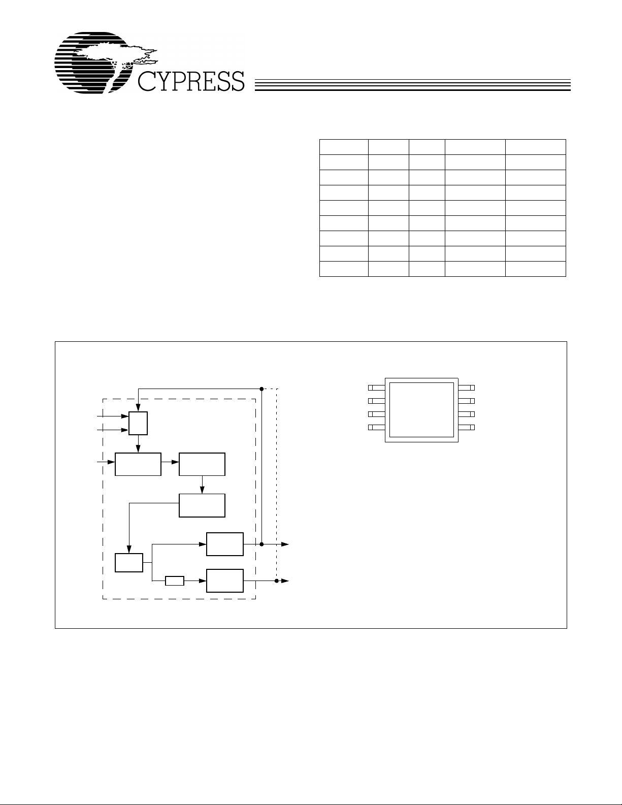
Block Diagram
External feedback connection to
OUT1 or OUT2, not both
FS0
FS1
FBIN
÷Q
T able 1. Configuration Options
FBIN FS0 FS1 OUT1 OUT2
OUT1 0 0 2 X REF REF
OUT1 1 0 4 X REF 2 X REF
OUT1 0 1 REF REF/2
OUT1 1 1 8 X REF 4 X REF
OUT2 0 0 4 X REF 2 X REF
OUT2 1 0 8 X REF 4 X REF
OUT2 0 1 2 X REF REF
OUT2 1 1 16 X REF 8 X REF
Pin Configuration
FBIN
IN
GND
FS0
1
2
3
4
8
7
6
5
OUT2
VDD
OUT1
FS1
IN
Reference
Input
Spread Aware is a trademark of Cypress Semiconductor Corporation.
Phase
Detector
VCO
÷2
Charge
Pump
Loop
Filter
Output
Buffer
Output
Buffer
OUT1
OUT2
Cypress Semiconductor Corporation
• 3901 North First Street • San Jose • CA 95134 • 408-943-2600
September 28, 1999, r ev . **
Page 2
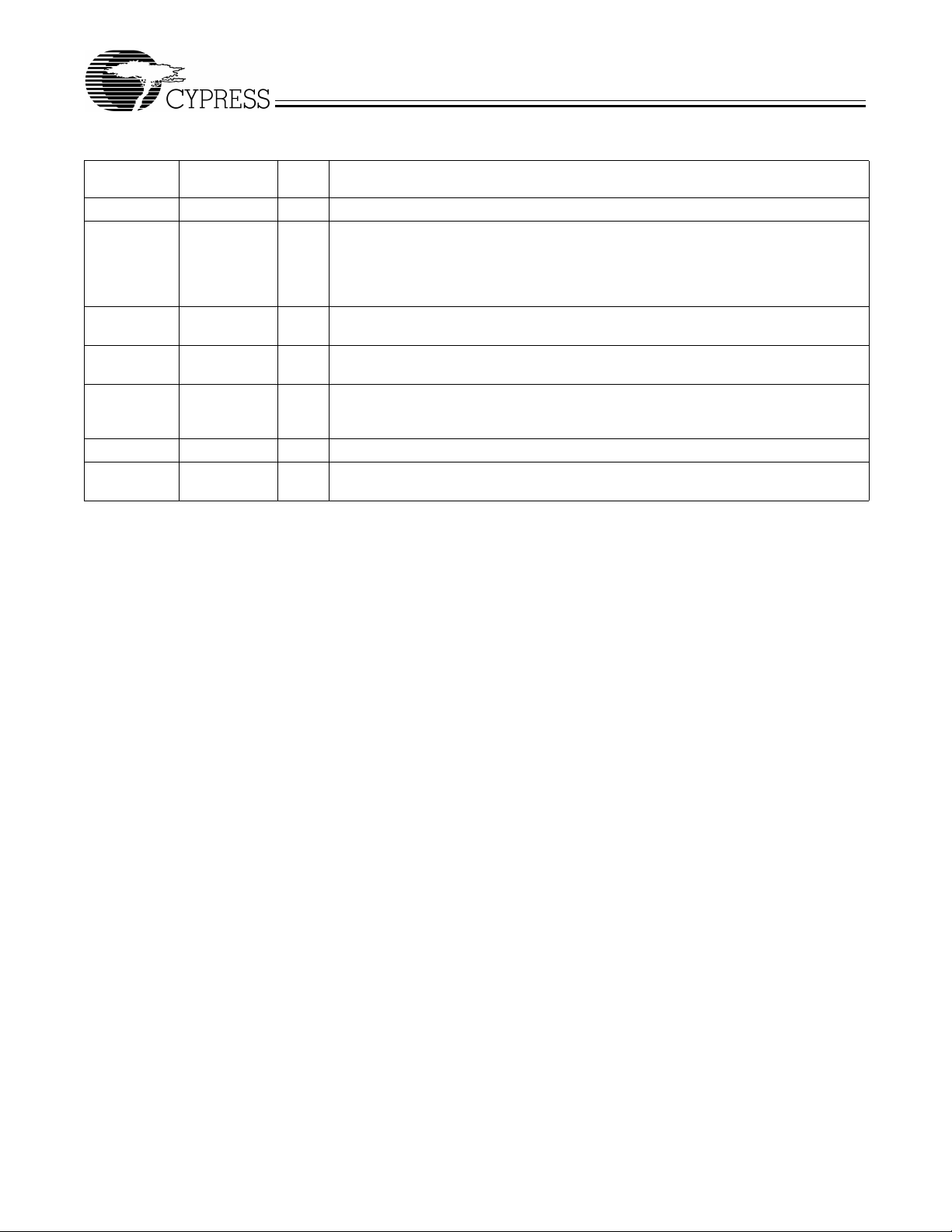
Pin Definitions
Pin Name Pin No.
IN 2 I
FBIN 1 I
OUT1 6 O
OUT2 8 O
VDD 7 P
GND 3 P
FS0:1 4, 5 I
Pin
Type Pin Description
Reference Input:
Feedback Input:
ensure proper func ti onality. If the trac e between FBIN and the output pin being used
for feedback is equal in length to the traces bet ween the outputs and the signal destinations, then t he si gnals re ceiv ed at the dest inations will be synchroni z ed to the REF
signal input (IN).
Output 1:
back signal connected to FBIN, and the FS0:1 inputs (see Table 1).
Output 2:
of OUT1. See Table 1.
Power Connections:
0.1-µF decoupling capacitor. Use ferrite beads to help reduce noise for optimal jitter
performance.
Ground Connection:
Function Select Inputs:
T able 1.
The frequency of the signal provided by this pin is determined by the feed-
The frequency of th e signal provi ded by this pin is one- half of the fr equency
The output signals will be synchronized to this signal.
This input must be fed by one of the outputs (OUT1 or OUT2) to
Connect to 3.3V or 5V. Thi s pi n should be bypassed with a
Connect all grounds to the common system ground plane.
Tie to VDD (HIGH, 1) or GND (LOW, 0) as desired per
W170-01
Overview
The W170-01 is a two-output zero delay buffer and frequency
multiplier. It pro vides an e xternal fee dbac k path all owing maximum flexibility when implementing the Zero Delay feature.
This is explained further in the sec tions of thi s d ata she et ti tle d
“How to Implement Zero Delay,” and “Inserting Othe r D evices
in Feedback Path. ”
The W170-01 is a pin-compatible upgrade of the Cypress
W42C70-01. The W170-01 addresses some application dependent problems experienced by users of the older device.
Most importantly, it addresses the tracking skew problem induced by a reference whic h has Spread Spectrum Timin g enabled on it.
Spread Aware
Many systems being designed n ow utilize a technology called
Spread Spectrum Fr equency Timing Gener ation. Cypress has
been one of the pioneers of SSFTG devel opment , and we designed this product so as not to filter off the Spread Spectrum
feature of the Ref erence input, assu ming it exists. When a zero
delay buffer is not designed to pass the SS feature through,
the result is a significant amount of tracking skew which may
cause problems in systems requiring synchronization.
For more details on Spread Spectrum timing technology,
please see the Cypr ess application note titled, “EMI Suppression Techniques with Spread Spectrum Frequency Timing
Generator (SSFTG) ICs.”
2
Page 3
W170-01
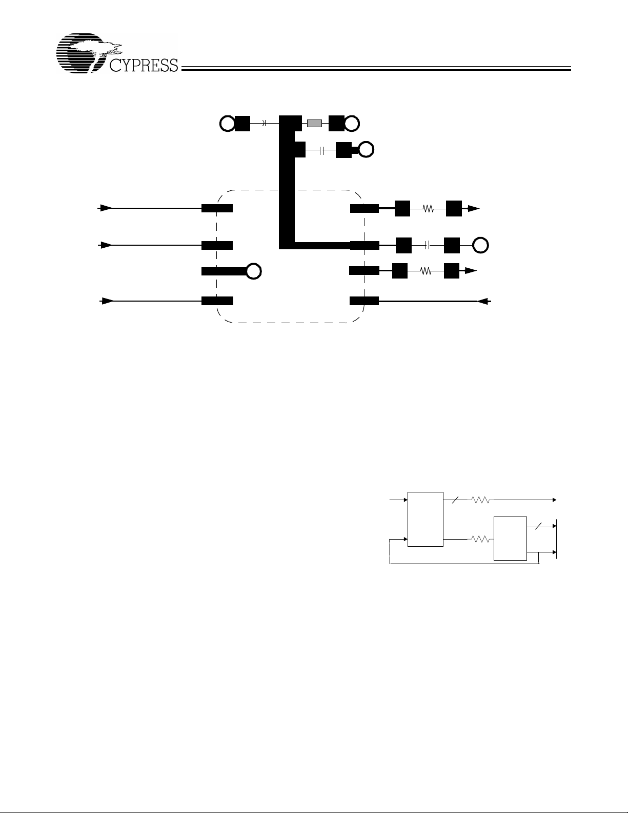
Figure 2. 6 Output Buffer in the Feedback Path
C
A
10 µF
FBIN
IN
GND
1
2
3
G
4
Figure 1. Schematic/Suggested Layout
How to Implement Zero Delay
Typically, zero delay buffers (ZDBs) are used because a designer wants to provide multiple copies of a clock signal in
phase with each other . The whole c oncept be hind ZDBs is that
the signals at the destination chips are all going HIGH at the
same time as the input to the ZDB. In order to achieve this,
layou t must c ompensate f or tra ce length be tween the ZDB an d
the target devices. The method of compensation is described
below.
External feedbac k is the trait that allows f or thi s compensati on.
The PLL on the ZDB will cause the feedback signal to be in
phase with the reference signal. When laying out the board,
match the trace lengths between the output being used for
feed back and the FBIN input to the PLL.
If it is desirable to either add a little delay, or slightly precede
the input signal, this m ay also be affec ted by either making the
trace to the FBIN pin a little shorter or a little longer than the
traces to the devices being clocked.
Ferrite
Bead
C8
0.01 µF
Power Supply Connection
V+G
G
OUT 2
8
V
DD
7
OUT 1
6
5
22
Ω
C9 = 0.1 µF
22
Ω
FS1FS0
OUTPUT 2
G
OUTPUT 1
some other dev ic e. Thi s impl ement ation can be appl ied t o an y
device (ASIC, mul tiple output clock b uffer/driver, etc.) which i s
put into the feedback path.
Referring to Figure 2, if the traces between the ASIC/Buffer
and the destination of the clock signa l(s) (A) are equal in lengt h
to the trace between the buffer and the FBIN pin, the signals
at the destination(s) device will be driven HIGH at the same
time the Reference clock provided to the ZDB goes HIGH.
Synchronizing the other outputs of t he ZDB to the outputs f rom
the ASIC/Buff er is mor e comp le x ho we v er, as a ny pr opaga tion
delay in the ASIC/Buffer must be acco unted for.
Reference
Signal
Zero
Delay
Feedback
Buffer
ASIC/
Buffer
Input
A
Inserti n g Other Devices in Feedback Path
Another nice feature available due to the external feedback is
the ability to synchroniz e signals up to t he signal coming from
3
Page 4
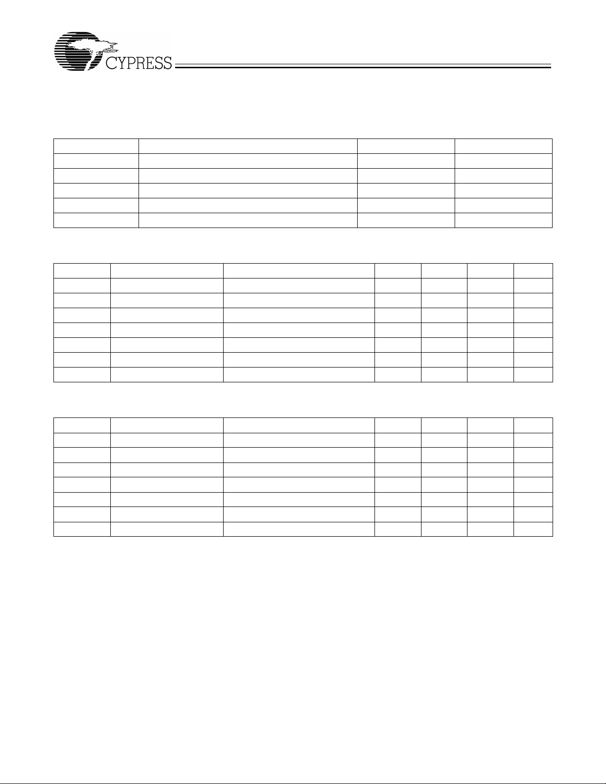
Absolute Maximum Ratings
W170-01
Stresses gre ater th an those li sted i n this tab le may cause permanent damage to the de vice. These represent a stress ratin g
only. Operation of the device at these or any other conditions
.
above those specified in the operating sections of this specification is not implied. Maximum conditions for extended periods may affect reliability.
Parameter Description Rating Unit
V
, V
DD
IN
T
STG
T
A
T
B
P
D
DC Electr i cal C h ar acteristi cs
Voltage on any pin with respect to GND –0.5 to +7 .0 V
Storage Temperature –65 to +150 °C
Operating Temperature 0 to +70 °C
Ambient Temperature under Bias –55 to +125 °C
Power Dissipation 0.5 W
:
=0°C to 70°C, VDD = 3.3V ±5%
T
A
Parameter Description Test Condition Min Typ Max Unit
I
V
V
V
V
I
I
DD
IL
IH
OL
OH
IL
IH
Supply Current Unloaded, 133 MHz 17 35 mA
Input Low Voltage 0.8 V
Input High Voltage 2.0 V
Output Low Voltage IOL = 8 mA 0.4 V
Output High Voltage IOH = 8 mA 2.4 V
Input Low Current VIN = 0V 5 µA
Input High Current VIN = V
DD
5 µA
:
=0°C to 70°C, VDD = 5V ±10%
DC Electr i cal C h ar acteristi cs
T
A
Parameter Description Test Condition Min Typ Max Unit
I
V
V
V
V
I
I
DD
IL
IH
OL
OH
IL
IH
Supply Current Unloaded, 133 MHz 31 50 mA
Input Low Voltage 0.8 V
Input High Voltage 2.0 V
Output Low Voltage IOL = 8 mA 0.4 V
Output High Voltage IOH = 8 mA 2.4 V
Input Low Current VIN = 0V 5 µA
Input High Current VIN = V
DD
5 µA
4
Page 5
W170-01
AC Electrical Characteristics:
TA = 0°C to +70°C, VDD = 3.3V±5%
Paramet er Description T est Condition Min T yp Max Unit
f
IN
f
OUT
t
R
t
F
t
ICLKR
t
ICLKF
t
PD
t
D
t
LOCK
t
JC
Input Frequency
Output Frequency OUT1 20 133 MHz
Output Rise Time 0.8V to 2.0V, 15-pF load 3.5 ns
Output Fall Time 2.0V to 0.8V, 15-pF load 2.5 ns
Input Clock Rise Time
Input Clock Fall Time
FBIN to IN (Reference Input) Skew
Duty Cycle Note 5 405060%
PLL Lock Time Power supply stable 1.0 ms
Jitter, Cycle-to-Cy cle Note 6 200 ps
AC Electrical Characteristics:
[1]
[2]
[2]
OUT2 = REF MHz
[3, 4]
Note 4 300 ps
10 ns
10 ns
TA = 0°C to +70°C, VDD = 5V±10%
Paramet er Description T est Condition Min T yp Max Unit
f
IN
f
OUT
t
R
t
F
t
ICLKR
t
ICLKF
t
PD
t
D
t
LOCK
t
JC
Notes:
1. Input frequency is limited by output frequency range and input to output frequency multiplication factor (which is determined by circuit configuration).
2. Longer input rise and fall time will degrade skew and jitter performance.
3. All AC specifications are measured with a 50Ω transmission line, load terminated with 50Ω to 1.4V.
4. Skew is measured at 1.4V on rising edges.
5. Duty cycle is measured at 1.4V.
6. Jitter is measured on 133-MHz signal at 1.4V.
7. Duty cycle is measured at 1.4V, 120 MHz.
8. Duty cycle at 133 MHz is 35/65 worst case.
Input Frequency
Output Frequency OUT1 20 133 MHz
Output Rise Time 0.8V to 2.0V, 15-pF load 3.5 ns
Output Fall Time 2.0V to 0.8V, 15-pF load 2.5 ns
Input Clock Rise Time
Input Clock Fall Time
FBIN to IN (Reference Input) Skew
Duty Cycle Note 7, 8 40 50 60 %
PLL Lock Time Power supply stable 1.0 ms
Jitter, Cycle-to-Cy cle Note 6 200 ps
[1]
[2]
[2]
OUT2 = REF MHz
[3, 4]
Note 4 300 ps
10 ns
10 ns
Ordering Information
Package
Ordering Code Option
W170 -01 G 8-pin SOIC (150 mil)
Document #: 38-00795
Name
Package Type
5
Page 6
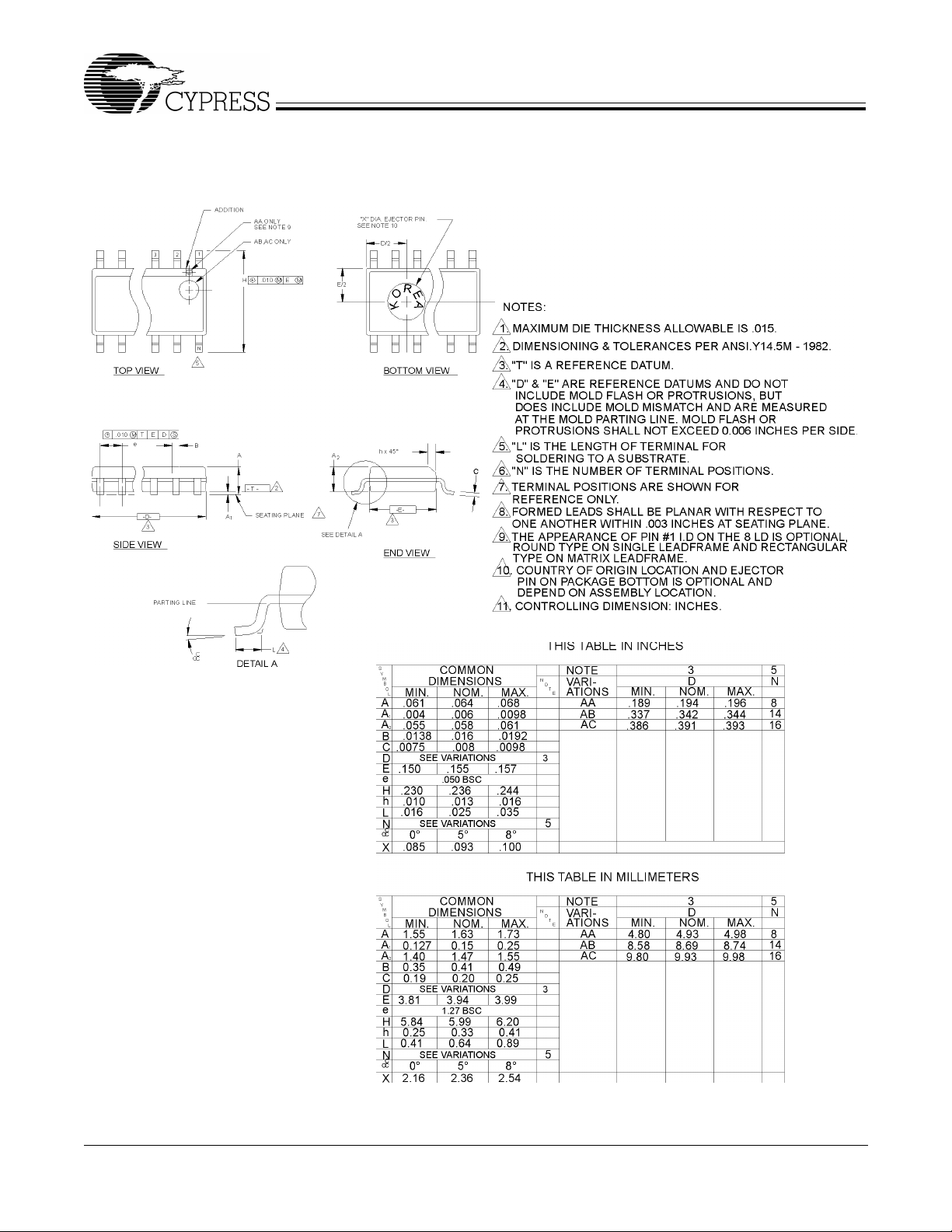
Package Diagram
W170-01
8-Pin Small Outlined Integrated Circuit (SOIC, 150 mil)
© Cypress Semiconductor Corporation, 1999. The information contained herein is subject to change without notice. Cypress Semiconductor Corporation assumes no responsibility for the use
of any circuitry other than circuitry embodied in a Cypress Semiconductor product. Nor does it con vey or imply any lice nse under patent or other rights. Cypress Semicondu ctor does not authorize
its products for use as critical components in life-support systems where a malfunction or failure may reasonably be expected to result in significant injury to the user. The inclusion of Cypress
Semiconductor products in life-support systems application implies that the manufacturer assumes all risk of such use and in doing so indemnifies Cypress Semiconductor against all charges.
 Loading...