

Page 1
W210
Spread Spectrum FTG for VIA K7 Chipset
Features
• Maximized EMI Suppression usi ng Cypress’s Spread
Spec trum te chnol ogy
• Single-chi p system frequency synthesizer for VIA K7
chipset
• One pair of different ial CPU outputs for K7 Processor
• One open-drain CPU output for VIA K7 chips et
• Six copies of PCI output
• One 48-MHz output for USB
• One 24-MHz or 48-MHz output for SIO
• T wo buffered reference outputs
• Thirteen SDRAM outputs provide support for 3 DIMMs
• Supports frequencies up to 200 MHz
2
•I
C™ interface for programming
• Power man agement control inputs
• Available in 48-pin SSOP
Key Specific ati o n s
CPU to CPU Output Skew:.... .. ................................... 175 ps
PCI to PCI Output Skew:...................... ...................... 500 ps
: .................................................................... 3.3V±5%
V
DDQ3
T able 1. Mode Input Table
Mode Pin 2
0 CPU_STOP#
1REF0
T able 2. Pin Selectable Fre quency
Input Address
CPU
(MHz)
PCI0:5
(MHz)
Spread
SpectrumFS3 FS2 FS1 FS0
1 1 1 1 133.3 33.3 ±0.5%
1 1 1 0 75 37.5 ±0.5%
1 1 0 1 100.2 33.3 ±0.5%
1 1 0 0 66.8 33.4 ±0.5%
1 0 1 1 79 39.5 OFF
1 0 1 0 110 36.7 OFF
1 0 0 1 115 38.3 OFF
1 0 0 0 120 30 OFF
0 1 1 1 133.3 33.3 OFF
0 1 1 0 83.3 27.7 OFF
0 1 0 1 100.2 33.3 OFF
0 1 0 0 66.8 33.4 OFF
0 0 1 1 124 31.0 OFF
0 0 1 0 129 32.3 OFF
0 0 0 1 138 34.5 OFF
0 0 0 0 143 35.8 OFF
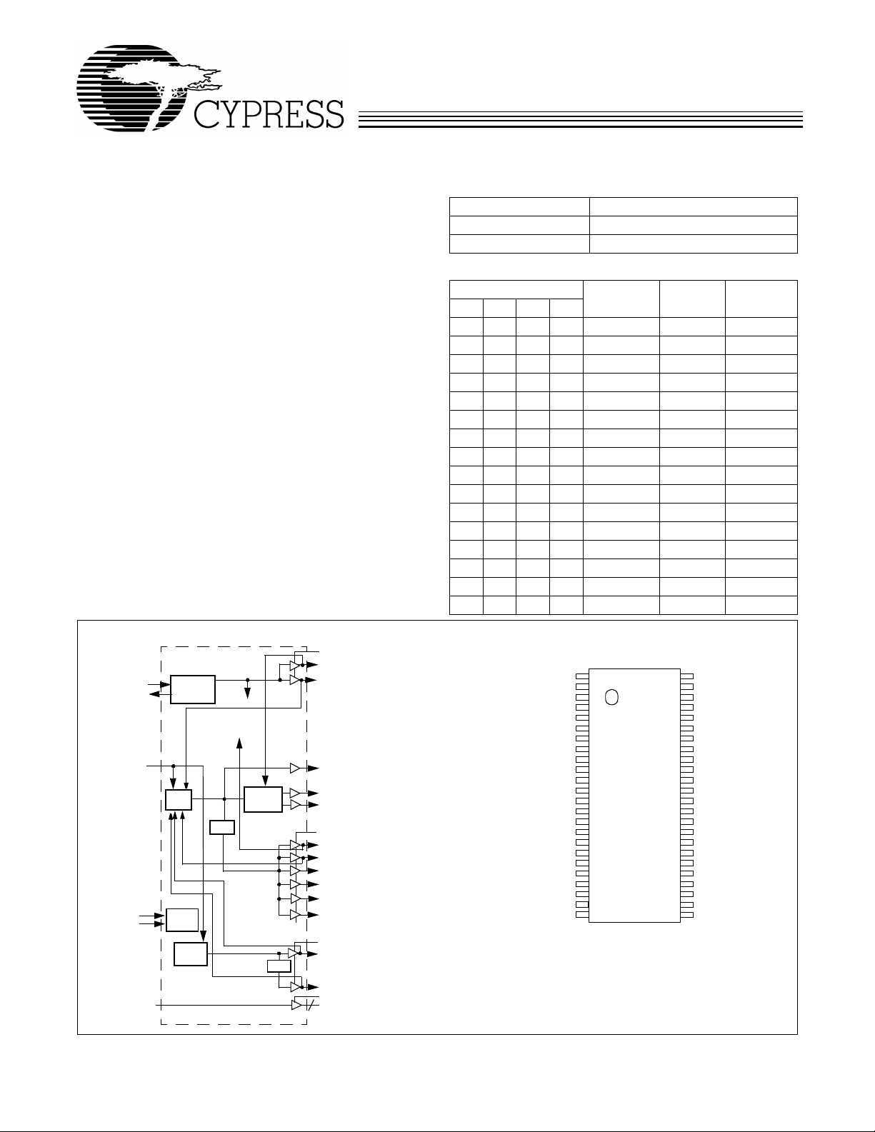
Block Diagram
X1
X2
PWRDWN#
SDA TA
SCLK
SDRAMIN
I2C is a trademark of Philips Corporation.
PLL 1
I2C
Logic
PLL2
XTAL
OSC
÷2,3,4
PLL Ref Freq
I/O Pin
Control
Control
Stop
Clock
Pin Configuration
VDDQ3
REF0/(CPU_STOP#)
REF1/FS0
CPUT_CS
CPUT0
CPUC0
VDDQ3
PCI0/MODE
PCI1/FS1
PCI2
PCI3
PCI4
PCI5
VDDQ3
÷2
48MHz/FS2
24_48MHz/FS3
VDDQ3
SDRAM0:12
13
REF0/(CPU_STOP#)
Note:
1. Internal pull-up resistors should not be relied upon for setting I/O
VDDQ3
GND
X1
X2
VDDQ3
PCI0/MODE
PCI1/FS1*
GND
PCI2
PCI3
PCI4
PCI5
VDDQ3
SDRAMIN
GND
SDRAM11
SDRAM10
VDDQ3
SDRAM9
SDRAM8
GND
SDA TA
I2C
{
SCLK
pins HIGH. Pin function with parentheses determined by MODE pin
resistor strapping. Unlike other I/O pins, input FS3 has an internal
pull-down resistor.
[1]
REF1/FS0*
W210
48
GND
47
CPUT_CS
46
GND
45
44
CPUC0
43
CPUT0
VDDQ3
42
41
PWRDWN#*
SDRAM12
40
GND
39
SDRAM0
38
SDRAM1
37
VDDQ3
36
SDRAM2
35
SDRAM3
34
GND
33
SDRAM4
32
SDRAM5
31
VDDQ3
30
SDRAM6
29
SDRAM7
28
VDDQ3
27
48MHz/FS2*
26
24_48MHz/FS3^
25
1
2
3
4
5
6
7
8
9
10
11
12
13
14
15
16
17
18
19
20
21
22
23
24
Cypress Semiconductor Corporation
• 3901 North First Street • San Jose • CA 95134 • 408-943-2600
April 11, 2000, rev. *C
Page 2
Pin Definitions
Pin Name Pin No. Pin Type Pin Description
CPUT0,
CPUC0,
CPUT_CS
PCI2:5 10, 11, 12, 13 O
PCI1/FS1 8 I/O
PCI0/MODE 7 I/O
PWRDWN# 41 I
48MHz/FS2 26 I/O
24_48MHz/
FS3
REF1/FS0 48 I/O
REF0/
CPU_STOP#
SDRAMIN 15 I
SDRAM0:12 38, 37, 35,
SCLK 24 I Clock pin for I
SDATA 23 I/O Data pi n for I
X1 4 I
X2 5 I
VDDQ3 1, 6, 14, 19,
GND 3, 9, 16, 22,
43, 44, 46 O
(open-
drain)
25 I/O
2 I/O
O
34, 32, 31,
29, 28, 21,
20, 18, 17, 40
P
27, 30, 36, 42
G
33, 39, 45, 47
CPU Clock Output 0:
for the K7 proc essor. CPUT_CS is the open-drain cl ock output for the chips et. It
has the same phase relat ionship as CPUT0.
PCI Clock Outpu ts 2 through 5:
the PWRDWN# control pin. Frequency is set by FS0:3 inputs or through serial
input interface, see Tables 2 and 6 for details. Output voltage swing is controlled
by volt age applied to VDDQ3.
Fixed PCI Clo ck Output/Frequency Select 1:
FS0:3 inputs or through serial input interface. This output is controlled by the
PWRDWN# input. This pin also serves as a power-on strap opt ion to determine
device operating frequency as describe d in Table 2.
Fixed PCI Cloc k Output/Mode:
or through serial inp u t i nterface, see Tables 2 and 6. This output is controlled by
the PWRDWN# input. This pin also serves as a power -on strap option to determine
the function of pin 2, see Table 1 for details.
PWRDWN# Input :
mode when held LOW. In power-down mode,CPUC0 will be three-stated and all
the other output clocks will be driven LOW.
48-MHz Output/Fr equency Se lec t 2:
standard PC systems, this output can be used as the reference for the Uni versal
Serial Bus host control ler. This pin also serves as a power-on strap option to
determine device operating frequency as desc ribe d in Table 2.
24_48-MHz Outpu t/Frequency Sel ect 3:
be used as the clock input f or a Super I/O chip . The output frequency is controlled
by Configur ation Byte 3 bit[6]. The defaul t out put frequency is 24 MHz. This pin
also serves as a power -on strap option to determine device operating frequency
as described in Table 2.
Reference Cloc k Output 1/Frequency Sel ect 2:
This pin also serves as a power-on strap option to dete rmine device operating
frequency as described in Table 2. Upon power-up, FS0 input will be latched, which
will set clock frequencies as described in Table 2.
Reference Cloc k Output 0 or CPU_STOP# Input Pin:
by the MODE pin. When CPU_ST OP# inp ut is asse rted LOW, it will drive CPUT0
and CPUT_CS to l ogic 0, and it will three -state CPUC0. When this pin i s configured
as an output, this pin becom es a 3.3V 14. 318-MHz output clock.
Buffered Input Pin:
(SDRAM0:12).
Buffered Outputs:
provided at the SDRAMIN input. The swing is set by VDDQ3, and they are deactivated when PWRDWN# input is set LOW.
2
C circuitry.
2
C circuitry .
Crystal Connection or Ext ernal Ref erence Frequenc y Input:
functions . It can be used as an external 14.318-MHz crystal con nection or as an
external reference frequency input.
Crystal Connection:
using an external reference, this pin must be left unconnected.
Power Connection:
PCI outputs, ref erence outp uts, 48-MHz ou tput, and 24_4 8-MHz ou tpu t. Connect
to 3.3V supp ly.
Ground Connections:
plane.
CPUT0 and CPUC0 are the differ ential CPU cl oc k output s
These four PCI clock outputs are controlled by
As an output, frequency is set by the F S0:3 inputs
LVTTL-compatibl e inpu t that place s t he de vi ce in po we r-do wn
48 MHz is provi ded in normal operat ion. In
The signal pr ovide d t o this input pin i s buf f ere d to 13 outp uts
These thirteen d edicat ed outpu ts prov ide cop ies of t he sig nal
An input connection for an external 14.318-MHz crystal. If
Power supply for core logic, PLL circuitry, SDRAM outputs,
Connect all ground pins to the common system ground
W210
As an output, frequency is set by
In standard PC systems, th is output can
3.3V 14.318-MHz output clock.
Function is determined
This pin has dual
2
Page 3
W210
Overview
The W210 was developed as a single-chip device to meet the
clockin g needs of VIA K7 c ore logic chi p sets. I n addition t o the
typical ou tputs provided by a standard FTG, the W210 adds a
thirteenth output buff er, supporting SDRAM DIMM modules in
conjunction with the chipset.
Cypress’s proprietary spread spectrum frequency synthesis
technique is a feature of the CPU and PCI outputs. When enabled, th is feat ure reduces the peak EMI measurement s of not
only the output signals and their harmonics, but also of any
other clock signals that are properly synchr onized to them.
Functional Description
I/O Pin Operation
Pins 7, 8, 25, 26, and 48 are dual-purpose l/O pins. Upon
power-up these pins act as logic inputs, allowing the determination of assigned device functions. A short time after powerup, the logic state of each pin is latched and the pins becom e
clock outputs. This feature reduces device pin count by combining cloc k outputs with input select pins .
An external 10-kΩ “strapping” resistor is connected between
the l/O pin and ground or V
latch to “0,” connection to V
Figure 2 show two suggested methods for strapping resistor
connections.
. Connection to ground sets a
DD
sets a latch to “1.” Fig ure 1 an d
DD
Upon W210 power-up, the first 2 ms of operation is used for
input logic selection. During this period, the five I/O pin s (7, 8,
25, 26, 48) are three-stated, allowing the output strapping resistor on the l/O pins to pull the pins and their associated capacitiv e clock load to either a logic HIGH or LOW state. At the
end of the 2-ms period, the established logic “0” or “1” condition of the l/O pin is latched. Next the output buffer is enabl ed
converting t he l/O pins into operating clock outputs. The 2-ms
timer starts w hen V
be reset by turning V
reaches 2.0V. The input bits can only
DD
off and then back on again.
DD
It should be noted that the strapping resistors have no significant effect on clock output signal integrity. The drive impedance of clock outputs is <40Ω (nominal), which is minimally
affected by the 10-kΩ strap to ground or V
ries termination resistor, the output strapping resistor should
. As with the se-
DD
be placed as close to the l/O pin as possible in order to keep
the interconnecting trace short. The trace from the resistor to
ground or V
should be ke pt less t han tw o i nches i n lengt h t o
DD
prevent system noise coupling during input l ogic sampling.
When the clock outputs are enabled following the 2-ms input
period, the specified output frequency is delivered on the pin,
assuming that V
full value , output frequency initi ally ma y be belo w target b ut will
increase to target once V
case, a shor t output clock cycle may be produced from the
has stabilized. If VDD has not yet reached
DD
voltage has stabilized. In either
DD
CPU clock outputs when the outputs are enabled.
V
DD
Output Stra pp i ng Resi st or
W210
Power-on
Reset
Timer
W210
Power-on
Reset
Timer
10 k
Output Three -state
Output
Buffer
Hold
Output
Low
QD
Data
Latch
(Load Option 1)
(Load Option 0)
10 k
Ω
Ω
Figure 1. Input Logic Selection Through Resistor Load Option
Jumper Options
V
DD
10 k
Ω
Output
Buffer
Output Three -state
Hold
Output
Low
QD
Data
Latch
Resistor Value R
Series Termination Resistor
R
Output Stra pp i ng Resi st or
Series Termination Resistor
R
Clock Load
Clock Load
Figure 2. Input Logic Selection Through Jumper Option
3
Page 4
W210
Spread Spectrum Frequency Tim ing G enera to r
The device generates a clock that is frequency modulated in
order to increase the bandwidth that it occu pies. By increas ing
the bandwidth of the fundamental and its harmonics, the amplitudes of the radiated electromagnetic emissions are reduced. This effect is depicted in Figure 3.
As shown in Figure 3, a harmonic of a modulated clock has a
much low er amplitu de than that of an un modulated si gnal. The
reduction in amplitude is dependent on the harmonic number
and the frequency deviation or spread. The equation for the
reduction is:
dB = 6.5 + 9*log
(P) + 9*log10(F)
10
Amplitude (dB)
5 dB/d iv
SSFTG Ty p ic al Clock
Where P is the percenta ge of de vi ation and F is the frequen cy
in MHz where the reduction is measured.
The output clock is modulated with a waveform depicted in
Figure 4. This waveform, as discussed in “Spread Spectrum
Clock Generation f or the Reducti on of Radiated Emissio ns” by
Bush, Fessler, and Hardin produces the maximum reduction
in the amplitude of radiated electromagnetic emissions. The
deviati on select ed for this chi p is speci fied in Table 6. Figure 4
details the Cypress spr eading pat tern. Cypres s does off er options with more spread and greater EMI reduction. Contact
your local Sales representative for details on these devices.
Spread Spectrum clocking is activated or deactivated by selecting the appropriate v al ues fo r bits 1–0 in data byte 0 of the
2
I
C data stream. Refer to Table 6 for more details.
-SS %
Frequency S pan (MHz)
+SS%
Figure 3. Clock Harmonic with and without SSCG Modulation Frequency Domain Representation
MAX (0%)
10%
20%
30%
40%
50%
60%
70%
80%
FREQUENCY
MIN (–0.5%)
90%
100%
10%
20%
30%
40%
50%
60%
70%
80%
90%
Figure 4. Typica l Modulation Profile
100%
4
Page 5
W210
Serial Data Interface
The W210 features a two-pin, serial data interface that can be
used to configure internal register settings that control particular de vice funct ions. Upon po wer-up , the W210 i nitiali zes wit h
default register settings, therefore the use of this serial data
interface is optional. The serial interface is write-only (to the
clock chi p) and i s the dedi cated f unc tion of de v ice pi ns SDA TA
and SCLOCK. In motherboard applications, SDATA and
SCLOCK are typically driven by two logic outputs of the
T able 3. Serial Data Interface Control Functions Summary
Control Function Description Common Application
Clock Output Disable Any individual clock output(s) can be disabled. Dis-
CPU Clock Frequency
Selection
Spread Spectrum
Enabling
Output Three-state Puts clock output into a high imped ance state. Production PCB testing.
(Reserved) Reserved functio n for future device r evision or pro-
abled outputs ar e actively held LOW.
Provides CPU/PCI frequency selections through
software. Frequency is changed in a smooth and
controlled fashion.
Enables or disables spread spectrum clocking. For EMI reduction.
duc tion devi c e testi n g.
chipset. Clock device register changes are normally made
upon system initialization, if any are required. The interface
can also be used during system operation for power management functions. Tabl e 3 summarizes the control functions of
the serial data interface.
Operation
Data is written to the W210 in elev en bytes of eight bits each.
Bytes are written in the order shown in Table 4.
Unused outputs are di sabled to reduce EMI
and system power. Examples are clock outputs to unused PCI slots.
For alternate microprocessors and power
management options . Smooth freque ncy transition allows CPU frequency change under
normal system operati on.
No user applicat ion. Regist er bit must be wri tten as 0.
Table 4. Byte Writing Sequence
Byte Sequence Byte Name Bit Sequence Byte Description
1 Slave Address 11010010 Commands the W210 to accept the bits in Data Bytes 0–6 for internal
register configuration. Since other devices may exist on the same com mon serial data b us , it is neces sary to ha v e a speci fic s lav e address for
each potential receiver. The slave receiver address for the W210 is
11010010. Register sett ing will not be made if t he Slav e Address is not
correct (or is for an alternate slave recei ver).
2 Command
Code
3 Byte Count Don’t Care Unused by the W210, therefore bit values are ignored (“Don’t C a re”).
4 Data Byte 0 Refer to Ta ble 5 The data bits in Dat a Bytes 0 –7 set internal W 210 regi sters that co ntrol
5 Data Byte 1
6 Data Byte 2
7 Data Byte 3
8 Data Byte 4
9 Data Byte 5
10 Data Byte 6
11 Data Byte 7
Don’t Care Unused by the W210, therefore bit values are ignored (“Don’t Care”).
This byte m ust be inclu ded in the dat a write sequence to maintain pro per
byte allocatio n. The Command Code Byte is part of the standard serial
communication protocol and may be used when writing to another addressed slave receiver on the serial data bus.
This byte m ust be inclu ded in the dat a write sequence to maintain pro per
byte alloc ati on. The Byte Count Byte is part of the standard serial communication pr otocol and may be used wh en writing to another address ed
slave receiver on the serial data bus.
device operation. The data bits are only accept ed when the Address
Byte bit sequence is 11010010, as noted above. F or description of bit
control functions, refer to Table 5, Data Byte Serial Configuration Map.
5
Page 6

W210
Writin g D a ta Bytes
Each bit in the data bytes controls a particular device function
except f o r the “reserved” bits, which must be writt en as a logic
0. Bits are written MSB (most significant bit) first, which is bit
Table 5. Data Bytes 0–7 Serial Configuration Map
Affected Pin
Bit(s)
Data Byte 0
7 -- -- (Reserved) -- -- 0
6 -- -- SEL_2 See Table 6 0
5 -- -- SEL_1 See Table 6 0
4 -- -- SEL_0 See Table 6 0
3 -- -- Hardware/Software Frequency
2 -- -- SEL_4 See Table 6 1
1 -- -- SEL_3 See Table 6 0
0 -- -- (Reserved) Normal Three-stated 0
Data Byte 1
7 -- -- (Reserved) -- -- 0
6 -- -- (Reserved) -- -- 0
5 -- -- (Reserved) -- -- 0
4 -- -- (Reserved) -- -- 0
3 -- -- (Reserved) Write to ‘1’ -- -- 1
2 -- -- (Reserved) Write to ‘1’ -- -- 1
1 -- -- (Reserved) Write to ‘1’ -- -- 1
0 -- (Reserved) Write to ‘1’ -- -- 1
Data Byte 2
7 -- -- (Reserved) -- -- 0
6 7 PCI0 Clock Output Disable Low Active 1
5 -- -- (Reserved) -- -- 0
4 13 PCI5 Clock Output Disable Low Active 1
3 12 PCI4 Clock Output Disable Low Active 1
2 11 PCI3 Clock Output Disable Low Active 1
1 10 PCI2 Clock Output Disable Low Active 1
0 8 PCI1 Clock Output Disable Low Active 1
Data Byte 3
7 -- -- (Reserved) -- -- 0
6 -- SEL_48MHz SEL_48MHz as the output fre-
5 26 48MHz Clock Output Disable Low Active 1
4 25 24_48MHz Clock Output Disable Low Active 1
3 -- -- (Reserved) -- -- 0
2 21, 20,
18, 17
SDRAM8:11 Clock Output Disable Low Active 1
Control Function
Select
quency for 24_48MHz
7. Ta b l e 5 gives the bit form ats for registers located in Data
Bytes 0–7.
Ta ble 6 details additional frequency selections that are available through th e seria l dat a interface.
Bit Control
Hardware Software 0
24 MHz 48 MHz 0
DefaultPin No. Pin Name 0 1
6
Page 7

W210
Table 5. Data Bytes 0–7 Serial Configuration Map
Affected Pin
Bit(s)
1 32, 31,
29, 28
0 38, 37,
35, 34
Data Byte 4
7 -- -- (Reserved) -- -- 0
6 -- -- (Reserved) -- -- 0
5 -- -- (Reserved) -- -- 0
4 -- -- (Reserved) -- -- 0
3 -- -- (Reserved) -- -- 0
2 -- -- (Reserved) -- -- 0
1 -- -- (Reserved) -- -- 0
0 -- -- (Reserved) -- -- 0
Data Byte 5
7 -- -- (Reserved) -- -- 0
6 -- -- (Reserved) -- -- 0
5 -- -- (Reserved) -- -- 0
4 -- -- (Reserved) -- -- 1
3 -- -- (Reserved) -- -- 0
2 -- -- (Reserved) -- -- 0
1 48 REF1 Clock Output Disable Low Active 1
0 2 REF0 Clock Output Disable Low Active 1
Data Byte 6
7 -- -- (Reserved) -- -- 0
6 -- -- (Reserved) -- -- 0
5 -- -- (Reserved) -- -- 0
4 -- -- (Reserved) -- -- 0
3 -- -- (Reserved) -- -- 0
2 -- -- (Reserved) -- -- 0
1 -- -- (Reserved) -- -- 0
0 -- -- (Reserved) -- -- 0
Data Byte 7
7 -- -- (Reserved) -- -- 0
6 -- -- (Reserved) -- -- 0
5 -- -- (Reserved) -- -- 0
4 -- -- (Reserved) -- -- 0
3 -- -- (Reserved) -- -- 0
2 -- -- (Reserved) -- -- 0
1 -- -- (Reserved) -- -- 0
0 -- -- (Reserved) -- -- 0
SDRAM4:7 Clock Output Disable Low Active 1
SDRAM0:3 Clock Output Disable Low Active 1
Control Function
(continued)
Bit Control
DefaultPin No. Pin Name 0 1
7
Page 8

T able 6. Additional Frequency Selections through Serial Data Interface Data Bytes
Input Conditions Output Frequency
Data Byte 0, Bit 3 = 1
Bit 2
SEL_4
1 1 1 1 1 133.3 33.3 ±0.5%
1 1 1 1 0 75 37.5 ±0.5%
1 1 1 0 1 100.2 33.3 ±0. 5%
1 1 1 0 0 66.8 33.4 ±0.5%
11011 79 39.5 OFF
1 1 0 1 0 110 36.7 OFF
1 1 0 0 1 115 38.3 OFF
11000 120 30 OFF
10111 133.3 33.3 OFF
1 0 1 1 0 83.3 27.7 OFF
10101 100.2 33.3 OFF
1 0 1 0 0 66.8 33.4 OFF
1 0 0 1 1 124 31.0 OFF
1 0 0 1 0 129 32.3 OFF
1 0 0 0 1 138 34.5 OFF
1 0 0 0 0 143 35.8 OFF
01111 85 28.3 OFF
0 1 1 1 0 87.5 29.2 OFF
01101 90 30 OFF
0 1 1 0 0 92.5 30.8 OFF
01011 95 31.7 OFF
0 1 0 1 0 147 36.8 OFF
0 1 0 0 1 152 30.4 OFF
0 1 0 0 0 154 30.8 OFF
0 0 1 1 1 157 31.4 OFF
0 0 1 1 0 159 31.8 OFF
0 0 1 0 1 162 32.4 OFF
0 0 1 0 0 166 33.2 OFF
0 0 0 1 1 171 34.2 OFF
00010 180 36 OFF
00001 190 38 OFF
00000 200 40 OFF
Bit 1
SEL_3
Bit 6
SEL_2
Bit 5
SEL_1
Bit 4
SEL_0
CPU PCI Spread Spectrum
W210
8
Page 9

Absolute Maximum Ratings
W210
Stresses gre ater th an those li sted i n this tab le may cause permanent damage to the de vice. These represent a stress ratin g
only. Operation of the device at these or any other conditions
.
above those specified in the operating sections of this specification is not implied. Maximum conditions for extended periods may affect reliability.
Parameter Description Rating Unit
V
, V
DD
IN
T
STG
T
B
T
A
ESD
PROT
DC Electr i cal C h ar acteristics:
Voltage on any pin with respect to GND –0.5 to +7 .0 V
Storage Temperature –65 to +150 °C
Ambient Temperature under Bias –55 to +125 °C
Operating Temperature 0 to +70 °C
Input ESD Protection 2 (min.) kV
TA = 0°C to +70°C, V
DDQ3
= 3.3V±5%
Parameter Description Tes t Condi tion Min. Typ. Max. Unit
Supply Current
I
I
DD
DD
3.3V Supply Current C PUT0, CPUC0,
CPU_CS =100 MHz
Outputs Loaded
2.5V Supply Current C PUT0, CPUC0,
CPU_CS =100 MHz
Outputs Loaded
260 mA
[2]
25 mA
[2]
Logic Inputs
V
IL
V
IH
I
IL
I
IH
Input Low V oltage GND – 0.3 0.8 V
Input High V oltage 2.0 VDD + 0.3 V
Input Low Current
Input High Current
[3]
[3]
–25 µA
10 µA
Clock Outputs
V
OL
V
OH
V
OL
Output Low Voltage I
Output High Voltage IOH = –1 mA 3.1 V
Output Low Voltage CPUT_CS,
CPUT0, CPUC0
V
OH
I
OL
Output High Voltage CPUT_CS,
CPUT0, CPUC0
Output Low Current PCI0:5 VOL = 1.5V 70 110 135 mA
REF0:1 V
48 MHz V
24 MHz V
SDRAM0:12 V
I
OH
Output H igh Current PCI0:5 V
REF0:1 V
48 MHz V
24 MHz V
SDRAM0:12 V
Notes:
2. All clock outputs loaded with 6" 60Ω transmission lines with 22-pF capacitors.
3. W210 logic inputs (except FS3) have internal pull-up devices (pull-ups not full CMOS level). Logic input FS3 has an internal pull-down device.
= 1 mA 50 mV
OL
Termination to V pull-up
00.3V
(external)
Termination to V pull-up
1.0 1.2 V
(external)
= 1.5V 50 70 100 mA
OL
= 1.5V 50 70 100 mA
OL
= 1.5V 50 70 100 mA
OL
= 1.5V 70 110 135 mA
OL
= 1.5V 70 110 135 mA
OH
= 1.5V 50 70 100 mA
OH
= 1.5V 50 70 100 mA
OH
= 1.5V 50 70 100 mA
OH
= 1.5V 70 110 135 mA
OH
9
Page 10

W210
DC Electr i cal C h ar acteristics:
TA = 0°C to +70°C, V
= 3.3V±5% (continued )
DDQ3
Parameter Description Tes t Condi tion Min. Typ. Max. Unit
Crystal Oscillator
[6]
[4]
V
= 3.3V 1.65 V
DDQ3
14 pF
Pin X2 unconnected 28 pF
V
TH
C
C
LOAD
IN,X1
X1 Input Threshold Voltage
Load Capacitance, Imposed on
External C rys tal
[5]
X1 Input Capacitance
Pin Capacitance/Inductance
C
IN
C
OUT
L
IN
AC Electrical Characteristics
T
= 0°C to +70°C, V
A
Input Pin Capacitance Except X1 and X2 5 pF
Output Pin Capacitance 6 pF
Input Pin Inductance 7nH
= 3.3V±5%
DDQ3
AC clock parameters are tested and guaranteed over stated operating conditions using the stated lump capacitive load at the
clock o utput; S pr ead Sp ec trum is disabled .
CPU Clock Outputs (CPUT0, CPUC0, CPUT_CS)
[7]
CPU = 100 MHz CPU = 133 MHz
Parameter Description Test Condition/Comments
t
R
t
F
t
D
t
JC
f
ST
Output Rise Edge Rate 1.0 1.0 V/ns
Output Fall Edge Rate 1.0 1.0 V/ns
Duty Cycle Measured at 50% point 50 50 %
Jitter, Cycle to Cycle 250 250 ps
Fre quency Stabilization
from P ower-up (cold
start)
Assumes full supply v oltage reached
within 1 ms from power-up. Short
cycles exist prior to frequency
33ms
UnitMin. Typ. Max. Min. Typ. Max.
stabilization.
Z
o
Notes:
4. X1 input threshold voltage (typical) is V
5. The W210 contains an internal crystal load capacitor between pin X1 and ground and another between pin X2 and ground. Total load placed on crystal is 14 pF;
this includes typical stray capacitance of short PCB traces to crystal.
6. X1 input capacitance is applicable when driving X1 with an external clock source (X2 is left unconnected).
7. Refer to
AC Output Impe dance VO = V
/2.
DD
for K7 operation clock driver test circuit.
Figure 5
X
50 50 Ω
10
Page 11

W210
PCI Clock Outputs, PCI0:5 (Lump Capacitance Test Load = 30 pF
Parameter Description Test Condition/Comments Min. Typ. Max. Unit
t
P
t
H
t
L
t
R
t
F
t
D
t
JC
t
SK
t
O
f
ST
Z
o
REF0:1 Clock Outputs (Lump Capacitance Test Load = 20 pF)
Parameter Description Test Condition/Comments Min. Typ. Max. Unit
f Frequency, Actual Frequency generated by crystal oscillator 14.318 MHz
t
R
t
F
t
D
f
ST
Z
o
Period Measured on rising edge at 1.5V 30 ns
High Time Duration of clock cycle above 2.4V 12 ns
Low Time Duration of clock cycle below 0.4V 12 ns
Output Rise Edge Rate Measured from 0.4V to 2.4V 1 4 V/ns
Output Fall Edge Rate Measured from 2.4V to 0.4V 1 4 V/ns
Duty Cycle Measured on rising and falling edge at 1.5V 45 55 %
Jitter , Cycle-to-Cycle Measured on rising edge at 1.5V. Maximum
250 ps
differ ence of cyc le time be tween tw o adjacent cycles .
Output Skew Measu red on ri sing edge at 1.5V 500 ps
CPU to PCI Clock Skew Covers all CPU/PCI outputs. Measured on rising
1.5 4 ns
edge at 1.5V. CPU leads PCI output.
Freque ncy Stabilization
from Power-up (cold
start)
AC Output Impeda nce Average val ue duri ng switching transition. Used for
Assumes full supply voltage reached within 1 ms
from power-up. Short cycles exist prior to frequen cy
stabilization.
3ms
30 Ω
determining series termination value.
Output Rise Edge Rate Measured from 0.4V to 2.4V 0.5 2 V/ns
Output Fall Edge Rate Measured from 2.4V to 0.4V 0.5 2 V/ns
Duty Cycle Measured on rising and falling edge at 1.5V 45 55 %
Freque ncy Stabilization from
Power-up (cold start)
Assumes full supply voltage reached within
1 ms from power-up. Short cycles exi st prior to
3ms
frequency stabi li zation.
AC Output Impedance Ave rage value duri ng switchi ng transition. Used
40 Ω
for determining seri es termination value.
48-MHz Clock Output (Lump Capacit ance Test Load = 20 pF)
Parameter Description Test Condition/Comments Min. Typ. Max. Unit
f Frequency, Actual Determined by PLL divider ratio (see m/n below) 48.008 MHz
f
D
Deviation from 48 MHz (48.008 – 48)/48 +167 ppm
m/n PLL Ratio (14.31818 MHz x 57/17 = 48.008 MHz) 57/17
t
R
t
F
t
D
f
ST
Output Rise Edge Rate Measured from 0.4V to 2.4V 0.5 2 V/ns
Output Fall Edge Rate Measured from 2.4V to 0.4V 0.5 2 V/ns
Duty Cycle Measured on rising and falling edge at 1.5V 45 55 %
Freque ncy Stabilization
from Power-up (cold start)
Assumes full supply vol tage reached wit hin 1 ms
from power-up. Short cycles exist prior to fre-
3ms
quency stabilization.
Z
o
AC Output Impedance Average value during switching transition. Used
for determining seri es termination value.
40 Ω
11
Page 12

W210
24-MHz Clock Output (Lump Capacit ance Test Load = 20 pF)
Parameter Description Test Condition/Comments Min. Typ. Max. Unit
f Frequency, Actual Determined by PLL divider ratio (see m/n below) 24.004 MHz
f
D
m/n PLL Ratio (14.31818 MHz x 57/34 = 24.004 MHz) 57/34
t
R
t
F
t
D
f
ST
Z
o
Deviation from 24 MHz (24.004 – 24)/24 +167 ppm
Output Rise Edge Rate Measured from 0.4V to 2.4V 0.5 2 V/ns
Output Fall Edge Rate Measured from 2.4V to 0.4V 0.5 2 V/ns
Duty Cycle Measured on rising and falling edge at 1.5V 45 55 %
Freque ncy Stabilization
from Power-up (cold start)
Assumes full supply vol tage reached wit hin 1 ms
from power-up. Short cycles exist prior to fre-
3ms
quency stabilization.
AC Output Impedance Average value during switching transition. Used
40 Ω
for determining seri es termination value.
1.5V
R1
68
”
20p
CPUCLK_T
Ω
Z0 = 52
Length = 5”
R8
47
T1
Z0 = 52
Length = 3
T2
Ω
Cl
pp
ip
Clock Chip
CPU
Driver
CPUCLK_C
R9
47
Figure 5. K7 Open Drain Clock Driver T est Circuit
Ordering Information
Package
Ordering Code
W210 H 48-pin SSOP (300 mils)
Document #: 38-00846-C
Name
Package Type
Ω
Z0 = 52
Length = 5”
T4
Z0 = 52
Length = 3
T5
1.5V
R3
Ω
68
”
20p
12
Page 13

Layout Diagram
W210
+3.3V Supply
FB
10 µF
0.005 µF
C4
G G
G
1
2
C2
G
C1
G
3
4
5
6
7
8
9
10
11
12
13
G
14
15
16
C3
G
G
G
G
V
V
G
G
V
G
VDDQ3
VDDQ3
Core
W210
µ
48
G
47
46
G
45
44
G
43
G
V
42
41
G
40
G
39
38
37
G
V
36
G
35
34
G
33
17
G
18
G
19
20
V
G
21
G
22
23
G
24
FB = Dale ILB1206 - 300 (300Ω @ 100 MHz)
F C2 & C4 = 0.005
C1 & C3 = 10–22
G = VIA to GND plane layer V =VIA to respective supply plane layer
Note: Each supply plane or strip should have a
µ
13
32
G
31
G
V
30
29
28
G
VDDQ3
5
Ω
27
26
G
25
C5 = 47 µF
F
µ
ferrite bead and capacitors.
C5 C6
G G
C6 = 0.1 µF
Page 14

Package Diagram
W210
48-Pin Small Shrink Outline Package (SSOP, 300 mils)
Summary of nominal dimensions in inches:
Body Width: 0.296
Lead Pitch: 0.025
Body Length: 0.625
Body Height: 0.102
© Cypress Semiconductor Corporation, 2000. The information contained herein is subject to change without notice. Cypress Semiconductor Corporation assumes no responsibility for the use
of any circuitry other than circuitry embodied in a Cypress Semiconductor product. Nor does it con vey or imply any lice nse under patent or other rights. Cypress Semicondu ctor does not authorize
its products for use as critical components in life-support systems where a malfunction or failure may reasonably be expected to result in significant injury to the user. The inclusion of Cypress
Semiconductor products in life-support systems application implies that the manufacturer assumes all risk of such use and in doing so indemnifies Cypress Semiconductor against all charges.
 Loading...