

Page 1
PRELIMINARY
Spread Spectrum FTG for VIA Apollo Pro-133
W199
Cypress Semiconductor Corporation
• 3901 North First Street • San Jose • CA 95134 • 408-943-2600
October 19, 1999, rev. **
Features
• Maximized EMI suppression usi ng Cypress’s Spread
Spectrum Technology
• Single-chi p system frequency synthesizer f or VIA
Apollo Pro-133
• T wo copies of CPU output
• Six copies of PCI output
• One 48-MHz output for USB
• One 24-MHz output for SI O
• T wo buffered reference outputs
• One IOAPIC output
• 13 SDRAM outputs provide support for 3 DIMMs
• Supports frequencies up to 150 MHz
•I
2
C™ interface for programming
• Power man agem ent control inputs
• Available in 48-pin SSOP
Key Specific ati o n s
CPU Cycle-to-Cycle Jitter: .........................................250 ps
CPU to CPU Output Skew: ............... ................. ........ 175 ps
PCI to PCI Output Skew:............................................ 500 ps
V
DDQ3
: .................................................................... 3.3V±5%
V
DDQ2
: .................................................................... 2.5V±5%
SDRAMIN to SDRAM0 :1 1 Delay : ..... ... .. ................3.7 ns typ.
SDRAM0:11 (leads) to SDRAM_F Ske w :..............0.4 ns typ.
T able 1. Mode Input Table
Mode Pin 2
0PCI_STOP#
1REF0
T able 2. Pin Selectable Frequency
Input Address
CPU_F,
CPU1 (MHz)
PCI_F, 1:5
(MHz)FS3 FS2 FS1 FS0
1 1 1 1 133.3 33.3 (CPU/4)
1 1 1 0 124 31 (CPU/4)
1 1 0 1 150 37.5 (CPU/4)
1 1 0 0 140 35 (CPU/4)
1 0 1 1 105 35 (CPU/3)
1 0 1 0 110 36.7 (CPU/3)
1 0 0 1 115 38.3 (CPU/3)
1 0 0 0 120 40 (CPU/3)
0 1 1 1 100 33.3 (CPU/3)
0 1 1 0 133.3 44.43 (CPU/3)
0 1 0 1 112 37.3 (CPU/3)
0 1 0 0 103 34.3 (CPU/3)
0 0 1 1 66.8 33.4 (CPU/2)
0 0 1 0 83.3 41.7 (CPU/2)
0 0 0 1 75 37.5 (CPU/2)
0 0 0 0 124 41.3 (CPU/3)
I2C is a trademark of Philips Corporation.
Note:
1. Internal pull-up resistors should not be relied upon for setting I/O pins HIGH. Pin function with parentheses determined by MODE pin resistor strapping.
Unlike other I/O pins, input FS3 has an internal pull-down resistor.
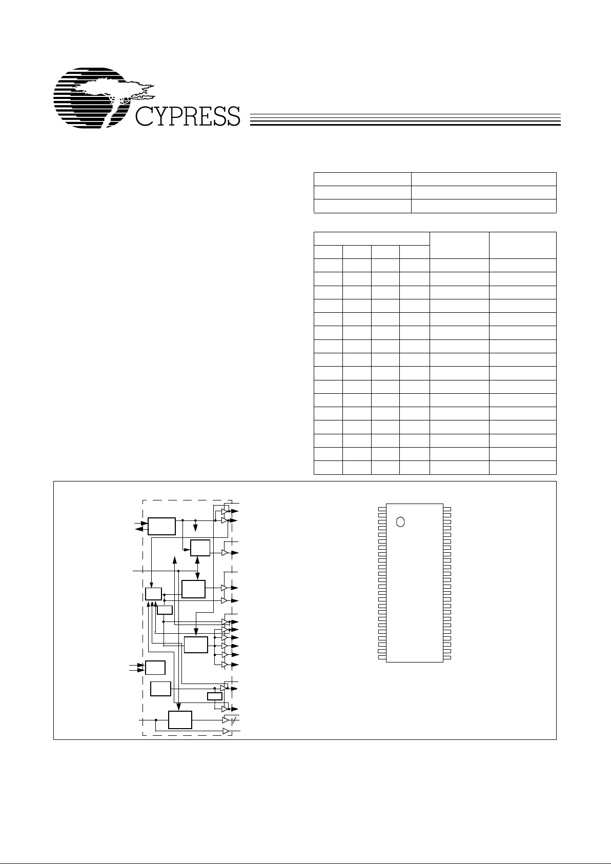
Logic Block Diagram
Pin Configuration
[1]
VDDQ3
REF0/(PCI_STOP#)
GND
X1
X2
VDDQ3
PCI_F/MODE
PCI1/FS3
GND
PCI2
PCI3
PCI4
PCI5
VDDQ3
SDRAMIN
GND
SDRAM11
SDRAM10
VDDQ3
SDRAM9
SDRAM8
GND
SDATA
SCLK
W199
VDDQ2
IOAPIC
REF1/FS2*
GND
CPU_F
CPU1
VDDQ2
CLK_STOP#
SDRAM_F
GND
SDRAM0
SDRAM1
VDDQ3
SDRAM2
SDRAM3
GND
SDRAM4
SDRAM5
VDDQ3
SDRAM6
SDRAM7
VDDQ3
48MHz/FS0*
24MHz/FS1*
48
47
46
45
44
43
42
41
40
39
38
37
36
35
34
33
32
31
30
29
28
27
26
25
1
2
3
4
5
6
7
8
9
10
11
12
13
14
15
16
17
18
19
20
21
22
23
24
I2C
{
VDDQ3
REF0/(PCI_STOP#)
VDDQ2
CPU1
PCI_F/MODE
XTAL
PLL Ref Freq
PLL 1
X2
X1
REF1/FS2
VDDQ3
Stop
Clock
Control
Stop
Clock
Control
PCI2
PCI3
PCI4
48MHz/FS0
24MHz/FS1
PLL2
÷2,3, 4
OSC
VDDQ2
CLK_STOP#
VDDQ3
IOAPIC
PCI5
I2C
SDATA
Logic
SCLK
I/O Pin
Control
SDRAM0:11
SDRAMIN
12
VDDQ3
PCI1/FS3
Stop
Clock
Control
Stop
Clock
Control
CPU_F
÷2
SDRAM_F
Page 2
W199
PRELIMINARY
2
Pin Definitions
Pin Name Pin No.
Pin
T ype Pin Description
CPU_F 44 O
Free-running CPU Clock :
Output voltage swing is controlled by the voltage applied to
VDDQ2. See Tables 2 and 6 for detaile d frequency information.
CPU1 43 O
CPU Clock Output 1:
This CPU clock output is controlled by the CLK_STOP# control
pin. Output voltage swing is controlled by voltage appli ed to VDDQ2.
PCI2:5 10, 11, 12, 13O
PCI Clock Outputs 2 through 5:
These four PCI clock outputs are controll ed by the
PCI_STOP# contr ol pin. Output vol tage swing is cont rolled by vol tage applied to VDDQ3.
PCI1/FS3 8 I/O
Fixed PCI Clock Outpu t:
As an output. f requency is set b y the FS0 :3 inp uts or t hrough
serial input interface, see Tables 2 and 6. This output is affected by the PCI_STOP#
input. When an input, latches data sel ecting the frequency of the CPU and PCI ou tputs.
PCI_F/MODE 7 I/O
Fixed PCI Clock Outpu t:
As an output, f requency is set b y the FS0 :3 inp uts or t hrough
serial input int erf a ce, se e Tables 2 and 6. Thi s outpu t is no t aff ect ed b y the PCI _ST OP#
input. When an input, sets function of pin 2.
CLK_STOP# 41 I
CLK_STOP# Input:
When brought LOW, af f ect ed cloc k output s are s top ped LOW aft er
completing a full clock cycle (2–3 CPU clock latency). When brought HIGH, affected
clock output s start, beginning with a full cloc k cycle (2–3 CPU clock lat ency).
IOAPIC 47 O
IOAPIC Cloc k Output:
Provides 14.318-MHz fi xed f requency. The output volta ge swing
is controlled by VDDQ2. This output is disabled when CLK_STOP# is set LOW.
48MHz/FS0 26 I/O
48-MHz Output:
48 MHz is provided in normal operation. In standard syst em s, this
output can be used as the reference for the Universal Serial Bus. Upon power-up FS0
input will be latched, which will set clock frequencies as described in Table 2.
24MHz/FS1 25 I/O
24-MHz Output:
24 MHz is provided in normal operation. In standard syst em s, this
output can be used as the cloc k input f or a Super I/O chip. Up on power -up FS1 input will
be latched, which will set clock frequencies as described in Table 2.
REF1/FS2 46 I/O
I/O Dual-Functio n REF0 a nd FS2 pin:
Upon power-up , FS2 input will be latched which
will set clock f requencies as described in Table 2. When an output, this pin provides a
fixed cl ock signal equal in frequency to the reference sig nal provided at the X1/X2 pins.
REF0/
(PCI_STOP#)
2I/O
Fixed 14.318-MHz Output 0 or PCI_STOP# Pin:
Function determined by MODE pin.
The PCI_STOP# input enables the PCI 1:5 outputs when HIGH and causes them to
remain at logic 0 when LO W. The PCI_STOP signal is latc hed on the rising edge of
PCI_F. Its effects take place on the next PCI_F clock cycle. When an output, this pin
provides a fixed clock signal equal in frequency to the reference signal provided at the
X1/X2 pins.
SDRAMIN 15 I
Buffered Input Pin:
The signal provided to this input pin is buffered to 13 outputs
(SDRAM0:11, SDRAM_F).
SDRAM0:11 38, 37, 35,
34, 32, 31,
29, 28, 21,
20, 18, 17
O
Buffered Outputs:
These twelve ded icate d outp uts pro vide copi es of th e signal provi ded at the SDRAMIN input. The swing is set by VDDQ3, and they ar e deactivated when
CLK_STOP# input is set LOW.
SDRAM_F 40 O
Free-running Buff ered Output:
This dedic ated output pro vides a cop y of the SDRAMIN
input which is not affected by the CLK_STOP# input
SCLK 24 I Clock pin for I
2
C circuitry.
SDATA 23 I/O Data pin for I
2
C circuitry.
X1 4 I
Crystal Connection or External Refe rence Frequen cy Input:
This pin has dual functions. It can be used as an external 14.318-MHz crystal connection or as an external
reference frequency input.
X2 5 I
Crystal Connection:
An input connection for an external 14.318-MHz crystal. If using
an external reference, this pin must be left unconnected.
VDDQ3 1, 6, 14, 19,
27, 30, 36
P
Power Connecti on:
Power supply for core logic, PLL circuitry, SDRAM outputs, PCI
outputs, r efe rence out puts , 48 -MHz ou tput, and 24 -MHz out put. Connect t o 3.3V supp ly
VDDQ2 42, 48 P
Power Connecti on:
Po wer supply for IOAPIC, CPU_F, and CPU1 output buffers. Con-
nect to 2.5V or 3.3V.
GND 3, 9, 16, 22,
33, 39, 45
G
Ground Connections:
Connect all ground pins to t he com m on system ground plane.
Page 3
W199
PRELIMINARY
3
Overview
The W199 was developed as a single-chip device to meet the
clocking needs of the VIA Apollo Pro-133 core logic chip set.
In addition to the typical outputs provided by standard
100-MHz FTGs, the W199 adds a thirteenth outpu t buffer , supporting SDRAM DIMM modules in conjunction with the
chipset.
Cypress’s proprietary spread spectrum frequency synthesis
technique is a feature of the CPU and PCI outputs. When enabled, th is featur e reduces the peak EMI measurement s of not
only the output signals and their harmonics, but also of any
other cloc k signals that are properly syn chronized to them.
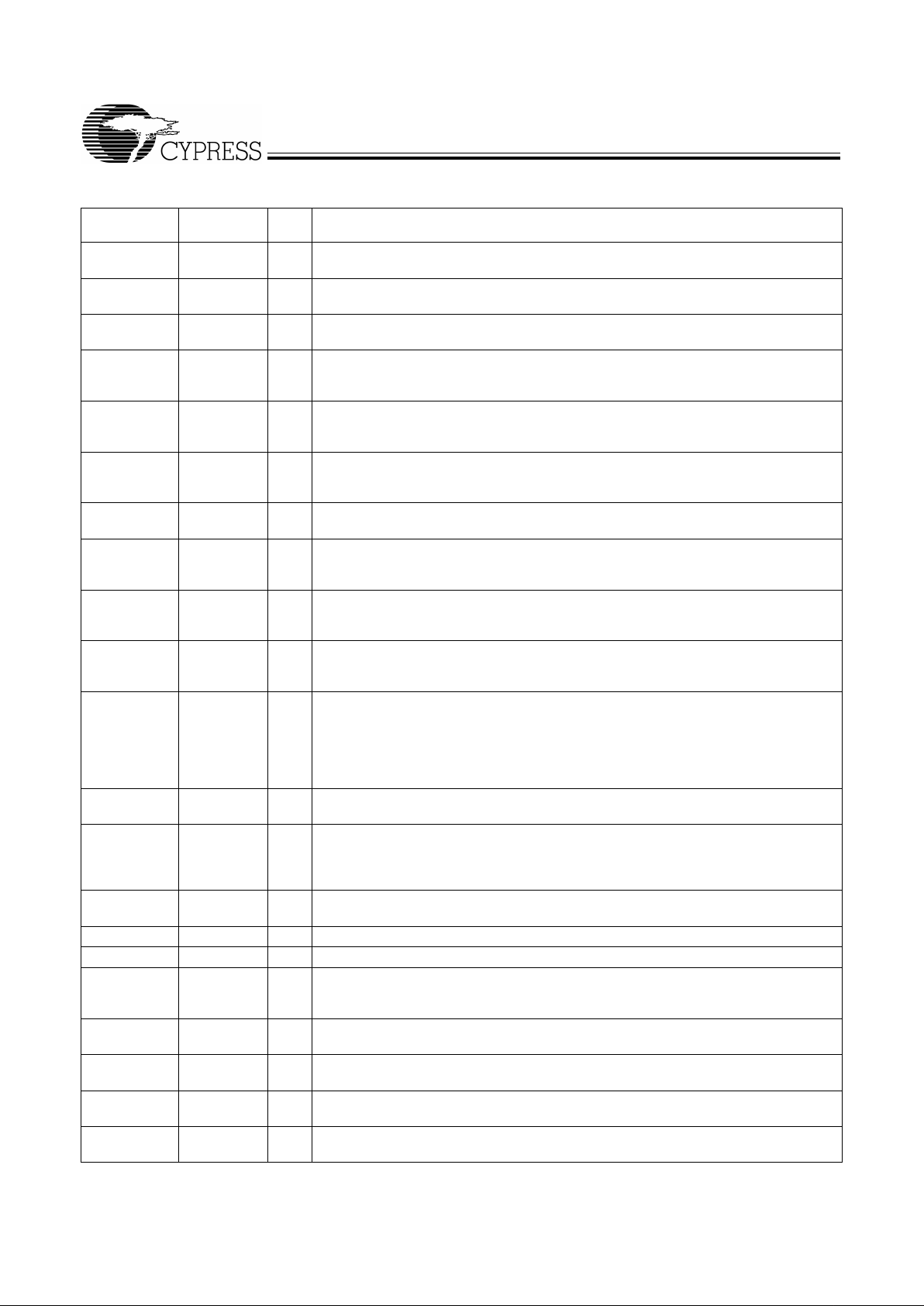
Functional Description
I/O Pin Operation
Pins 7, 8, 25 , 26, are 46 are dual-pu rpose l/O pins . Upon po wer-up these pins act as logic in puts, al lowing the dete rmination
of assigned device functions. A short time after power-up, the
logic state of each pin is latched and the pins become clock
outputs. This feature reduces device pin count by combining
clock outputs with input select pins.
An external 10-kΩ “strapping” resistor is connected between
the l/O pin and ground or V
DD
. Connection to ground sets a
latch to “0,” connection to V
DD
sets a latch to “1.” Fig ure 1 an d
Figure 2 show two suggested methods for strapping resistor
connections.
Upon W199 power-up, the first 2 ms of operation is used for
input logic selection. During th is period, the fiv e I/O pins (7, 8 ,
25, 26, 46) are three-stated, allowing the output strapping resistor on the l/O pins to pull the pins and their associated capacitiv e clock load to e ither a logic HIGH or LOW state . At the
end of the 2-ms period, the established logic “0” or “1” condition of the l/ O pin is latched. Next the output buffer is enabled,
converting the l/O pins into ope rating clock outputs. The 2-ms
timer starts when V
DD
reaches 2.0V. The input bits can only
be reset by turning V
DD
off and then back on again.
It should be noted that the strapping resistors have no significant effect on clock output signal integrity. The drive impedance of clock outputs is <40Ω (nominal), which is minimally
affected by the 10-kΩ strap to ground or V
DD
. As with the series termination resistor, the output strapping resistor should
be placed as close to the l/O pin as possible in order to keep
the interconnecting trace short. The trace from the resistor to
ground or V
DD
should be ke pt less t han tw o i nches i n lengt h to
minimize system noise coupling during input logic sampling.
When the clock outputs are enabled following the 2-ms input
period, the corresponding specified output frequency is delivered on the pin, assuming that V
DD
has stabilized. If VDD has
not yet reached full value, output frequency initially may be
below target but will increase to target once V
DD
voltage has
stabilized. In either case, a short output clock cycle may be
produced from the CPU clock outputs when the outputs are
enabled.
Power-on
Reset
Timer
Output Three -state
Data
Latch
Hold
QD
W199
V
DD
Clock Load
10 k
Ω
Output
Buffer
(Load Option 1)
10 k
Ω
(Load Option 0)
Output
Low
Output Strapping Resistor
Series Term ination R es istor
Figure 1. Input Logic Selection Through Resistor Load Option
Power-on
Reset
Timer
Output Three-state
Data
Latch
Hold
QD
W199
V
DD
Clock Load
R
10 k
Ω
Output
Buffer
Output
Low
Output Strapping Resistor
Series Termination Resistor
Jumper Opt i on s
Resistor Value R
Figure 2. Input Logic Selection Through Jumper Opti on
Page 4
W199
PRELIMINARY
4
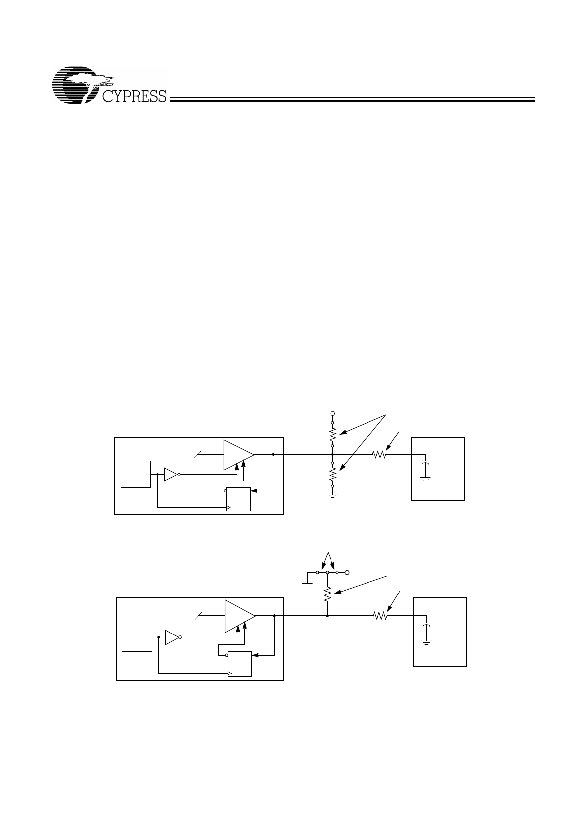
Spread Spectrum Frequency Tim ing G enera to r
The device generates a clock that is frequency modulated in
order to increase the bandwidth that it occu pies. By increas ing
the bandwidth of the fundamental and its harmonics, the amplitudes of the radiated electromagnetic emissions are reduced. This effect is depicted in Figure 3.
As shown in Figure 3, a harmonic of a modulated clock has a
much low er amplitude th an that of an un modulated si gnal. The
reduction in amplitude is dependent on the harmonic number
and the frequency deviation or spread. The equation for the
reduction is
dB = 6.5 + 9*log10(P) + 9*log10(F)
Where P is the perce nta ge of de viati on and F is the frequen cy
in MHz where the reduction is measured.
The output clock is modulated with a waveform depicted in
Figure 4. This waveform, as discussed in “Spread Spectrum
Clock Generation f or the Reducti on of Radiated Emissio ns” by
Bush, Fessler, and Hardin produces the maximum reduction
in the amplitude of radiated electromagnetic emissions. The
deviati on select ed for this chi p is speci fied in Table 7. Figure 4
details the Cypress spr eading pat tern. Cypress does offer options with more spread and greater EMI reduction. Contact
your local Sales representative for details on these devices .
Spread Spectrum clocking is activated or deactivated by selecting the appropriate v al ues fo r bits 1–0 in data byte 0 of the
I
2
C data stream. Refer to Table 7 for more d e ta ils.
Figure 3. Clock Harmonic with and without SSCG Modulation Freq uency Domain Representation
Spread
Spectrum
Enabled
EMI Reduction
Spread
Spectrum
Non-
MAX (0%)
MIN (–5%)
10%
20%
30%
40%
50%
60%
70%
80%
90%
100%
10%
20%
30%
40%
50%
60%
70%
80%
90%
100%
FREQUENCY
Figure 4. Typical Modulation Profile
Page 5
W199
PRELIMINARY
5
Serial Data Interface
The W199 features a two-pin, seri al data int erface that can be
used to configure internal register settings that control particular de vice funct ions. Upon power -up , the W199 i nitiali zes wit h
default register settings, therefore the use of this serial data
interface is optional. The serial interface is write-only (to the
clock chi p) and i s the dedi cated f unc tion of de v ice pi ns SDATA
and SCLOCK. In motherboard applications, SDATA and
SCLOCK are typically driven by two logic outputs of the
chipset. Clock device register changes are normally made
upon system initialization, if any are required. The interface
can also be used duri ng system operation for power management functions. Ta b le 3 summarizes the control functions of
the serial data interface.
Operation
Data is written to the W199 in elev en bytes of eight bits each .
Bytes are written in the order sho w n in Table 4.
T able 3. Serial Data Interface Control Func ti ons Sum mary
Control Function Description Common Application
Clock Output Disable Any individual clock output(s) can be disabled.
Disabled out puts are actively hel d LOW.
Unused outputs are disabled to reduce EMI
and system power. Examples are clock
outputs to unused PCI slots.
CPU Clock Frequency
Selection
Provides CPU/PCI fr equency selections through
software. Frequency is changed in a smooth and
controlled fashion.
For alternate microprocessors and power
management options. Smooth frequency
transition allows CPU frequency change
under normal system operation.
Spread Spectrum
Enabling
Enables or dis ables spread spectrum cl ocking. For EMI reduction.
Output Three-st ate Puts clock output into a high-impedance state. Production PCB testing.
(Reserved) Reserved function for future device revi sion or
production de vice testing.
No user application. Register bit must be
written as 0.
Table 4. Byte Writing Sequence
Byte
Sequence Byte Name Bit Sequence Byte Description
1 Slave Address 11010010 Commands the W199 to accept the bits in Dat a Bytes 0–6 for inte rn a l
register co nfigurati on. Since oth er devi ces may e xist on the same common serial dat a bus, it is n ecessary to ha ve a specific sl av e address for
each potential receiver. The slave receiver address for the W199 is
11010010. Regist er setting wi ll not be mad e if the Slav e Addr ess is not
correct (or is f or an alternate slave receiver) .
2 Command Code Don’t Care Unused by the W199, therefore bit values are ignored (“don’t care”).
This byte must be included in the data write sequence to maintain
proper by te allocation . The Command Code Byte is part of t he standard
serial communi ca tion protoc ol and ma y be use d whe n writi ng t o a nother addressed slave receiver on the serial data bus.
3 Byte Count Don’t Care Unused by the W199, therefor e bit values are ignored (“don’t care”).
This byte must be included in the data write sequence to maintain
proper byte allocation. The Byte Count Byte is part of the standar d
serial communi ca tion protoc ol and ma y be use d whe n writi ng t o a nother addressed slave receiver on the serial data bus.
4 Data Byte 0 Refer to Table 5 The data bit s in Data Bytes 0–7 s et internal W199 register s that c ontrol
device operation. The data bits are only accepted when the Address
Byte bit seq uence is 11010010, as noted above. For description of bit
control f unctions, refer to Table 5, Data Byte Serial Confi guration Map.
5 Data Byte 1
6 Data Byte 2
7 Data Byte 3
8 Data Byte 4
9 Data Byte 5
10 Data Byte 6
11 Data Byte 7
Page 6

W199
PRELIMINARY
6
Writing Data Bytes
Each bit in Data Bytes 0–7 control a particular device funct io n
except for the “reserved” bits which must be written as a lo gic
0. Bits are wri tten MSB (most signific ant bit) fi rst, which is bit 7.
Table 5 gives the bit f ormats f or regi sters loca ted in Dat a Bytes
0–7.
Ta ble 6 details additional frequency selections that are available through th e seria l dat a interface .
Table 7 details the select functions for Byte 0, bits 1 and 0.
Table 5. Data Bytes 0–7 Seri al Conf iguration Map
Bit(s)
Affected Pin
Control Function
Bit Control
DefaultPin No. Pin Name 0 1
Data Byte 0
7-- --(Reserved) -- -- 0
6 -- -- SEL_2 See Table 6 0
5 -- -- SEL_1 See Table 6 0
4 -- -- SEL_0 See Table 6 0
3 -- -- Hardware/Software F requency Select Hardware Software 0
2 -- -- SEL3 See Table 6 0
1–0-- -- Bit 1
Bit 0 Function (See Table 7 for function details)
0 0 Spread Spectrum Off (default)
0 1 (Reserved)
1 0 Spread Spectrum On
1 1 All Outputs Three-stated
00
Data Byte 1
7-- --(Reserved) -- -- 0
6-- --(Reserved) -- -- 0
5-- --(Reserved) -- -- 0
4-- --(Reserved) -- -- 0
3 40 SDRAM_F Clock Output Disable Low Active 1
2-- --(Reserved) -- -- 0
1 43 CPU1 C lock Outp u t D isable Low A ctive 1
0 44 CPU_F Clock Output Disable Low Active 1
Data Byte 2
7-- --(Reserved) -- -- 0
6 7 PC I_ F Clock O utput D isable Low A ctive 1
5-- --(Reserved) -- -- 0
4 13 P C I 5 Clock Outp u t D isable Low A ctive 1
3 12 P C I 4 Clock Outp u t D isable Low A ctive 1
2 11 P C I 3 Clock Outp u t D isable Low A ctive 1
1 10 P C I 2 Clock Outp u t D isable Low A ctive 1
0 8 PCI1 Clock Outp u t Disabl e Low Act ive 1
Data Byte 3
7-- --(Reserved) -- -- 0
6-- --(Reserved) -- -- 0
5 26 48MHz Clock Output Disable Low Active 1
4 25 24MHz Clock Output Disable Low Active 1
3-- --(Reserved) -- -- 0
Page 7

W199
PRELIMINARY
7
2 21, 20,
18, 17
SDR AM8:1 1 Clock Outpu t D isable Low A ctive 1
1 32, 31,
29, 28
SDRAM4:7 Clock Output Disable Low Active 1
0 38, 37,
35, 34
SDRAM0:3 Clock Output Disable Low Active 1
Data Byte 4
7-- --(Reserved) -- -- 0
6-- --(Reserved) -- -- 0
5-- --(Reserved) -- -- 0
4-- --(Reserved) -- -- 0
3-- --(Reserved) -- -- 0
2-- --(Reserved) -- -- 0
1-- --(Reserved) -- -- 0
0-- --(Reserved) -- -- 0
Data Byte 5
7-- --(Reserved) -- -- 0
6-- --(Reserved) -- -- 0
5-- --(Reserved) -- -- 0
4 47 IOAPIC Clock Output Disable Low Active 1
3-- --(Reserved) -- -- 0
2-- --(Reserved) -- -- 0
1 46 REF1 Clock Output D isable Low A ctive 1
0 2 REF0 Clock Output Disable Low Active 1
Data Byte 6
7-- --(Reserved) -- -- 0
6-- --(Reserved) -- -- 0
5-- --(Reserved) -- -- 0
4-- --(Reserved) -- -- 0
3-- --(Reserved) -- -- 0
2-- --(Reserved) -- -- 0
1-- --(Reserved) -- -- 0
0-- --(Reserved) -- -- 0
Data Byte 7
7-- --(Reserved) -- -- 0
6-- --(Reserved) -- -- 0
5-- --(Reserved) -- -- 0
4-- --(Reserved) -- -- 0
3-- --(Reserved) -- -- 0
2-- --(Reserved) -- -- 0
1-- --(Reserved) -- -- 0
0-- --
(Reserved) -- -- 0
Table 5. Data Bytes 0–7 Seri al Conf iguration Map
(continued)
Bit(s)
Affected Pin
Control Function
Bit Control
DefaultPin No. Pin Name 0 1
Page 8

W199
PRELIMINARY
8
Note:
2. CPU and PCI frequency selections are listed in
Table 2
and
Table 6
.
T able 6. Additional Frequency Selections through Serial Data Interface Data Bytes
Input Conditions Output Frequency
Data Byte 0, Bit 3 = 1
CPU, SDRAM
Clocks (MHz)
PCI Clocks
(MHz)
Bit 2
SEL_3
Bit 6
SEL_2
Bit 5
SEL_1
Bit 4
SEL_0
1 1 1 1 133.3 33.3 (CPU/4)
1 1 1 0 124 31 (CPU/4)
1 1 0 1 150 37.5 (CPU/4)
1 1 0 0 140 35 (CPU/4)
1 0 1 1 105 35 (CPU/3)
1 0 1 0 110 36.7 (CPU/3)
1 0 0 1 115 39.3 (CPU/3)
1 0 0 0 120 40 (CPU/3)
0 1 1 1 100 33.3 (CPU/3)
0 1 1 0 133 44.3 (CPU/3)
0 1 0 1 112 37.3 (CPU/3)
0 1 0 0 103 34.3 (CPU/3)
0 0 1 1 66.8 33.4 (CPU/2)
0 0 1 0 83.3 41.7 (CPU/2)
0 0 0 1 75 37.5 (CPU/2)
0 0 0 0 124 41.3 (CPU/3)
T able 7. Select Function for Data Byte 0, Bits 0:1
Function
Input Conditions Output Conditions
Data Byte 0
CPU_F,
CPU1
PCI_F,
PCI1:5
REF0:1,
IOAPIC 48MHZ 24MHZBit 1 Bit 0
Spread Spectrum On 1 0 –0.5% –0.5% 14.318 MHz 48 MHz 24 MHz
Spread Spectrum Off
(default)
0 0 Note 2 Note 2 14.318 MHz 48 MHz 24 MHz
Three-state 1 1 Hi-Z Hi-Z Hi-Z Hi-Z Hi-Z
Page 9

W199
PRELIMINARY
9
Absolute Maximum Ratings
Stresses gre ater th an those list ed i n this tab le may cause permanent damage to the de vice. These represent a str ess ratin g
only. Operation of the device at these or any other conditions
above those specified in the operating sect ions of this spec if ication is not implied. Maximum conditions for extended periods may affect reliability.
.
Parameter Description Rating Unit
V
DD
, V
IN
V oltage on any pin with respect to GND –0.5 to +7 .0 V
T
STG
Storage Temperature –65 to +150 °C
T
B
Ambient Temperature under Bias –55 to +125 °C
T
A
Operating Temperature 0 to +70 °C
ESD
PROT
Input ESD Protection 2 (min) kV
DC Electr i cal C h ar acteristics:
T
A
= 0°C to +70°C; V
DDQ3
= 3.3V±5%; V
DDQ2
= 2.5V±5%
Parameter Description Tes t Condi tion Min. Typ. Max. Unit
Supply Current
I
DD
3.3V Supply Current CPU_F: CPU1 = 100 MHz
Outputs Loaded
[3]
260 mA
I
DD
2.5V Supply Current CPU_F: CPU1 = 100 MHz
Outputs Loaded
[3]
25 mA
Logic Inputs
V
IL
Input Low Voltage GND – 0.3 0.8 V
V
IH
Input High Voltage 2.0 V
DDQ3
+
0.3
V
I
IL
Input Low Current
[4]
–25 µA
I
IH
Input High Current
[4]
10 µA
Clock Outputs
V
OL
Output Low Voltage IOL = 1 mA 50 mV
V
OH
Output High Voltage IOH = 1 mA 3.1 V
V
OH
Output High Voltage CPU_F:1, IOAPIC IOH = –1 mA 2.2 V
I
OL
Output Low Current CPU_F, CPU1 VOL = 1.25V 27 57 97 mA
PCI_F, PCI1:5 V
OL
= 1.5V 20.5 53 139 mA
IOAPIC V
OL
= 1.25V 40 85 140 mA
REF0:1 V
OL
= 1.5V 25 37 76 mA
48-MHz V
OL
= 1.5V 25 37 76 mA
24-MHz V
OL
= 1.5V 25 37 76 mA
I
OH
Output High Current CPU_F, CPU1 VOH = 1.25V 25 55 97 mA
PCI_F, PCI1:5 V
OH
= 1.5V 31 55 139 mA
IOAPIC V
OH
= 1.25V 40 87 155 mA
REF0:1 V
OH
= 1.5V 27 44 94 mA
48-MHz V
OH
= 1.5V 27 44 94 mA
24-MHz V
OH
= 1.5V 25 37 76 mA
Notes:
3. All clock outputs loaded with 6" 60Ω traces with 22-pF capacitors.
4. W199 logic inputs (except FS3) have internal pull-up devices (pull-ups not full CMOS level). Logic input FS3 has an internal pull-down device.
Page 10

W199
PRELIMINARY
10
AC Electrical Characteristics
TA = 0°C to +70°C; V
DDQ3
= 3.3V±5%; V
DDQ2
= 2.5V±5%; f
XTL
= 14.31818 MHz
AC clock parameters are tested and guaranteed over stated operating conditions using the stated lump capacitive load at the
clock output; Spread Spec trum clocking is disabled.
Crystal Oscillator
V
TH
X1 Input threshold Voltage
[5]
V
DDQ3
= 3.3V 1.65 V
C
LOAD
Load Capacitance, Imposed on
External Crystal
[6]
14 pF
C
IN,X1
X1 Input Capacitance
[7]
Pin X2 unconnected 28 pF
Pin Capacitance/Induct ance
C
IN
Input Pin Capacitance Except X1 and X2 5 pF
C
OUT
Output Pin Capacitance 6pF
L
IN
Input Pin Inductance 7nH
Notes:
5. X1 input threshold voltage (typical) is V
DDQ3
/2.
6. The W199 contains an internal crystal load capacitor between pin X1 and ground and another between pin X2 and ground. Total load placed on crystal is
14 pF; this includes typical stray capacitance of short PCB traces to crystal.
7. X1 input capacitance is applicable when driving X1 with an external clock source (X2 is left unconnected).
DC Electr i cal C h ar acteristics:
(continued) T
A
= 0°C to +70°C; V
DDQ3
= 3.3V±5%; V
DDQ2
= 2.5V±5%
Parameter Description Tes t Condi tion Min. Typ. Max. Unit
CPU Clock Outputs, CPU_F, CPU1 (Lump Capacitance Test Load = 20 pF)
Parameter Description Test Condition/Comments
CPU = 66.8 MHz CPU = 100 MHz CPU = 133 MHz
UnitMin. Typ. Max. Min. Typ. Max. Min. Typ. Max.
t
P
Pe riod Measured on rising edge at
1.25
15 15.5 10 10.5 7.5 8.0 ns
t
H
High Time Duration of clock cycle above
2.0V
5.2 3.0 1.87 ns
t
L
Low Time Duration of clock cycle below
0.4V
5.0 2.8 1.67 ns
t
R
Output Rise
Edge Rate
Measured from 0.4V to 2.0V 1 4 1 4 1 4 V/ns
t
F
Output F all Edge
Rate
Measured from 2.0V to 0.4V 1 4 1 4 1 4 V/ns
t
D
Duty Cycle Measured on rising and falling
edge at 1.25V
45 55 45 55 45 55 %
t
JC
Jitter,
Cycle-to-Cycle
Measured on rising edge at
1.25V. Maximum difference of
cycle time between two
adjacent cycles .
200 200 200 ps
t
SK
Output Skew Measured on rising edge at
1.25V
175 175 175 ps
f
ST
Frequency Stabilization from
Po wer-up (cold
start)
Assumes full supply voltage
reached within 1 ms from power-up. Short cycles e xist prior to
frequency stabi li zation.
333ms
Z
o
AC Output
Impedance
Ave rage v alue d urin g swi tchi ng
transition. Used f or determini ng
series termination value.
20 20 20 Ω
Page 11

W199
PRELIMINARY
11
PCI Clock Outputs, PCI_F and PCI1:5 (L ump Capacit ance Test Load = 30 pF)
Parameter Description Test Condition/Comments Min. Typ. Max. Unit
t
P
Period Measured on rising edge at 1.5V 30 ns
t
H
High Time Duration of clock cycle above 2.4V 12.0 ns
t
L
Low Time Duration of clock cycle below 0.4V 12.0 ns
t
R
Output Rise Edge Rate Measured fr om 0.4V to 2.4V 1 4 V/ns
t
F
Output Fall Edge Rate Measured from 2.4V to 0.4V 1 4 V/ns
t
D
Duty Cycle Measure d on rising an d falli ng edge at 1.5 V 45 55 %
t
JC
Jitter , Cycle-to-Cycle Meas ured on rising edge at 1.5V. Maximum
diffe rence of cycle time between two adjacent cycles.
250 ps
t
SK
Output Skew Measured on rising edge at 1.5V 500 ps
t
O
CPU to PCI Clock Skew Covers all CPU/PCI outputs. Measured on
rising edge at 1.5V. CPU leads PCI output.
1.5 4 ns
f
ST
Frequency Stabilization
from Po we r-up ( cold s tart)
Assumes full supp ly voltage reach ed within
1 ms from power -up. Short cycles exist prior to frequency stabi lization.
3ms
Z
o
AC Output Impedance Average value during switching transition.
Used for determining series termination
value.
30 Ω
IOAPIC Clock Output (Lump Capacitance Test Load = 20 pF)
Parameter Description Tes t Condi ti on/Comments
CPU = 66.6/100 MHz
UnitMin. Typ. Max.
f Frequency, Actual Frequency gene rated by crystal oscillator 14.31818 MHz
t
R
Output Rise Edge Rate Measured from 0.4V to 2.0V 1 4 V/ ns
t
F
Output Fall Edge Rate Measured from 2.0V to 0.4V 1 4 V/ns
t
D
Duty Cycle Measured on rising and falling edge at 1.25V 45 55 %
f
ST
Frequency Stabilization
from P ower-up (cold st art)
Assumes full supply voltage reached within
1 ms from power-up. Short cycles exist pri or
to frequency stabilization.
1.5 ms
Z
o
AC Output Impedance Average value during switching transition.
Used for determining seri es termination value .
15 Ω
SDRAM Clock Outputs, SDRAM, SDRAM0:11 (Lump Capacitance Test Load = 30 pF)
(continued)
Page 12

W199
PRELIMINARY
12
SDRAM 0:11,_F Clock Outputs (Lump Capacitance Test Load = 22 pF)
Parameter Descri pti on Test Condition/Comments
SDRAMIN =
66.8 MHz
SDRAMIN =
100 MHz
SDRAMIN =
133 MHz
UnitMin. Typ. Max. Min. Typ. Max. Min. Typ. Max.
t
P
Period Measured on rising edge at
1.5V
15 15.5 10 10.5 7.5 8.0 ns
t
H
High Time Duration of cl ock cycle above
2.4V
5.2 3.0 1.87 ns
t
L
Low Time Duration of clock cycle below
0.4V
5.0 2.0 1.67 ns
t
R
Output Rise Edge
Rate
Measured from 0.4V to 2.4V 1 4 1 4 1 4 V/ns
t
F
Output Fall Edge
Rate
Measured from 2.4V to 0.4V 1 4 1 4 1 4 V/ns
t
D
Duty Cycle Measured on rising and f al ling
edge at 1.5V
45 55 45 55 45 55 %
t
JC
Jitter,
Cycle-to-Cycle
Measured on rising edge at
1.5V. Maximum difference of
cycle time between two adjacent cycles.
250 250 250 ps
t
SK
Output Skew Measured on rising and falling
edge at 1.5V
250 250 250 ps
t
PD
Propagation
Delay
Measured from SDRAMIN 3.7 3.7 3.7 ns
Z
o
AC output
Impedance
Av erage value during swit ching
transition. Used for determining series termination value.
15 15 15 Ω
REF0:1 Clock Outputs (Lump Capacitance Test Load = 20 pF)
Parameter Description Test Condition/Comments Min. Typ. Max. Unit
f Frequency, Actual Frequency generated by crystal oscillator 14.318 MHz
t
R
Output Rise Edge Rate Measured from 0.4V to 2.4V 0.5 2 V/ns
t
F
Output Fall Edge Rate Measured from 2.4V to 0.4V 0.5 2 V/ns
t
D
Duty Cycle Measured on rising and falling edge at 1.5V. 45 55 %
f
ST
Frequency St abiliza tion
from Power-up (cold
start)
Assumes full suppl y vo ltage r each ed withi n 1 ms from
power-up. Short cycles exist prior to frequency stabilization.
3ms
Z
o
AC Output Impedance Av er age v al ue durin g s wit ching tran si tion. Used for de-
termining series termination v a lue.
40 Ω
Page 13

W199
PRELIMINARY
13
Document #: 38-00858
48-MHz Clock Output (Lump Capacit ance Test Load = 20 pF)
Parameter Description Tes t Condi tion/Comments Min. Typ. Max. Unit
f Frequency, Actual Determined by PLL divider ratio (see m/n below) 48.008 MHz
f
D
Deviatio n fro m 48 MHz (48.008 – 48)/48 +167 ppm
m/n PLL Ratio (14.31818 MHz x 57/ 17 = 48.008 MHz) 57/17
t
R
Output Rise Edge Rate Measured from 0.4V to 2.4V 0.5 2 V/ns
t
F
Output Fall Edge Rate Measured from 2.4V to 0.4V 0.5 2 V/ns
t
D
Duty Cycle Measured on rising and falling edge at 1.5V 45 55 %
f
ST
Frequency Stabiliza ti on
from Power-up (cold
start)
Assumes full supply voltage reached within 1 ms from
power-up. Short cycles exist prior to frequency
stabilization.
3ms
Z
o
AC Output Imped ance Averag e value during swit ching transition. Used for de-
termining series terminati on value.
40 Ω
24-MHz Clock Output (Lump Capacit ance Test Load = 20 pF)
Parameter Description Test Condition/Comments Min. Typ. Max. Unit
f Frequency, Actual Determined by PLL divider ratio (s ee m/n below) 24.004 MHz
f
D
Deviati on from 24 MHz (24.004 – 24) /24 +167 ppm
m/n PLL Ratio (14.31818 MHz x 57/34 = 24.004 MHz) 57/34
t
R
Output Rise Edge Rate M easured from 0.4V to 2.4V 0.5 2 V/ns
t
F
Output Fall Edge Rate Measured from 2.4V to 0.4V 0.5 2 V/ns
t
D
Duty Cycle Measured on rising and falling edge at 1.5V 45 55 %
f
ST
Frequency Stabiliza-
tion from P ower-up
(cold start)
Assumes full supply v ol tage reac hed withi n 1 ms from
power-up. Short cycles exist prior to frequency stabilization.
3ms
Z
o
AC Output Impedance Av er ag e val ue du ring s witch ing tr ansit ion. Used f or de-
termining series termination value.
40 Ω
Ordering Information
Ordering Code
Package
Name Package Type
W199 H 48-Pin SSOP (300-mil)
Page 14

W199
PRELIMINARY
© Cypress Semiconductor Corporation, 1999. The information contained herein is subject to change without notice. Cypress Semiconductor Corporation assumes no responsibility for the use
of any circuitry other than circuitry embodied in a Cypress Semiconductor product. Nor does it con vey or imply any license under patent or other rights. Cypress Semiconductor does not authorize
its products for use as critical components in life-support systems where a malfunction or failure may reasonably be expected to result in significant injury to the user. The inclusion of Cypress
Semiconductor products in life-support systems application implies that the manufacturer assumes all risk of such use and in doing so indemnifies Cypress Semiconductor against all charges.
Package Diagram
48-Pin Shrink Small Outline Package (SSOP, 300 mils)
Summary of nominal dimensions in inches:
Body Width: 0.296
Lead Pitch: 0.025
Body Length: 0.625
Body Height: 0.102
 Loading...