

Page 1
Spread Spectrum FTG for 440BX and VIA Apollo Pro-133
W196
PRELIMINARY
Cypress Semiconductor Corporation
• 3901 North First Street • San Jose • CA 95134 • 408-943-2600
October 28, 1999, rev. **
Features
• Maximized EMI suppression usi ng Cypress’s Spread
Spectrum Technology
• System frequency synthesizer for 440BX, 440ZX, and
VIA Apollo Pro-133
•I
2
C programmabl e to 155 MHz (32 sel ectable
frequencies)
• T wo skew-controll ed copies of CPU output
• Seven copies of PCI output (synchronous w/CPU output)
• One copy of 14.31818-MHz IOAPIC output
• One copy of 48-MHz USB output
• Selectable 24-/48-MHz clock is determined by resistor
straps on power up
• One high-drive outpu t buffer that pr oduces a copy of
the 14.318-MHz reference
• Isolated core VDD pin for noise reduction
Key Specific ati o n s
Supply Voltages:.......................................V
DDQ3
= 3.3V±5%
V
DDQ2
= 2.5V±5%
CPU Cy cl e to Cyc le Jitter: ..........................................250 ps
CPU, PCI Output Edge Rate:
.........................................≥
1 V/ns
CPU0: 1 O u tp u t Skew : .. ... .. .........................................17 5 p s
PCI_ F, PCI1:6 Out p u t Skew: ...... .. .. .............................50 0 p s
CPU to PCI Skew: ........................ 1.5 to 4.0 ns (CPU Leads)
REF2X/SEL48#, SCLOCK, SDATA:...............250-kΩ pull-up
FS1:............................................................250-kΩ pull- d own
FS0:...................................................No pull-up or pull-down
Note:
Internal pull-up or pull-down resistors should not be re-
lied upon for setting I/O pins HIGH or LOW.
T able 1. Pin Selectable Frequency
FS1 FS0 CPU(0:1) PCI
1 1 133.3 MHz 33.3 MHz
1 0 105 MHz 35 MHz
0 1 100 MHz 33.3 MHz
0 0 66.8 MHz 33.3 MHz
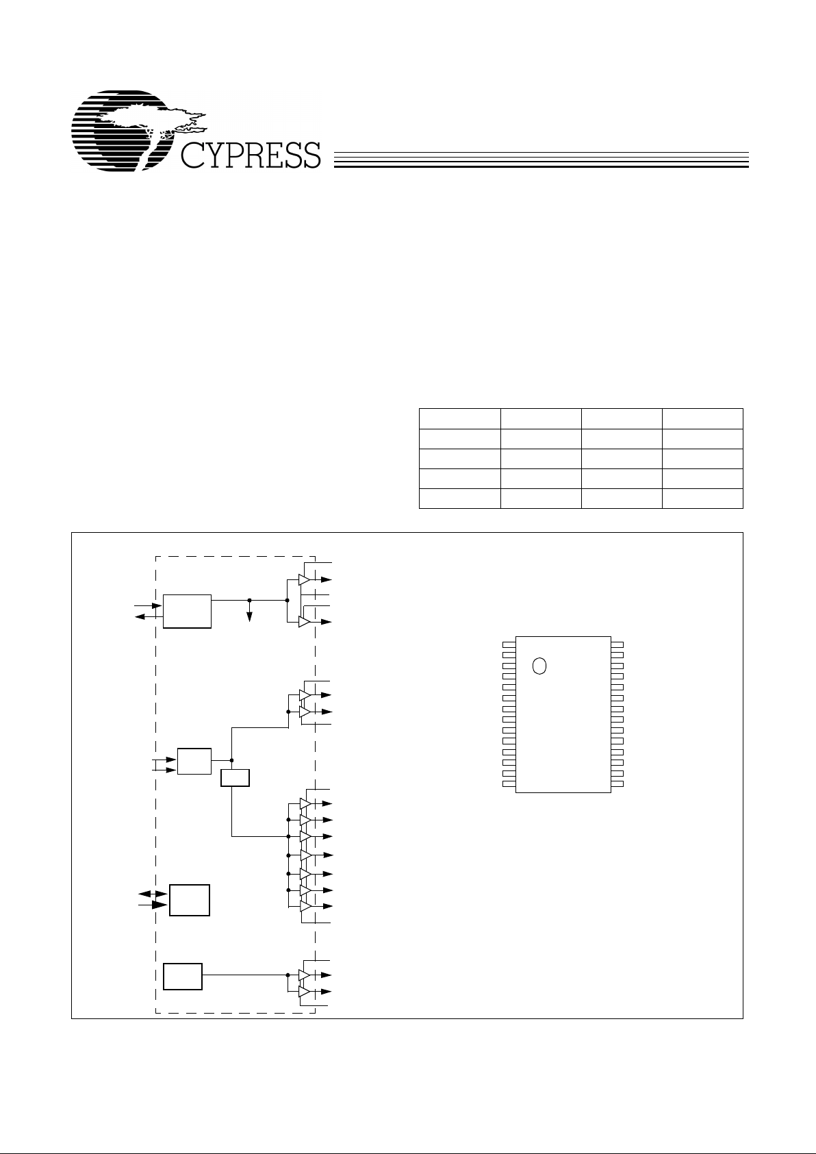
Pin ConfigurationBlock Diagram
X1
X2
GND
PCI_F
PCI1
PCI2
PCI3
PCI4
VDDQ3
PCI5
PCI6
VDDQ3
48MHz
24_48MHz/FS1
GND
REF2X/SEL48#
VDDQ3
VDDQ2
IOAPIC
VDDQ2
CPU0
CPU1
VDDQ3
GND
SDATA
SCLOCK
FS0
GND
28
27
26
25
24
23
22
21
20
19
18
17
16
15
1
2
3
4
5
6
7
8
9
10
11
12
13
14
VDDQ3
REF2X/SEL48#
VDDQ3
IOAPIC
CPU0
CPU1
PCI_F
XTAL
PLL Ref Fre q
PLL 1
FS1
X2
X1
VDDQ3
PCI1
PCI2
PCI3
PCI4
PCI5
48MHz
24_48MHz/FS1
PLL2
÷2/÷3
OSC
VDDQ2
PCI6
GND
GND
VDDQ3
GND
GND
I2C
SCLOCK
SDATA
LOGIC
FS0
Page 2
W196
PRELIMINARY
2
Pin Definitions
Pin Name
Pin
No.
Pin
Type Pin Description
CPU0:1 22, 21 O
CPU Clock Output s 0 thr ough 1:
These two CPU clo c ks run at a freque ncy s et by
FS0:1 or the serial dat a interface. See Table 1 and Table 5. Output voltage swing is
set by the v olt age applied to VDDQ2.
PCI1:6
PCI_F
5, 6, 7, 8, 10,
11, 4
O
PCI Bus Clock Outputs 1 thro ugh 6 and PCI_F:
These sev en PCI cl ock outputs
run synchronousl y to t he CPU clock. Voltage swing is set by the power connection
to VDDQ3.
IOAPIC 24 O
I/O APIC Clock Output:
Provides 14. 318-MHz fi xed fr equ ency. The output voltage
swing is set by the power connec ti on to VDDQ2.
48MHz 13 O
48-MHz O u tput:
Fixed 48-MHz USB clock. Output voltage swing is controlled by
voltage applied to VDDQ3.
24_48MHz/FS1 14 I/O
24-MHz or 48-MHz Output/Frequenc y Select 1 Input:
Frequenc y is set by the state
of pin 27 on power-up. This pin doubles as the select strap to determine device
operating frequency as described in Table 1.
REF2X/SEL48# 27 I/O
I/O Dual-Function REF2X and SEL48# Pin:
Upon power-up, the state of SEL48#
is latched. The initial state is set by either a 10K resistor to GND or to V
DD
. A 10K
resistor to GND causes pin 14 to output 48 MHz. If the pin is strapped to V
DD
, pin
14 will output 2 4MHz. Afte r 2 ms, the pin becomes a high-dri ve out put that produces
a copy of 14.318 MHz.
FS0 16 I
Frequency Selection 0 Input:
Selects CPU cloc k fr equency as shown in Table 1
on page 1.
SDATA 18 I/O
I
2
C Data Pin:
Data should be presented to thi s input as described in the I
2
C section
of this data sheet. Internal 250-kΩ pull-up resistor.
SCLOCK 17 I
I
2
C Clock Pin:
The I
2
C Data cloc k shoul d be p resente d to this input as describ ed in
the I
2
C section of this data shee t.
X1 1 I
Crystal Connection or External Reference Frequency Input:
Connec t to eit h er
a 14.318-MHz crystal or other reference signal.
X2 2 I
Crystal Connection:
An input connection for an ext ernal 14. 318-MHz crystal. If
using an external referen ce, this pin must be lef t unconnected.
VDDQ3 9, 12, 20, 26 P
Po wer Connectio n:
Pow er suppl y for core logic and PLL circ uitry, PCI, 48/24MHz,
and Reference output buffers. Connect to 3.3V supply.
VDDQ2 23, 25 P
Po we r Connection:
Power supply for IOAPIC and CPU output buffers. Connect to
2.5V supply.
GND 3, 15, 19, 28 G
Ground Connection s:
Connect all ground pins to the common system ground
plane.
Page 3
W196
PRELIMINARY
3
Functional Description
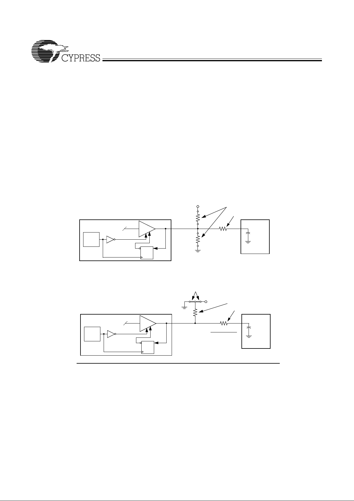
I/O Pin Operation
Pins 14 and 27 are dual-purpose l/O pins. Upon power-up
these pins act as logic inputs, allowing the determination of
assigned device functions. A short time after power-up, the
logic state of these pins is latched and the pi ns become clock
outputs. This feature reduces device pin count by combining
clock outputs with input select pins.
An external 10-kΩ “strapping” resistor is connected between
the l/O pin and ground or V
DD
. Connection to ground sets a
latch to “0”, connection to V
DD
sets a latch to “1.” Fig ure 1 an d
Figure 2 show two suggested methods for strapping resistor
connections.
Upon W196 power-up, the first 2 ms of operation is used for
input logic selection. During this period, the REF2X and
24_48MHz clock output buffers are three-stated, allowing the
output strapping resistor on the l/O pin to pull the pin and its
associated c apacitiv e cloc k load to either a l ogic HIGH or LOW
state. At the end of the 2-ms period, the established logic “0”
or “1” condition of the l/O pin is then latched. Next the output
buffer is enabled, which converts the l/O pin into an operating
clock output. The 2-ms timer is started when V
DD
reaches
2.0V. The input bits can only be reset by turning V
DD
off and
then back on again.
It should be noted that the strapping resistors have no signifi-
cant effect on clock output signal integrity. The drive impedance of the clock output is 20Ω (nominal), which is minimally
affected by the 10-kΩ strap to ground or V
DD
. As with the series termination resistor, the output strapping resistor should
be placed as close to the l/O pin as possible in order to keep
the interconnecting trace short. The trace from the resistor to
ground or V
DD
should be ke pt less t han tw o i nches i n lengt h to
prevent system noise coupling during input logic sam pling.
When the clock output is en abled following the 2-ms input pe-
riod, a 14.318-MHz output frequency is delivered on the pin,
assuming that V
DD
has stabilized. If VDD has not yet reached
full value , output frequency initi ally ma y be belo w target b ut will
increase to target once V
DD
voltage has stabilized. In either
case, a short output clock cycle may be produced from the
CPU clock outputs when the outputs are enabled.
Power-on
Reset
Timer
Output Three-state
Data
Latch
Hold
QD
W196
V
DD
Clock Load
10 k
Ω
Output
Buffer
(Load Option 1)
10 k
Ω
(Load Option 0)
Output
Low
Output Strapping Resistor
Series Termination Res istor
Figure 1. Input Logic Selection Through Resistor Load Option
Power-on
Reset
Timer
Output Three-state
Data
Latch
Hold
QD
W196
V
DD
Clock Load
R
10 k
Ω
Output
Buffer
Output
Low
Output Strapping Resistor
Series Termination Resistor
Jumper Options
Resistor Value R
Figure 2. Input Logic Selection Through Jumper Option
Page 4
W196
PRELIMINARY
4
Serial Data Interface
The W196 features a two-pi n, serial data interface that can be
used to configure internal register settings that control particular de vice funct ions. Upon power -up , the W196 i nitiali zes wit h
default register settings. Therefore, the use of this serial data
interface is optional. The serial interface is write-only (to the
clock chi p) and i s the dedi cated f unc tion of de v ice pi ns SDAT A
and SCLOCK. In motherboard applications, SDATA and
SCLOCK are typically driven by two logic outputs of the
chipset. Clock device register changes are normally made
upon system initialization, if required. The interface can also
be used during system ope ration f or pow er management functions. Table 2 summarizes the control functions of the serial
data interface.
Operation
Data is written to the W196 in ten bytes of eight bits each.
Bytes are written in the order sho w n in Table 3.
T able 2. Serial Data Interface Contr ol Functions Summary
Control Function Description Common Application
Clock Output Disable Any individual clock output(s) can be disabled.
Disabled out puts are actively held LOW.
Unused outputs are disabled to reduc e EMI and
system power. Examples are clock outputs to unused PCI slots.
CPU Clock Fr eque ncy
Selection
Provides CPU/PCI frequency selections beyond
the selections t hat are provi ded by the FS0:1 pins .
Frequenc y is changed in a smooth and contr olled
fashion.
For alternate microprocessor s and power management options. Smooth frequency tr ansition allows CPU fr equency change unde r normal system
operation.
Output Three-state Puts all c lock ou tputs into a h igh-impedan ce state . Production PCB testing.
Test Mode All clock outputs toggle in relation to X1 input, in-
ternal PLL is bypassed. Refer to Table 4.
Production PCB testi ng.
(Reserved) Reserved funct ion for future de vice revis ion or pro-
duction device testing.
No user application. Register bit must be writte n
as 0.
Table 3. Byte Writing Sequence
Byte
Sequence Byte Name Bit Sequenc e Byte Description
1 Slave Address 11010010 Commands the W196 to accept the bits in Data Byte s 3 –6 f or internal
register configuration. Since other devic es may exist on the same common serial data bus , i t is necessary to have a specific slave address f or
each potential receiver. The slave receiv er address for the W196 is
11010010. Register setting will not be made if the Slave Address is not
correct (or is for an alternate slave receiver).
2 Command
Code
Don’t Care Unused by the W196, theref ore bit v alues are ignor ed (“don’t care”). This
byte must be inc luded in the data write seq uence to main tain proper by te
allocation. The Command Code Byte is part of the standard serial communication pr otocol and may be used when writ ing to another addressed
slave receiver on the seri al dat a bus.
3 Byte Count Don’t Care Unused by the W196, t herefor e bit value s are ignored ( “don’t care”). This
byte must be inc luded in the data write seq uence to main tain proper by te
allocation. The Byt e Count Byte is part of the standard serial communication proto col and may b e used when writi ng to another addre ssed sla ve
receiver on the serial data bus.
4 Data Byte 0 Don’t Care Refer to Cypress SDRAM drivers.
5 Data Byte 1
6 Data Byte 2
7 Data Byte 3 Refer to Table 4 The data bits in these byt es set internal W196 registers that cont rol device
operation. The data bits are only accepted when the Address Byte bit
sequence is 11010010, as noted above. For description of bit control
functions, refer to Table 4, Data Byte Serial Configuration Map.
8 Data Byte 4
9 Data Byte 5
10 Data Byte 6
Page 5

W196
PRELIMINARY
5
Writing Data Bytes
Each bit in the data bytes control a particular device function
except for the “reserved” bits which must be written as a logic
0. Bits are written MSB (most significant bit) first, which is bit
7. Table 4 gives the bit formats for registers located in Data
Bytes 3–6.
Ta ble 5 details additional frequency selections that are available through th e seria l dat a interface.
Table 6 details the select functions for Byt e 3, bits 1 and 0.
Note:
1. Bits 0 and 1 of Data Byte 6 in Table 4 must
be programmed as the same value.
Table 4. Data Bytes 3–6 Serial Configuration Map
Bit(s)
Affected Pin
Control Function
Bit Control
DefaultPin No. Pin Name 0 1
Data Byte 3
7 -- -- SEL_3 Refer to Table 5 0
6 -- -- SEL_2 Refer to Table 5 0
5 -- -- SEL_1 Refer to Table 5 0
4 -- -- SEL_0 Refer to Table 5 0
3 -- -- Frequency Table
Selection
Frequen cy Con trol led
by e xternal FS0:1 pins
(Table 1)
Frequen cy Con trol led
by BYT3 SEL_(3:0)
Table 5
0
2-- --(Reserved) -- -- 0
1–0 -- -- Bit 1 Bit 0 Function (See Table 6 for function details)
0 0 Spread Spectrum Off
01Test Mode
1 0 Spread Spectrum On (default)
1 1 All Outputs Three-stated
10
Data Byte 4
7-- --(Reserved) -- -- 0
6 14 24/48MHz Clock Output Disable Low Active 1
5-- --(Reserved) -- -- 0
4-- --(Reserved) -- -- 0
3-- --(Reserved) -- -- 0
2 21 CPU1 Clock Output Disable Low Active 1
1-- --(Reserved) -- -- 0
0 22 CPU0 Clock Output Disable Low Active 1
Data Byte 5
7 4 PCI_F Clock Output Disable Low Active 1
6 11 PCI6 Clock Output Disable Low Active 1
5 10 PCI5 Clock Output Disable Low Active 1
4 - -- (Reserved) -- -- 0
3 8 PCI4 Clock Output Disable Low Active 1
2 7 PCI3 Clock Output Disable Low Active 1
1 6 PCI2 Clock Output Disable Low Active 1
0 5 PCI1 Clock Output Disable Low Active 1
Data Byte 6
7-- --(Reserved) -- -- 0
6-- --(Reserved) -- -- 0
5 24 IOAPIC Clock Output Disable Low Active 1
4-- --(Reserved) -- -- 0
3-- --(Reserved) -- -- 0
2-- --(Reserved) -- -- 0
1 27 REF2X Clock Output Disable Low Active 1
[1]
0 27 REF2X Clock Output Disable Low Active 1
[1]
Page 6

W196
PRELIMINARY
6
Note:
2. CPU and PCI frequency selections are listed in
Table 1
and
Table 5
.
T able 5. Additional Frequency Sel ecti ons through Serial Data I nterface Data Bytes
Input Conditions
Data Byte 3, Bit [7:4, 1:0] Output Frequency If Spread Is On
Bit [1:0]
Bit 7
SEL_3
Bit 6
SEL_2
Bit 5
SEL_1
Bit 4
SEL_0
CPU, SDRAM
Clocks (MHz)
PCI Clocks
(MHz)
Spread Percentage
00 0 0 0 0 78 39 OFF
00 0 0 0 1 81 40.5 OFF
00 0 0 1 0 113.5 37.8 OFF
00 0 0 1 1 66.8 33.4 OFF
00 0 1 0 0 117 39 OFF
00 0 1 0 1 118.5 39.5 OFF
00 0 1 1 0 122 37.3 OFF
00 0 1 1 1 100 33.3 OFF
00 1 0 0 0 126 31.5 OFF
00 1 0 0 1 135 33.75 OFF
00 1 0 1 0 137 34.25 OFF
00 1 0 1 1 138.5 34.62 OFF
00 1 1 0 0 142 35.5 OFF
00 1 1 0 1 144 36 OFF
00 1 1 1 0 155 38.75 OFF
00 1 1 1 1 133.3 33.3 OFF
10 0 0 0 0 124 41.3 ±0.5% Center
10 0 0 0 1 75 37.5 ±0.5% Center
10 0 0 1 0 83.3 41.65 ±0.5% Center
10 0 0 1 1 66.8 33.4 ±0.5% Center
10 0 1 0 0 90 30 ±0.5% Center
10 0 1 0 1 112 37.3 ±0.5% Center
10 0 1 1 0 95 31.67 ±0.5% Center
10 0 1 1 1 100 33.3 ±0.5% Center
10 1 0 0 0 120 40 ±0.5% Center
10 1 0 0 1 115 38.3 ±0.5% Center
10 1 0 1 0 110 36.6 7 ±0.5 % C e nter
10 1 0 1 1 105 35 ±0.5% Center
10 1 1 0 0 140 35 ±0.5% Center
10 1 1 0 1 150 37.5 ±0.5% Center
10 1 1 1 0 124 31 ±0.5% Center
10 1 1 1 1 133.3 33.3 ±0.5% Center
T able 6. Select Function for Data Byte 3, Bits 0:1
Function
Input Conditions Output Conditions
Data Byte 3
CPU0:1 PCI_F, PCI1:6
REF2X,
IOAPIC 48MHZ 24MHZBit 1 Bit 0
Spread Spectrum OFF 0 0 Note 2 Note 2 14.318 MHz 48 MHz 24 MHz
Test Mode 0 1 X1/2 CPU/2, 3, or 4 X1 X1/2 X1/4
Spread Spectrum ON (def ault) 1 0 ±0.5% ±0.5% 14.318 MHz 48 MHz 24 MHz
Three-state 1 1 Hi-Z Hi-Z Hi-Z Hi-Z Hi-Z
Page 7

W196
PRELIMINARY
7
Absolute Maximum Ratings
Stresses gre ater th an those list ed i n this tab le may cause permanent damage to the de vice. These represent a str ess ratin g
only. Operation of the device at these or any other conditions
above those specifie d in the operating sections of this specification is not implied. Maximum conditions for extended periods may affect reliability.
Parameter Description Rating Unit
V
DD
, V
IN
V oltage on any pin with respect to GND –0.5 to +7 .0 V
T
STG
Storage Temperature –65 to +150 °C
T
A
Operating Temperature 0 to +70 °C
T
B
Ambient Temperature under Bias –55 to +125 °C
ESD
PROT
Input ESD Protection 2 (min.) kV
DC Electr i cal C h ar acteristi cs:
TA = 0°C to +70°C, V
DDQ3
= 3.3V±5%, V
DDQ2
= 2.5V±5%
Parameter Description Test Condition Min. Typ. Max. Unit
Supply Current
I
DDQ3
Combined 3.3V Supply Current CPU0:1 =100 MHz
Outputs Loaded
[3]
85 mA
I
DDQ3
Combined 2.5V Supply Current CPU0:1 =100 MHz
Outputs Loaded
[3]
30 mA
Logic Inputs
V
IL
Input Low V oltage GND – 0.3 0.8 V
V
IH
Input High V oltage 2.0 VDD + 0.3 V
I
IL
Input Low Current
[4]
–25 µA
I
IH
Input High Current
[4]
10 µA
Clock Outputs
V
OL
Output Low Voltage IOL = 1 mA 50 mV
V
OH
Output High Voltage IOH = –1 mA 3.1 V
V
OH
Output High Voltage CPU0:1/IOAPIC IOH = –1 mA 2.2 V
I
OL
Output Low Current CPU0:1 V
OL
= 1.25V 45 60 80 mA
PCI_F, PCI1:6 V
OL
= 1.5V 85 110 140 mA
IOAPIC V
OL
= 1.25V 65 90 140 mA
REF2X V
OL
= 1.5V 110 140 170 mA
48MHz, 24MHz V
OL
= 1.5V 50 70 90 mA
I
OH
Output High Current CPU0:1 V
OL
= 1.25V 35 50 80 mA
PCI_F, PCI1:6 V
OL
= 1.5V 60 95 130 mA
IOAPIC V
OL
= 1.25V 45 87 140 mA
REF2X V
OL
= 1.5V 100 130 150 mA
48MHz, 24MHz V
OL
= 1.5V 50 70 90 mA
Crystal Oscillator
V
TH
X1 Input Threshold Voltage
[5]
V
DDQ3
= 3.3V 1.65 V
C
LOAD
Load Capacitance, as seen by
External C rys tal
[6]
14 pF
C
IN,X1
X1 Input Capacitance
[7]
Pin X2 unconnected 28 pF
Notes:
3. All clock outputs loaded with maximum lump capacitance test load specified in the AC Electrical Characteristics section.
4. W196 logic inputs have internal pull-up resistors, except SEL100/66# (pull-ups not full CMOS level).
5. X1 input threshold voltage (typical) is V
DD
/2.
6. The W196 contains an internal crystal load capacitor between pin X1 and ground and another between pin X2 and ground. Total load placed on crystal is
14 pF; this includes typical stray capacitance of short PCB traces to crystal.
7. X1 input capacitance is applicable when driving X1 with an external clock source (X2 is left unconnected).
Page 8

W196
PRELIMINARY
8
AC Electrical Characteristics
T
A
= 0°C to +70°C, V
DDQ3
= 3.3V±5%,V
DDQ2
= 2.5V± 5%, f
XTL
= 14.31818 MHz
AC clock parameters are tested and guaranteed over stated operating conditions using the stated lump capacitive load at the
clock output; Spread Spectrum clocking is disabled.
Pin Capacitance/Induct ance
C
IN
Input Pin Capacitance Except X1 and X2 5 pF
C
OUT
Output Pin Capacitance 6pF
L
IN
Input Pin Inductance 7nH
DC Electr i cal C h ar acteristi cs:
TA = 0°C to +70°C, V
DDQ3
= 3.3V±5%, V
DDQ2
= 2.5V±5% (continued)
Parameter Description Test Condition Min. Typ. Max. Unit
CPU Clock Outputs, CPU0:1 (Lump Capacitance Test Load = 20 pF)
Parameter Description Tes t Condi ti on/Comments
CPU = 66.8 MHz CPU = 100 MHz
UnitMin. Typ. Max. Min. Typ. Max.
t
P
Period Measured on rising edge at 1. 25V 15 15.5 10 10.5 ns
t
H
High Time Duration of clock cycle above 2.0V 5.2 3.0 ns
t
L
Low Time Duration of clock cycle below 0.4V 5.0 2.8 ns
t
R
Output Rise Edge Rate Measured from 0.4V to 2.0V 1 4 1 4 V/ns
t
F
Output Fall Edge Rate Measured from 2.0V to 0.4V 1 4 1 4 V/ns
t
D
Duty Cycle Measured on rising and falling edge at
1.25V
45 55 45 55 %
t
JC
Jitter , Cycle-to-Cycle Measured on rising edge at 1.25V. Max-
imum differ ence of cycle time betw een
two adjacent cycles.
200 250 ps
t
SK
Output Skew Measured on rising edge at 1. 25V 175 175 ps
f
ST
Frequency Stabilization from Po wer-up
(cold start)
Assumes full supply voltage reached
within 1 ms from power-up . Short cycles
exist prior to frequency stabilization.
33ms
Z
o
AC Output Impedance Average value during switching transi-
tion. Used for dete rmini ng series terminat i o n value.
20 20 Ω
Page 9

W196
PRELIMINARY
9
PCI Clock Outputs, PCI1:6 and PCI_F (L ump Capacitance Test Load = 30 pF
Parameter Description Te st Condi tion/Comments
CPU = 66.8/100 MHz
UnitMin. Typ. Max.
t
P
Period Measured on rising edge at 1.5V 30 ns
t
H
High Time Duration of clock cycle above 2.4V 12 ns
t
L
Low Time Duration of cloc k cycle below 0.4V 12 ns
t
R
Output Rise Edge Rate Measured from 0.4V to 2.4V 1 4 V/ns
t
F
Output Fall Edge Rate Measured from 2.4V to 0.4V 1 4 V/ns
t
D
Duty Cycle Measured on rising and falling edge at 1.5V 45 55 %
t
JC
Jitter , Cycle-to-Cycle Measured on rising edge at 1.5V. Maximum
differ ence of cyc le time be tween tw o adjacent cycles .
250 ps
t
SK
Output Skew Measured on rising edge at 1.5V 500 ps
t
O
CPU to PCI Clock Skew Covers all CPU/PCI outputs. Measured on rising
edge at 1.5V. CPU leads PCI output.
14ns
f
ST
Frequency Stabilizati on
from P ower- up (col d start)
Assumes full supply voltage reached within 1 ms
from power-up. Sho rt cycl es exist pri or to frequen cy
stabilization.
3ms
Z
o
AC Output Impeda nce Av erage value during switching transition. Used for
determining series termination value.
20 Ω
IOAPIC Clock Output (Lump Capacitance Test Load = 20 pF)
Parameter Description Test Condition/Comments
CPU = 66.8/100 MHz
UnitMin. Typ. M ax.
f Frequency, Actual Frequency generated by crystal oscillator 14.31818 MHz
t
R
Output Rise Edge Rate Measured from 0.4V to 2.0V 1 4 V/ns
t
F
Output Fal l Edge Rate Measured from 2.0V to 0.4V 1 4 V/ns
t
D
Duty Cycle Measured on rising and falling edge at 1.25V 45 55 %
f
ST
Frequency Stabilizati on
from Power-up (cold start)
Assumes full supply voltage reached within
1 ms from power-up . Sh ort cycles exist prior t o
frequency stabi li zation.
1.5 ms
Z
o
AC Output Impedance Avera ge value during swi tching transition. Used
for determining seri es termi nation value .
15 Ω
REF2X Clock Output (Lump Capacitance Test Load = 20 pF)
Parameter Description Test Condition/Comments
CPU = 66.8/100 MHz
UnitMin. Typ. Max.
f Frequency, Actual Frequency generated by crystal oscillator 14.318 MHz
t
R
Output Rise Edge Rate Measured from 0.4V to 2.4V 0.5 2 V/ns
t
F
Output Fall Edge Rate Measured from 2.4V to 0.4V 0.5 2 V/ns
t
D
Duty Cycle Measured on rising and falling edge at 1.5V 45 55 %
f
ST
Frequency St abilization from
Power-up (cold start)
Assumes full supply voltage reached within
1 ms from power-up. Short cycles exist pri or to
frequency stabi li zation.
3ms
Z
o
AC Output Impedance Ave rage value during s witching tran sition. Used
for determining seri es termination value.
15 Ω
Page 10

W196
PRELIMINARY
10
Document #: 38-00842
48-MHZ and 24-MHz Clock Output (Lump Capacitance Test Load = 20 pF)
Parameter Description Test Condition/Comments M in. Typ. Max. Unit
f Frequency, Actual Determined by PLL divider ratio (see m/n bel ow) 48.008
24.004
MHz
f
D
Deviation from 48 MHz (48.008 – 48)/48 +167 ppm
m/n PLL Ratio (14.31818 MHz x 57/17 = 48.008 MHz ) 57/17, 57/34
t
R
Output Rise Edge Rate Measured from 0.4V to 2.4V 0.5 2 V/ns
t
F
Output Fall Edge Rate Measured from 2.4V to 0.4V 0.5 2 V/ns
t
D
Duty Cycle Measured on rising and falling edge at 1.5V 45 55 %
f
ST
Frequency Stabilizati on
from Power-up (cold start)
Assumes full supply vol tage reached withi n 1 ms
from power-up. Short cycles exist prior to frequency stabilization.
3ms
Z
o
AC Output Impedance Average value during switching transition. Used
for determining seri es termi nation value .
25 Ω
Ordering Information
Ordering Code
Package
Name Package Type
W196 G 28-pin SOIC (300 mils)
Page 11

W196
PRELIMINARY
© Cypress Semiconductor Corporation, 1999. The information contained herein is subject to change without notice. Cypress Semiconductor Corporation assumes no responsibility for the use
of any circuitry other than circuitry embodied in a Cypress Semiconductor product. Nor does it con vey or imply any license under patent or other rights. Cypress Semiconductor does not authorize
its products for use as critical components in life-support systems where a malfunction or failure may reasonably be expected to result in significant injury to the user. The inclusion of Cypress
Semiconductor products in life-support systems application implies that the manufacturer assumes all risk of such use and in doing so indemnifies Cypress Semiconductor against all charges.
Package Diagram
28-Pin Small Outline Integrated Circuit (SOIC, 300 mil s)
 Loading...