

Page 1
Six Output Peak Reducing EMI Solution
Features
Cypress PREMIS™ family offering
•
• Generates an EMI optimized c locking signal at the
output
• Selectable output frequency range
• Six 1.25%, 3.75%, or 0% down or center spr ead outputs
• One non-Spread output of Reference input
• Integrated loop filter components
• Operates with a 3.3V or 5V supply
• Low power CMOS design
• Available in 24-pin SSOP (Shrink Small Outline
Package)
• Outputs may be selectively disabled
Key Specifications
Suppl y Voltages: ............ .. ... ....... .. ... ....... ... ....VDD = 3.3V±5%
Fr equency Range: ................. .......... .28 MHz ≤ F
Crystal Reference Range:................. 28 MHz ≤ F
Cycle to Cy c le Ji tte r: .............. ........ .. ... ....... .. ... 300 p s (ma x .)
Selectabl e Spread Percentage: ....... .. .......... .1.2 5% or 3.75%
Output Duty Cycle: ............................... 40/60% (worst case)
Output R is e a n d Fall Tim e : . .. .. ........ .. ... ....... .. ... .... 5 ns (max.)
or V
= 5V±10%
DD
≤
75 MHz
in
≤
40 MHz
in
Table 1. Modulation Width Selection
SS%
0F
1F
in
in
≥
≥
F
out
F
out
W185
Output
≥
F
in
≥
F
in
– 1.25% F
– 3.75% F
W185-5
Output
+ 0.625% ≥ F
in
– 0.625%
+ 1.875% ≥ F
in
–1.875%
T able 2. Frequency Range Selection
FS2 FS1 Frequency Range
0 0 28 MHz ≤ F
0 1 38 MHz ≤ F
10 46 MHz ≤ F
11 58 MHz ≤ F
IN
IN
IN
IN
≤
≤
≤
≤
38 MHz
48 MHz
60 MHz
75 MHz
Table 3. Output Enable
EN1 EN2 CLK0:4 CLK5
0 0 Low Low
01Low Active
10Active Low
1 1 Active Active
W185
≥
in
in≥
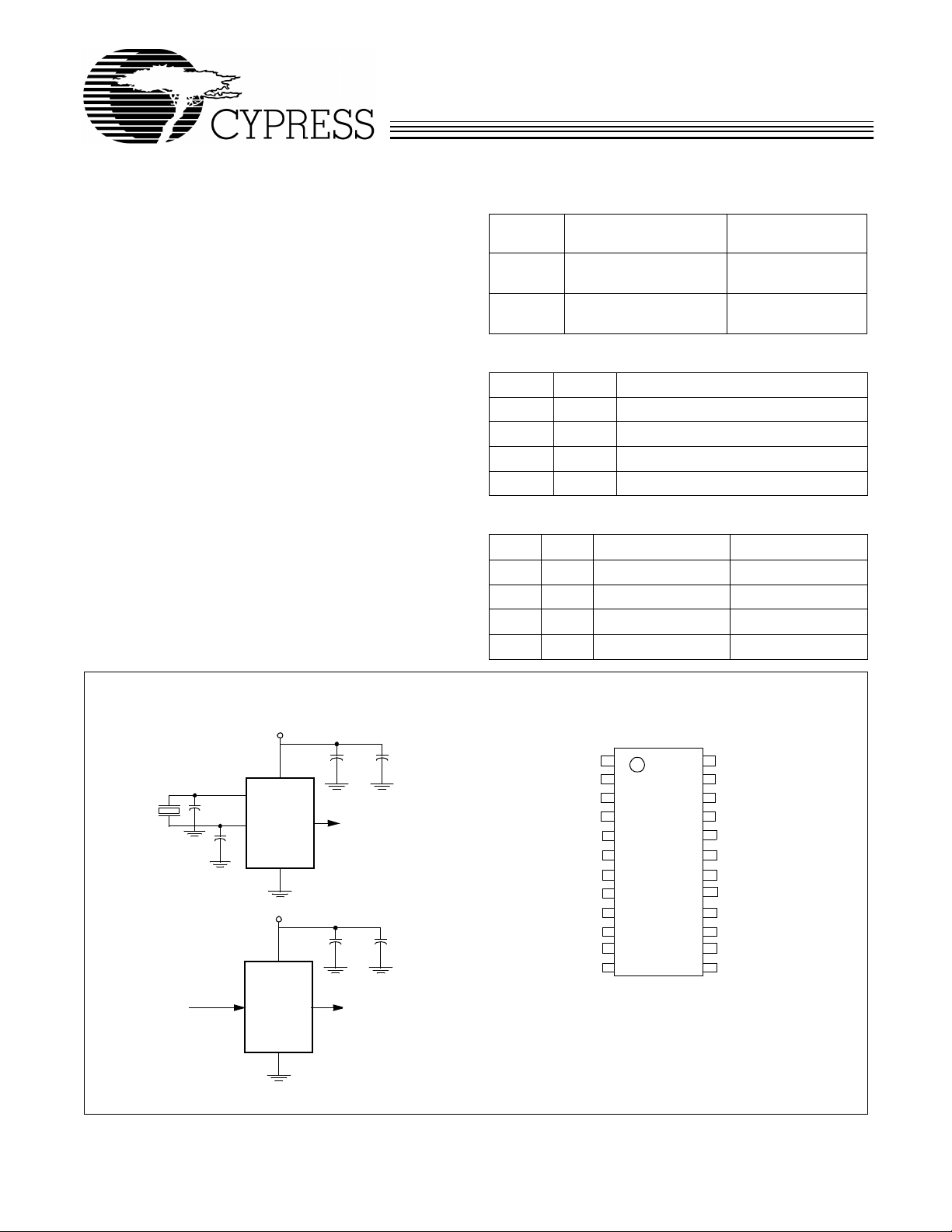
Simplified Block Diagram
3.3V or 5.0V
XTAL
Input
40MHz
max.
Oscillator or
Reference Input
PREMIS is a trademark of Cypress Semiconductor Corporation.
X1
X2
W185
3.3V or 5.0V
W185
Spread Spectrum
Output
(EMI suppressed)
Spread Spectrum
Output
(EMI suppressed)
Pin Configuration
SSOP
REFOUT
FS2
GND
SS%
EN2
GND
CLK0
VDD
CLK1
CLK2
X1
X2
1
2
3
4
5
6
7
8
9
10
11
12
24
23
W185/W185-5
22
21
20
19
18
17
16
15
14
13
SSON#
RESET
FS1
VDD
VDD
NC
EN1
CLK5
VDD
CLK4
GND
CLK3
Cypress Semiconductor Corporation
• 3901 North First Street • San Jose • CA 95134 • 408-943-2600
July 2 5, 2000, rev. *A
Page 2
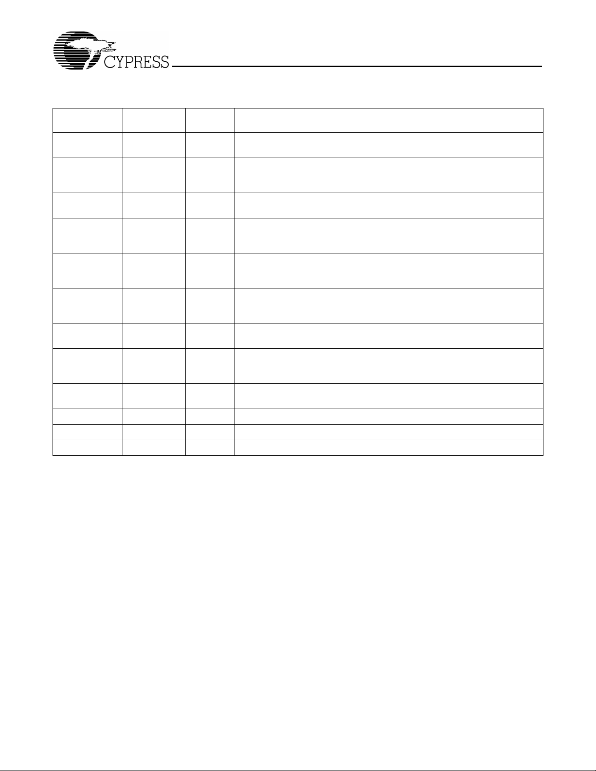
Pin Definitions
W185
Pin Name Pin No.
CLK0:5 9, 11, 12 , 13,
15, 17
CLKIN or X1 3 I
NC or X2 4 I
SS% 6 I
Reset 23 I
REFOUT 1 O
EN1:2 18, 7 I
SSON# 24 I
FS1:2 22, 2 I
VDD 10, 16, 20, 21 P
GND 5, 8, 14 G
NC 19 NC
Pin
Ty pe Pin Description
O
Modulated Frequency O utputs:
ulated input clock (SSON# asserted).
Crystal Connection or External Reference Frequency Input:
dual functions. It may ei ther be connected to an external crystal, or to an
external reference clock.
Crystal Connection:
connected.
Modulation Width Selection:
this pin is used to selec t t he am ount of v ariation and peak EM I r eduction that
is desired on the output signal. This pin has an int ernal pull-up resistor.
Modulation Profile Restart:
pattern at the begi nning of its de fined path . This pin has an internal pul l-do wn
resistor.
Non-Modulated Output:
This output will not have the Spread Spectrum feature enabled regardless of
the state of logic input SSON#.
Output Enable Select Pins:
buffers. See Table 3 on page 1.
Spread Spectrum Contro l (Active LOW):
turns the internal modul ation wav e f orm on. Thi s pin has an internal pul l-do wn
resistor.
Frequency Selection Bit 1 and 2:
tion. Refer to Table 1. These pins have internal pull-up resistors.
Po wer Connec tion:
Ground Conne ction:
No Connect:
This pin should be left float ing.
If using an external re ference, this pin must be left un-
This pin provides a copy of the ref erence frequ ency.
Connected to 3.3V or 5V po wer supply.
This should b e connected t o the common gr ound plane .
Fr equency modu lat ed copi es of th e unmod -
This pin has
When Spread Spectrum feature is turned on,
A rising edge on this input restarts the modulati on
These pins contr ol the act ivi ty of spec ifi c output
Asserting this signal (acti ve LOW )
These pins select the frequency of opera-
2
Page 3
W185
Overview
The W185 products are one series of devices in the Cypress
PREMIS family. The PREMIS family incorporates the latest
advanc es in PLL spread spectrum frequency synthesizer t echniques. By frequency modulating the output with a low-frequency carrier, peak EMI is greatly reduced. Use of this technology allows s ystems to pass increasingl y diff icult EMI testin g
without resorting to costly shielding or redesign.
In a system, not only i s EMI reduce d in the v arious cl oc k li nes,
but also in all signals which are synchronized to the clock.
Therefore, the benefits of using this technology increase with
the number of address and dat a lines in the syst em. The Simplified Block Diagram sho ws a simple implementa ti on.
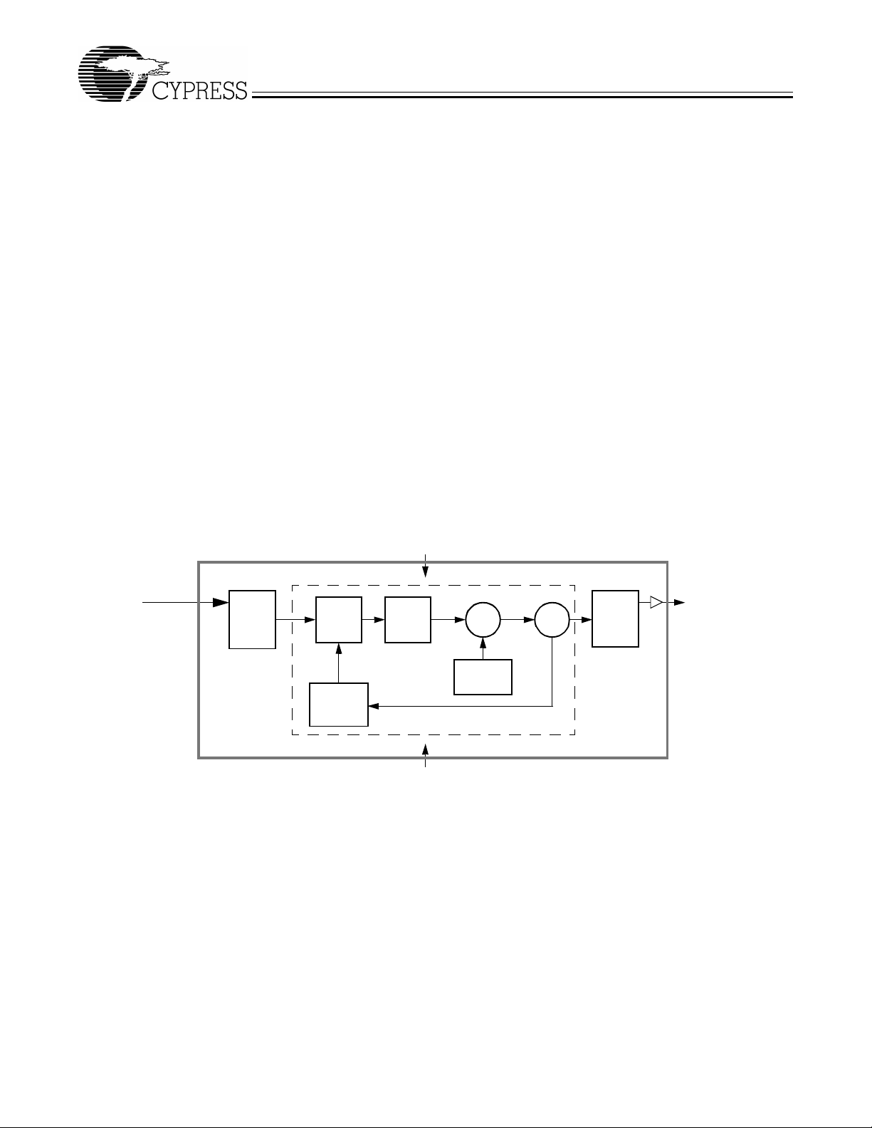
Functional Description
The W185 uses a Phase-Locked Loop (PLL) to frequency
modulate an input clock. The result is an output clock whose
frequency is slowly swept over a narrow band near the input
signal. The basic circuit topology is shown in Figure 1. The
input reference signal is divided by Q and fed to the phase
detector. A signal from the VCO is divided by P and fed back
to the phase detec tor als o . The PLL will f or ce the frequen cy of
the VCO output sign al to change until the divid ed output signal
and the divided reference signal match at the phase detector
input. The output frequency is then equal to the ratio of P/Q
times the ref er ence fre quenc y. (Note: Fo r the W 184 the ou tpu t
frequency is nominally equal to the input frequency.) The
unique feature of the Spread Spectrum Frequency Timing
Generator is that a modulating waveform is superimposed at
the input to th e VCO. This causes the VCO output to be s low ly
swept across a predetermined frequency band.
Because the modulating frequency is typically 1000 times
slower than the fundamental clock, the spread spectrum process has little impact on system performance.
Frequency Selection With SSFTG
In Spread Spectrum Frequency Timing Generation, EMI reduction depends on the shape, modulation percentage, and
frequency of the modulating waveform. While the shape and
frequency of the modulating waveform are fixed for a given
frequency, the modulation percent age m ay be varied .
Using frequency select bits (FS1:2 pins), the f requency range
can be set. Spreading percentage may be selected as either
1.25% or 3.75% (see Table 1).
A larger spreading per centage improv es EMI reduction. Ho w-
ever, large spread percentages may either exceed system
maximum frequ ency ra tings o r lo wer the a v er age fr eque ncy to
a point where performance is affected. For these reasons,
spreading percent age options are provided.
V
DD
Clock Input
Reference Input (EMI suppressed)
Freq. Phase
Q
Detector
Feedback
Divider
P
Charge
Pump
GND
Σ
Modulating
Waveform
VCO
PLL
Post
DividersDivider
CLKOUT
Figure 1. Functional Block Diagram
3
Page 4

W185
Spread Spectrum Frequency Timing
Generation
The device generates a clock that is frequency modulated in
order to increase the bandwidth that it occu pies. By increas ing
the bandwidth of the fundamental and its harmonics, the amplitudes of the radiated electromagnetic emissions are reduced. This effect is depicted in
As shown in
)LJXUH
, a harmonic of a modulated clock has a
much low er amplit ude than that of an un modulated si gnal. The
reduction in amplitude is dependent on the harmonic number
and the frequency deviation or spread. The equation for the
reduction is:
dB = 6.5 + 9*log
Amplitude (dB)
(P) + 9*log10(F)
10
SSFTG Typical Clock
)LJXUH
.
Where P is the pe rcentag e of de vi ation an d F is the frequency
in MHz where the reduction is measured.
The output clock is modulated with a waveform depicted in
)LJXUH
. This waveform, as discussed in “Spread Spectrum
Clock Gener ation f or the Redu ct ion of Radiat ed Emission s” by
Bush, Fessler, and Hardin produces the maximum reduction
in the amplitude of radiat ed electro magnetic emis sions.
details the Cypress spreading pattern. Cypress does offer
)LJXUH
options with more spread and greater EMI reduction. Contact
your local Sales representative for details on these devices.
EMI Reduction
Spread
Spectrum
Enabled
Amplitude (dB)
Non-
Spread
Spectrum
Frequency Span (MHz)
Center Spread
Frequency Span (MHz)
Down Spread
Figure 2. Clock Harmonic with and with out SSCG Modulati on Frequency Domai n Representat ion
MAX.
10%
20%
30%
40%
50%
60%
70%
80%
FREQUENCY
MIN.
90%
100%
10%
20%
30%
40%
50%
60%
70%
80%
Figure 3. Typical Modulation Profile
90%
100%
4
Page 5

Absolute Maximum Ratings
W185
Stresses greater than those listed in this table may cause permanent damage to the de vice . These represent a stress ratin g
only. Operation of the device at these or any other conditions
.
above those specified in the operating sections of t his specification is not implied. Maximum conditions for ex tended periods may affect reliability.
Parameter Description Rating Unit
V
, V
DD
IN
T
STG
T
A
T
B
P
D
DC Electr i cal C h ar acteristics
Voltage on any pin with respect to GND –0.5 to +7 .0 V
Storage Temperature –65 to +150 °C
Operating Temperature 0 to +70 °C
Ambient Temperature under Bias –55 to +125 °C
Power Dissipation 0.5 W
:
0°C < T
< 70°C, VDD = 3.3V ±5%
A
Parameter Description T est Condition Min. Typ. Max. Unit
I
DD
t
ON
V
IL
V
IH
V
OL
V
OH
I
IL
I
IH
I
OL
I
OH
C
I
R
P
Z
OUT
Note:
1. Inputs FS1:2 have a pull-up resistor; Input SSON# has a pull-down resistor.
Supply Current 18 32 mA
Power Up Time First locked clock c ycle after Power
5ms
Good
Input Low Voltage 0.8 V
Input High Voltage 2.4 V
Output Low Voltage 0.4 V
Output High Voltage 2.4 V
Input Low Current Note 1 –50 µA
Input High Current Note 1 50 µA
Output Low Current @ 0.4V, VDD = 3.3V 15 mA
Output High Current @ 2.4V, VDD = 3.3V 15 mA
Input Capacitance 7pF
Input Pull-Up Resistor 500 kΩ
Clock Output I mp edance 25 Ω
5
Page 6

W185
DC Electr i cal C h ar acteristics:
0°C < T
< 70°C, VDD = 5V ±10%
A
Parameter Description Test Condi ti on Min. Typ. Max. Unit
I
DD
t
ON
V
IL
V
IH
V
OL
V
OH
I
IL
I
IH
I
OL
I
OH
C
I
R
P
Z
OUT
AC Electrical Characteristics:
Supply Current 30 50 mA
Power Up Time First locked clock cycle after
5ms
Power Good
Input Low Voltage 0.15V
Input High Voltage 0.7V
DD
DD
Output Low Voltage 0.4 V
Output High Voltage 2.4 V
Input Low Current Note 1 –100 µA
Input High Current Note 1 50 µA
Output Low Current @ 0.4V, VDD = 5V 24 mA
Output High Current @ 2.4V, VDD = 5V 24 mA
Input Capacitance 7pF
Input Pull-Up Resistor 500 kΩ
Clock Output I mp edance 25 Ω
TA = 0°C to +70°C, VDD = 3.3V ±5% or 5V±10%
Symbol Parameter T est Condition Min. Typ. Max. Unit
f
OSC
f
IN
f
OUT
t
R
t
F
t
OD
t
ID
t
JCYC
EMI
RED
Internal Xtal Oscillator
Frequency
Input Frequency External reference 28 75 MHz
Output Frequency Spread Off, FS2:1 per
Output Rise Time 15-pF load 0.8V–2.4V 2 5 ns
Output Fall Time 15-pF load 2.4 –0.8V 2 5 ns
Output Duty Cycle 15-pF load 40 60 %
Input Duty Cycle 40 60 %
Jitter, Cycle-to-Cy c le 250 300 ps
Harmonic Reduction f
Xtal connected to X1, X2 28 40 MHz
28 75 M Hz
Table 2
= 40 MHz, thir d harmonic
out
8dB
measured, reference board,
15-pF load
t
SK
Output to Output Skew 300 ps
V
V
6
Page 7

W185
Application Information
Recommended Circuit Configuration
For optimum performance in system applications the power
supply decoupli ng scheme sho wn in Figure 4 should be used .
decoupling is important to both reduce phase jitter and
V
DD
EMI radiation. The 0.1-µF decoupling capacitor should be
placed as close to the V
Reference Output
XTAL Connection or
Clock Output
Clock Output
Clock Output
pin as possible, otherwise the in-
DD
R
Logic Input
Reference Input
XTAL Connection or NC
1
2
3
4
5
6
7
8
9
10
11
12
C1
0.1
R
R
µF
R
W185
24
23
22
21
20
19
18
17
16
15
14
13
3.3V or 5V System Supply
creased trace inductance will negate i ts decoupling capability.
The 10-µF decoupling capacitor shown should be a tantalum
type. For further EMI protection, the V
made via a ferrite bead, as shown.
connection can be
DD
Recommended Board Layout
Figure 5 shows a recommended 2-layer board layout.
C2
µF
NC
C3
0.1
Output
FB
Clock
Clock
Clock
Output
Output
C5
10
µF Tantalum
C4
0.1
µF
R
R
R
0.1
µF
Xtal Connection or Reference Input
Xtal Connec tion or NC
Clock Output
Power Supply Input
(3.3V or 5V)
G
R
C1
R
Figure 4. Recommended Circuit Configuration
C1....C4 =
C5 =
C2
G
G
FB
C5
C3
R
C4
R
G
G
G
G
G
R =
FB
G
Figure 5. Recommended Board Layout (2-Layer Board)
High frequency supply decoupling
capacitor (0.1-
Common supply low frequency
decoupling capacitor (10
recommended).
Match value to line impedance
=
Ferrite Bead
=
Via To GND Plane
µF recommended).
-µF tantalum
Ordering Information
Ordering Code
W185
W185-5
Document #: 38-00809-A
Package
Name
Package Type
H 24-Pin SSOP (209-mil)
7
Page 8

Package Diagram
E
D
C
B
A
W185
24-Pin Shrink Small Outli ne Package (SSOP, 209-m il )
87654321
ORIGINA TORDA TEDESCRIPTIONREV.
EXCELLENCE IN SEMICONDUCTOR
ASSEMBLY AND TEST
SHEETSCALE
1 of 2
06/13
HJC
1991
11/05
YMK
1992
11/08
EBA
1993
04/26
EBA
1994
06/19
EBA
1995
03/19
J.B.C.
1996
00 I NITIAL RELEASE PE R DCN#A33907.
01 RE VISED PER DCN#D20 214.
02 RE VISED PER DCN#D20 760.
03 RE VISED PER DCN#D21 151.
04 RE VISED PER DCN#D22 219.
05 RE VISED PER DCN#P60 056.
c
SECTION G-G
Anam Industrial Co., LTD.
Seoul, Korea
Amkor E lectron ics
Irving, TX Chandler, AZ
APPROVALS DATE
M. CHAVEZ
M. BANGLOY
H. BAUTISTA
H.J. CH OI
TITLE
6/13
1991
6/13
1991
6/13
A1
1991
6/13
1991
b1
8.
b
10.
Amkor/A na m Pilip in as, INC.
Manila, Ph ilippine s
Amkor Ele ctronic s
PACKAGE OUTLINE,
5.30mm (.209") BODY, SSOP
WITH LEAD FINISH
c1
BASE METAL
32289
P
I
N
E
S
-
DECIMAL
XX±
XXX±
XXXX±
MATERIAL
FINISH
DO NOT SCALE DRAWING
2.36
DIA. PIN
NOTES:
1. MAXIMUM DIE THICKNES S ALLOWABLE IS 0.43m m (.017 INCHES).
2.
DIMENSIONING & TOLERANCES PER ANSI.Y14.5M-1982.
3.
"T" IS A REFERENCE DATUM.
4.
"D" & "E" ARE REFERENCE DATUMS AND DO NOT
INCLUDE MOLD FLASH OR PROTRUSIONS, BUT
DO INCLUDE MOLD MISMATCH AND ARE MEASURED
AT THE PARTING LINE, MOL D FLASH OR
PROTRUSIONS SHALL NOT EXCEED 0 .15mm PER SIDE.
DIMENSION IS THE LENGTH OF TERMINAL
5.
FOR SOLDERING TO A SUBSTRATE.
TERMINAL POSITI ONS ARE SHOWN FOR REFERENCE ONLY.
6.
FORMED LEADS SHALL BE PLANAR WIT H RESPECT TO
7.
ONE ANOTHER WITHIN 0.0 8mm AT SEATING PLANE.
DIMENSION b DOES NOT INCLUDE DAMBAR PROTRUSION/INTRUSION.8.
ALLOWABLE DAMBAR PROTRUSION SHAL L BE 0.13mm TOTAL IN
EXCESS OF b DIMENSION AT MAXIMUM MATERIAL CONDITION.
DAMBAR INTRUSION SHALL NOT REDUCE DIMENSION b BY MORE
THAN 0.07mm AT LEAST MATER IAL CONDITION.
CONTROLLING DIMENSION: MILLIMETERS.9.
10. THESE D IMENSIONS APPLY TO THE FLAT SE CTION OF THE
LEAD BETWEEN 0.10 AND 0.2 5mm FROM LEAD TIPS.
THIS PACKAGE OUTLINE DRAWI NG COMPLIES WITH
11.
JEDEC SPECIFICATION NO. MO-150 FOR THE LEAD COUNTS SHOWN
PROJECTION
ANGULAR
±
DRAWN
CHECKED
ENG'R
RELEASED
1.00
1.00 DIA.
123
M+EM0.20
H
1.00
N
6
TOP VIEW
0° MIN.
SD0.12 M T E+
b
8
A
3
- T C0.076
7
SEATING
PLANE
L
5
DETAIL ' A '
.235 MIN
0.25 BSC
L1
SEE
DETAIL "A"
GAUGE PLANE
SEATING PLANE
A
1
R
e
- C -
-D4
SIDE VIEW END VIEW
PARTING LINE
G
C
OC
G
87654321
D/2
E/2
12-16°
A
2
P
I
L
I
H
P
BOTTOM VIEW
-E4
E
D
C
B
A
REV.DWG. NO.SIZE
05
87654321
THIS TABLE IN MILLIMETERS
S
E
D
Y
M
A
A
A
b
b1
c 0.09 0.20
c1 0.09 0.15 0.16
D
E
e
H
L
L1
N
R
C
S
Y
M
A
A
A
B
A
b
b1 .010 .012 .013
c .004 .008
c1 .004 .006 .0061010
D
E
e
H
L
L1 .049 REF.
N
O
R
87654321
COMMON
DIMENSIONS
B
O
L
1
2
CO
B
O
L
1
2
NOM.
MIN. MAX.
1.86
0.13
0.05
1.73 1.78
1.68
0.25 0.38
0.25 0.30 0.33
5.20 5.30 5.38
7.65
0.63 0.75
0.09
.068 .078
.002
.066
.010 .015
-
-
SEE VARIATIONS
0.65 BSC
7.80 7.90
1.25 REF.
SEE VARIATIONS
4°
0.15
COMMON
DIMENSIONS
NOM.
.073
.005
-
-
SEE VARIATIONS
.0256 BSC
.301
.030.025
SEE VARIATIONS
C
4°
0° 8°
.004
.006
N
VARI-
O
T
E
8,10
10
10
10
4
4
5
6
ATIONS
AA
AB
AC
AD
AE
AF
1.991.73
0.21
0.95
8°0°
THIS TABLE IN INCHES
NOTE 4
N
VARI-
O
T
E
8,10
10
4
4
5
6
ATIONS
AA
AB
AC
AD
AE
AF
MAX.MIN.
.008
.070.068
.212.209.205
.311.307
.037
4NOTE
D
MAX.MIN.
NOM.
6.07 6.20 6.33
6.07 6.20 6.33
7.07 7.20 7.33
8.07 8.20 8.33
10.07 10.20 10.33
10.07 10.20 10.33
IS DESIGNED BUT NOT TOOLED
D
NOM.
MIN. MAX.
.249.244.239
.249.244.239
.289.284.278
.328.323.318
.407.402.397
.407.402.397
6
N
14
16
20
24
28
30
VARIATION AF
6
N
14
16
20
24
28
30
TITLE
5.30mm ( .209") BODY, SSOP
A1
8/1
PACKAGE OUTLINE,
32289
SHEETSCALE
2 of 2
E
D
C
B
A
REV.DWG. NO.SIZE
05
© Cypress Semiconductor Corporation, 2000. The information contained herein is subject to change without notice. Cypress Semiconductor Corporation assumes no responsibility for the use
of any circuitry other than circuitry embodied in a Cypress Semiconductor product. Nor does it conv ey or imply any lice nse under patent or other rights. Cypress Semicondu ctor does not authorize
its products for use as critical components in life-support systems where a malfunction or failure may reasonably be expected to result in significant injury to the user. The inclusion of Cypress
Semiconductor products in life-support systems application implies that the manufacturer assumes all risk of such use and in doing so indemnifies Cypress Semiconductor against all charges.
 Loading...