

Page 1
PRELIMINARY
133-MHz Spread Spectrum FTG f or Pentium® II Plat f orms
W167B
Cypress Semiconductor Corporation
• 3901 North First Street • San Jose • CA 95134 • 408-943-2600
November 2, 1999
Features
• Maximized EMI Suppression usi ng Cypress’s Spread
Spec t r u m techno logy
• Three copies of CPU outputs select able frequency
• Three copies of 3V66 selectable frequency out put at
3.3V
• T en copies of PCI clocks (select able frequency), 3.3V
• One double strength 14. 318-MHz reference output at
3.3V
• One copy of 48-MHz USB clock
• One copy of selectabl e 24-/48-MHz for SIO
• One copy of CPU- divide-b y-2 output as refer ence input
to Direct Rambus™ Clock Generator ( C ypress W134)
• Three copies of IO APIC
• Av ail able in 48-pin SSOP (300 mils)
Key Specific ati o n s
Supply Voltages:...................................... V
DDQ2
= 2.5V±5%
V
DDQ3
= 3.3V±5%
CPU, CPUdiv2 Output Jitter:............ .. .........................250 ps
CPU, CPUdiv2 Outp ut Skew:................... ................ ... 175 ps
IOAPIC, 3V66 Output Skew: . ...................................... 250 ps
PCI0:8 Pin to Pin Ske w:................... .. ............. .. .. ........500 ps
Duty Cyc l e: ...... ................... ... .. .......... .. ... ......... ... .. ..... 45/5 5 %
Spread Spectrum Modulation:................................... ±0.25%
CPU to 3V66 Output Offset:............ .0.0–1.5 ns (CPU leads)
3V66 to PCI Output Offset:.............. 1.5–4.0 ns (3V66 leads)
CPU to IOAPIC Output Offset:.........1.5–4.0 ns (CPU leads)
Direct Rambus is a trademark of Rambus, Inc. Pentium is a registered trademark of Intel Corporation.
T able 1. Pin Selectable Frequency
SEL133/
100# SEL2 SEL1 SEL0
CPU
MHz
3V66
MHz
PCI
MHz
IOAPIC
MHz
1 1 1 1 133.3 66.7 33.3 16.7
1 1 1 0 138 69 34.5 17.3
1 1 0 1 143 71.5 35.8 17.9
1 1 0 0 148 74 37 18.5
1 0 1 1 150 75 37.5 18.8
1 0 1 0 152.5 76.3 38.1 19.1
1 0 0 1 155 77.5 38.8 19.4
1 0 0 0 160 80 40 20
0 1 1 1 100.2 66.8 33.4 16.7
0 1 1 0 105 70 35 17.5
0 1 0 1 114 76 38 19
0 1 0 0 120 80 40 20
0 0 1 1 66.8 66.8 33.4 16.7
0 0 1 0 124 82.7 41.3 20.7
0 0 0 1 128.5 64.3 32.1 16.1
0 0 0 0 133.9 67 33.5 16.7
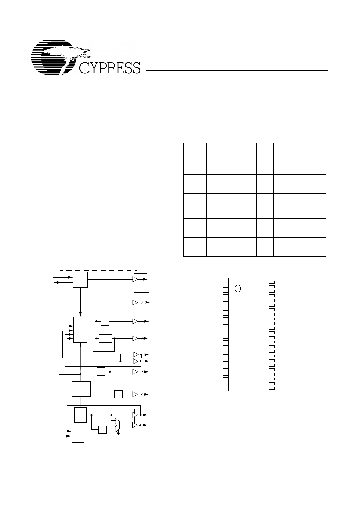
Block Diagram
Pin Configuration
Note:
1. Internal 250-kΩ pull-up resistors present on inputs marked with *.
Design should not rely solely on internal pull-up resistor to set I/O
pins HIGH.
[1]
REF2X
CPU_[0:2]
CPUdiv2
3V66_[0:2]
XTA L
PLL 1
X2
X1
PCI_[2:9]
IOAPIC[0:2]
48MHz/SEL0*
PLL2
OSC
÷2
Power
÷2/÷1.5
Down
Logic
÷2
÷2
3
3
PWRDWN#
3
÷2
SIO/24_48#MHz
Serial
Logic
SEL133/100#
SCLK
SDATA
PCI0/SEL2*
PCI1/SEL1*
8
IOAPIC2
REF2X
VDDQ3
X1
X2
GND
SEL2*/PCI0
SEL1*/PCI1
VDDQ3
PCI2
PCI3
PCI4
PCI5
GND
PCI6
PCI7
VDDQ3
PCI8
PCI9
GND
3V66_0
3V66_1
3V66_2
VDDQ3
W167B
GND
VDDQ2
IOAPIC0
GND
VDDQ2
CPUdiv2
GND
VDDQ2
CPU2
GND
VDDQ2
CPU1
CPU0
SDATA
VDDQ3
GND
PWRDN#*
SCLK
VDDQ3
SIO/24_48#MHz
*
48MHz/SEL0*
GND
SEL133/100#
48
47
46
45
44
43
42
41
40
39
38
37
36
35
34
33
32
31
30
29
28
27
26
25
1
2
3
4
5
6
7
8
9
10
11
12
13
14
15
16
17
18
19
20
21
22
23
24
IOAPIC1
Q#
VDDQ3
VDDQ2
VDDQ3
VDDQ2
VDDQ3
Page 2
W167B
PRELIMINARY
2
Pin Definitions
Pin Name
Pin
No.
Pin
Type Pin Description
CPU0:2 35, 36, 39 O
CPU Clock Outputs 0 through 2:
CPU clock outputs. Their output voltage
swing is controlled by voltage applied to VDDQ2.
SEL133/100# 25 I
SEL133/100#:
Frequen cy selection input pin as shown in Table 1.
PCI0/SEL2 7 I/O
PCI Clock Output 0 and Selection Bit 2:
As an output, this pin works in
conjunctio n wit h PCI2:9. When an input, this pin functions as part of the frequency selecti on address (see Table 1).
PCI1/SEL1 8 I/O
PCI Clock Output 1 and Selection Bit 1:
As an output, this pin works in
conjunctio n wit h PCI2:9. When an input, this pin functions as part of the frequency selecti on address (see Table 1).
PCI2:9 10, 11, 12,
13, 15, 16,
18, 19
O
PCI Clock Outputs 2 t hrough 9 :
Output vol tage swi ng is cont rolled b y volt age
applied to VDDQ3.
3V66_0:2 21, 22, 23 O
66-MHz Clock Outputs 0 through 2:
Output voltage s wing is controlled by
voltage app li ed to VDDQ3.
CPUdiv2 42 O
CPU-Divide-By-2 Output:
This serves as a reference input signal for Direct
Rambus
Clock Generator (Cypress W134). The output voltage is determined
by VDDQ2.
IOAPIC0:2 46, 45, 1 O
I/O APIC Clock Output 0 through 2:
Provide outputs synchronous to CPU
clock. See Table 1 and Table 5 for their relat ion to other system cloc k outputs.
48MHZ/SEL0 27 I/O
48-MHz Output and Selection Bit 0:
Fixed clock output that defaults to
48-MHz f ollo win g de vi ce po wer -up . When an i nput , t his pin f unc tions as pa rt of
the frequency sel ection address (see Table 1).
SIO/24_48#MHz 28 I/O
Super I/O Referen ce Clock Out put and SIO Clo ck Frequenc y Select:
Fixed
clock outpu t that pr ovi des the reference input clock to a Super I/O de vi ce. The
output freque ncy is det ermined by t he input valu e on this pi n during po wer up .
If input is sampled HIGH, the output operat es at 24 MHz, otherwise, the output
operates at 48 MHz.
REF2X 2 O
Fixed 14.318-MHz Output:
With double strength driving capability.
PWRDWN# 31 I
Power Down Control
X1 4 I
Crystal Connection or External Reference Frequency Input:
This pin has
dual functions . It can b e used as an e xternal 14.318 -MHz crystal conn ection or
as an external reference frequency input.
X2 5 I
Crystal Connection:
An input con necti on f or an ext ernal 14 .31 8-MHz crysta l.
If using an ex ternal reference, this pin must be left unconnected.
SDATA 34 I/O
Serial Data Input:
Data input for Serial Data Interface. Refer to Serial Data
Interface s ec ti o n tha t follo w s.
SCLK 30 I
Serial Clock Input:
Clock input for Serial Data Interface. Refer to Serial Data
Interface s ec ti o n tha t follo w s.
VDDQ2 37, 40, 43, 47 P
Power Connection:
Connected to 2.5V power supply.
VDDQ3 3, 9, 17, 24,
29, 33
P
Power Connection:
Connected to 3.3V supply.
GND 6, 14, 2 0, 26,
32, 38, 41,
44, 48
G
Ground Connecti on:
Connect all ground pins to the common system ground
plane.
Page 3
W167B
PRELIMINARY
3
Overview
The W167B, a motherboard clock synthesizer, provides 2.5V
CPU clock outputs for advanced CPU and a CPU-divide-by-2
refere nce frequency for Di rect Rambus
Clock Generat or (such
as Cypress W134) i nterf ace. Fix ed ou tput frequenci es are provided for other system functions.
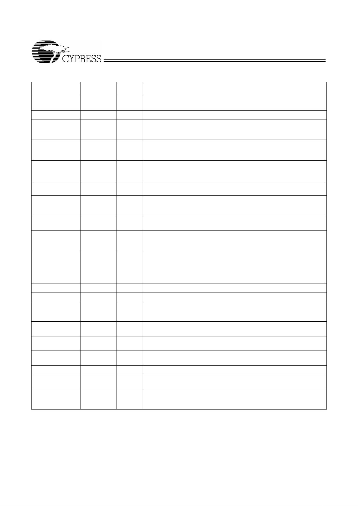
I/O Pin Operation
Pins 7, 8, 27, and 28 are dual-purpose l/O pins. Upon powerup these pins act as log ic in puts, all owing the det erminatio n of
assigned device functions. A short time after power -up, the
logic state of these pins is latched and the pins then become
clock outputs. This feature reduces device pin count by combining cloc k outputs with input selec t pi ns.
An external 10-kΩ “strapping” resistor is connected between
each l/O pin and ground or V
DD3
. Connection to gr ound s ets a
latch to “0”, connection to V
DD3
sets a latch to “1”. Figure 1 and
Figure 2 show two suggested methods for strapping resistor
connection.
Upon W167B power up, the first 2 ms of operation is used for
input logic selection. During this period, these dual-purpose
I/O pins ar e three-s tated, all owing the output st rapping resi stor
on each l/O pin to pull the pin and its associated capacitive
clock load to either a logic HIGH or LOW state. At the end of
the 2-ms period, the establi shed logic 0 or 1 condition of each
l/O pin is then latched. Next, the output buffers are enabled,
converting the l/O pins into ope rating clock outputs. The 2-ms
timer starts when V
DD
reaches 2.0V. The input bits can only
be reset by turning V
DD
off and then back on again.
It should be noted that the strapping resistors have no significant effect on clock output signal integrity. The drive impedance of the c lock out puts is <40 Ω (nominal) which is minimally
affected by the 10-kΩ strap to ground or V
DD
. As with the series termination resistor, the output strapping resistor should
be placed as close to the l/O pin as possible in order to keep
the interconnecting trace short. The trace from the resistor to
ground or V
DD
should be ke pt less t han tw o i nches i n lengt h to
prevent system noise coupling during input logic sampling.
When the clock out puts are enabled following the 2-ms input
period, target ( normal) output f requenc y is deliv ered a ssuming
that V
DD
has stabilized. If VDD has not yet reached full value,
output frequency in iti ally ma y be below t arget b ut wil l in crease
to target once V
DD
voltage has stabilized. In either case, a
short output clock cycle may be produced from the CPU clock
outputs when the outputs are enabled.
Power-on
Reset
Timer
Output Three-state
Data
Latch
Hold
QD
W167B
V
DD
Clock Load
R
10 k
Ω
Output
Buffer
(Load O ption 1)
10 k
Ω
(Load O ption 0)
Output
Low
Output Strapping Resistor
Series Termination Resistor
Figure 1. Input Logic Selection Through Resistor Load Option
Power-on
Reset
Timer
Output Three-state
Data
Latch
Hold
QD
W167B
V
DD
Clock Load
R
10 k
Ω
Output
Buffer
Output
Low
Output Strapping Resistor
Series Termination Resistor
Jumper Options
Figure 2. Input Logic Selection Through Jumper Option
Page 4

W167B
PRELIMINARY
4
CPU/PCI Freq uency Selection
CPU frequency is selected wi th I/O pins 7, 8, 27, (SEL 2/PCI 0,
SEL1/PCI1, 48MHz/SEL0, respectively) and input pin 25
(SEL133/100#). Refer to Table 1 for CPU/PCI frequency pro-
gramming information. Additional frequency selections are
ava il able through th e seri al data interface. Refer to Table 5 on
page 9.
Output Buffer Configuration
Clock Output s
All clock outputs are designed to drive serial terminated clock
lines. The W167B outputs are CMOS-type which provide railto-rail output swing.
Crystal Oscillator
The W167B requires one input reference clock to synthesize
all output frequencies. The reference clock can be either an
externally gener ated cloc k signal or the cloc k generat ed by the
internal crystal oscil lator. When using an e x ternal clo c k sig nal,
pin X1 is used as the clock in put and pin X2 is left open.
The internal crystal oscillator is used in conjunction with a
quartz crystal connected t o de vi ce pins X 1 and X2 . Th is f orms
a parallel resonant crystal oscil lator circuit. The W167B incorporates the necessary feedback resistor and crystal load capacitors. Including typical stray circuit capacitance, the total
load presented to the crystal is approximately 18 pF. For optimum frequency accuracy without the addition of external capacitors, a parallel-resonant mode crystal s pecifying a load o f
18 pF should be used. This will typically yield reference frequency accuracies within ±100 ppm.
Page 5
W167B
PRELIMINARY
5
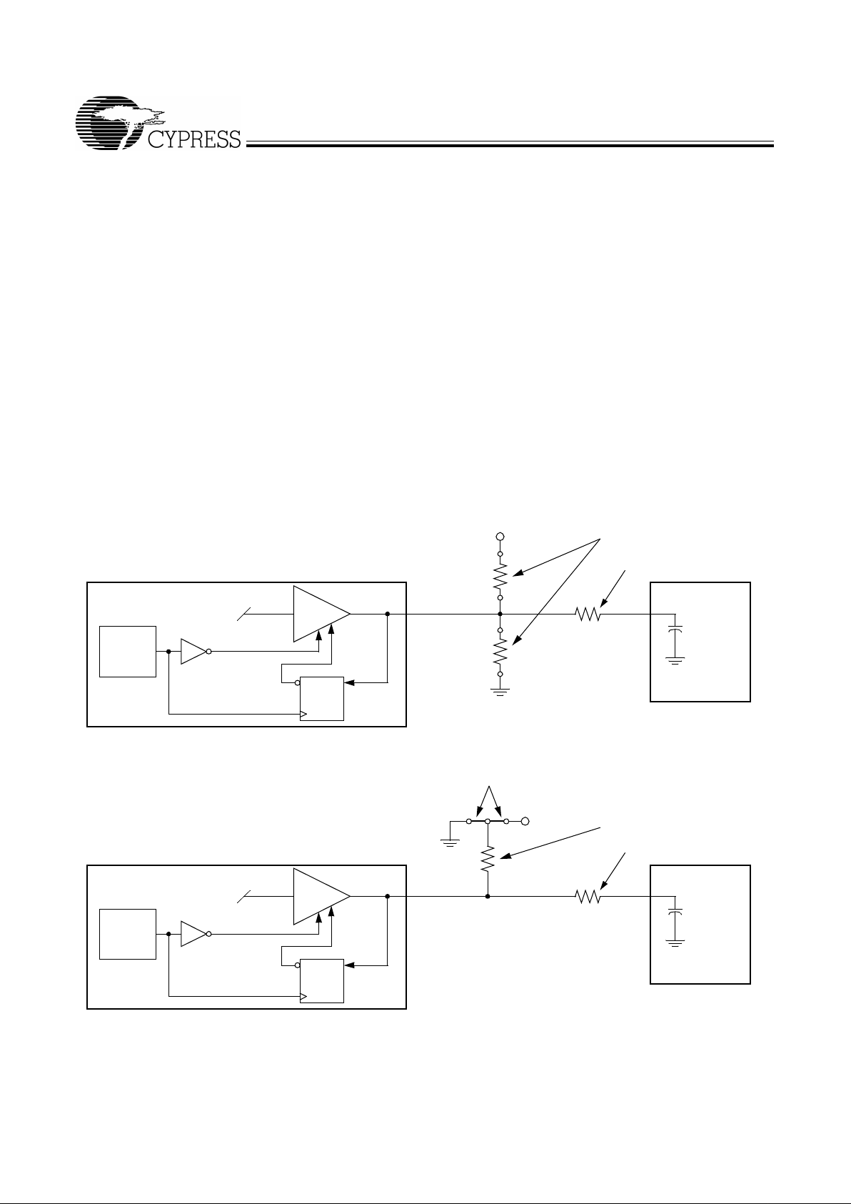
Spread Sp ectrum Feat u re
The device generates a clock that is frequency modulated in
order to increase the bandwidth that it occu pies. By increas ing
the bandwidth of the fundamental and its harmonics, the amplitudes of the radiated electromagnetic emissions are reduced. This effect is depicted in Figure 3.
As shown in Figure 3, a harmonic of a modulated cl ock has a
much low er amplitude th an that of an un modulated si gnal. The
reduction in amplitude is dependent on the harmonic number
and the frequency deviation or spread. The equation for the
reduction is
dB = 6.5 + 9*log
10
(P) + 9*log10(F)
Where P is the perce nta ge of de viati on and F is the frequen cy
in MHz where the reduction is measured.
The output clock is modulated with a waveform depicted in
Figure 4. This waveform, as discussed in “Spread Spect rum
Clock Generation f or the Reducti on of Radiated Emissio ns” by
Bush, Fessler, and Hardin produces the maximum reduction
in the amplitude of radiated electromagnetic emissions. The
deviati on selec ted for this chip i s –0.5% do wnspr ead. Fi gure 4
details the Cypress spr eading pat tern. Cypress does offer options with more spread and greater EMI reduction. Cont act
your local Sales representative for details on these devices .
Spread
Spectrum
Enabled
EMI Reduction
Spread
Spectrum
Non-
Figure 3. Typical Clock and SSFTG Comparison
100%
60%
20%
80%
40%
0%
–20%
–40%
–60%
–80%
–100%
10%
20%
30%
40%
50%
60%
70%
80%
90%
100%
10%
20%
30%
40%
50%
60%
70%
80%
90%
100%
Time
Frequency Shift
Figure 4. Typica l Modulation Profile
Page 6
W167B
PRELIMINARY
6
Serial Data Interface
The W167B features a two-pin, serial data interface that can
be used to configure internal register settings that control particular device functions. Upon power-up, the W167B initializes
with default register settings, therefore the use of this serial
data interface is optional. The serial interface is write-only (to
the clock chip) and is the dedicated function of device pins
SDATA and SCLOCK. In motherboard applications, SDATA
and SCLOCK are typically driven by two logic outputs of the
chipset. Clock device register changes are normally made
upon system initialization, if any are required. The interface
can also be used duri ng system oper ation for po wer management functions. Ta b le 2 summarizes the control functions of
the serial data interface.
Operation
Data is written to the W167B in ten bytes of eight bits each. Byte s are written in the order shown in Table 3.
T able 2. Serial Data Interface Control Functions Summary
Control Function Description Common Application
Clock Output Disable Any individual clock output(s) can be disabled. Di s-
abled outputs ar e actively held LO W.
Unused outputs are di sabled to reduce EMI
and system power. Examples are clock outputs to unused SDRAM DIMM socket or PCI
slot.
CPU Clock Frequency
Selection
Provides CPU/PCI freque ncy selections. Frequency is changed in a smooth and controlled fashion.
For alternate CPU devi ces, and pow er management options. Smooth frequency transition allows CPU fr equency ch ange un der nor-
mal system operati on.
Output Three-state Puts all clock outputs into a high-impedance state. Production PCB testing.
Test Mode All clock outputs toggle in relation with X1 input ,
internal PLL is bypassed. Refer to Tabl e 4.
Production PCB testing.
(Reserved) Reserved function for future device revision or pro-
duc tion device testing.
No user application . Regist er bit must be wri t-
ten as 0.
Table 3. Byte Writing Sequence
Byte Sequence Byte Name Bit Sequence Byte Description
1 Slave Address 11010010 Commands the W167B to acce pt the bi ts i n Data Byte s 0–6 f or internal
register configuration. Since other devices may exist on the s am e com mon serial data b us, i t is neces sary to ha ve a sp eci fic s lav e address for
each potential receiver. The slave receiver address f or the W167B is
11010010. Register sett ing will not be made if t he Slav e Address is not
correct (or is f or an alternate slave receiver).
2 Command
Code
Don’t Care Unused by the W167B, th erefore b it values ar e ignored (d on’t care). This
byte must be included in the data write seq uence to mai ntain proper b yte
allocation. The Command Code Byte is part of the st and ard serial communication protocol and may be used when writing to another addressed slave receiver on the serial data bus.
3 Byte Count Don’t Care Unused by the W167B, th erefore b it valu es are ignored (d on’t care). This
byte must be included in the data write seq uence to mai ntain proper b yte
allocation. The Byte Count Byte is part of the standard serial communication protocol and may be used when writing to another addressed
slave receiver on the serial dat a bus.
4 Data Byte 0 Refer to Table 4 The data bits in these bytes set internal W167B registers that control
device operation. The data bits are only accepted when the Address
Byte bit sequence is 11010010, as noted above. For description of bit
control functions, refer to Table 4, Data Byte Serial Configuration Map.
5 Data Byte 1
6 Data Byte 2
7 Data Byte 3
8 Data Byte 4
9 Data Byte 5
10 Data Byte 6
Page 7

W167B
PRELIMINARY
7
Writing Data Bytes
Each bit in the data bytes control a particular device function
except for the “reserved” bits which must be written as a logic
0. Bits are written MSB (most significant bit) first, which is bit
7. Ta b l e 4 gives the bit formats for registers located in Data
Bytes 0–6. Table 5 details additional frequency selections that
are available through the serial data interface. Ta ble 6 de t ail s
the select functions for Byte 0, bits 1 and 0.
Table 4. Data Bytes 0–6 Seri al Conf iguration Map
Bit(s)
Affected Pin
Control Function
Bit Control
DefaultPin No. Pin Name 0 1
Data Byte 0
7 -- -- SEL133/100# Refer to Table 5 0
6 -- -- SEL2 Refer to Table 5 0
5 -- -- SEL1 Refer to Table 5 0
4 -- -- SEL0 Refer to Table 5 0
3 -- -- Frequency Table Selection Controlled b y exter-
nal pin (per Table 1)
Controlled b y BYTE0
(per Table 5)
0
2-- --(Reserved) -- -- 0
1 - 0 -- -- Functional control Refer to Table 6 00
Data Byte 1
7 27 48MHz Clock Output Disable Low Active 1
6 28 24/48MHz Clock Output Disable Low Active 1
5-- --(Reserved) -- -- 0
4 42 CPUdiv2 Clock Output Disable Low Active 1
3-- --(Reserved) -- -- 0
2 39 CPU2 Clock Output Disable Low Active 1
1 36 CPU1 Clock Output Disable Low Active 1
0 35 CPU0 Clock Output Disable Low Active 1
Data Byte 2
7 16 PCI7 Clock Output Disable Low Active 1
6 15 PCI6 Clock Output Disable Low Active 1
5 13 PCI5 Clock Output Disable Low Active 1
4 12 PCI4 Clock Output Disable Low Active 1
3 11 PCI3 Clock Output Disable Low Active 1
2 10 PCI2 Clock Output Disable Low Active 1
1 8 PCI1 Clock Output Disable Low Active 1
0 7 PCI0 Clock Output Disable Low Active 1
Data Byte 3
7-- --(Reserved) -- -- 0
6 23 3V66_2 Clock Output Disable Low Active 1
5 22 3V66_1 Clock Output Disable Low Active 1
4 21 3V66_0 Clock Output Disable Low Active 1
3-- --(Reserved) -- -- 0
2-- --(Reserved) -- -- 0
1 19 PCI9 Clock Output Disable Low Active 1
0 18 PCI8 Clock Output Disable Low Active 1
Page 8

W167B
PRELIMINARY
8
Data Byte 4
7-- --(Reserved) -- -- 0
6 1 I OAPIC2 Clock Output Disable Low Active 1
5 45 IOAPIC1 Clock Output Disable Low Active 1
4 46 IOAPIC0 Clock Output Disable Low Active 1
3-- --(Reserved) -- -- 0
2-- --(Reserved) -- -- 0
1-- --(Reserved) -- -- 0
0 2 REF2X Clock Output Disable Low Active 1
Data Byte 5
-- -- -- (Reserved) -- -- 0
-- -- -- (Reserved) -- -- 0
-- -- -- (Reserved) -- -- 0
-- -- -- (Reserved) -- -- 0
-- -- -- (Reserved) -- -- 0
-- -- -- (Reserved) -- -- 0
-- -- -- (Reserved) -- -- 0
-- -- -- (Reserved) -- -- 0
Data Byte 6
-- -- -- (Reserved) -- -- 0
-- -- -- (Reserved) -- -- 0
-- -- -- (Reserved) -- -- 0
-- -- -- (Reserved) -- -- 0
-- -- -- (Reserved) -- -- 0
-- -- -- (Reserved) -- -- 0
-- -- -- (Reserved) -- -- 0
-- -- -- (Reserved) -- -- 0
Table 4. Data Bytes 0–6 Seri al Conf iguration Map
(continued)
Bit(s)
Affected Pin
Control Function
Bit Control
DefaultPin No. Pin Name 0 1
Page 9

W167B
PRELIMINARY
9
Note:
2. CPU, IOAPIC, and PCI frequency selections are listed in
Table 1
and
Table 5
.
T able 5. Additional Frequency Selections through Serial Data Interface Data Bytes
SEL133/100# SEL2 SEL1 SEL0
CPU
MHz
3V66
MHz
PCI
MHz
IOAPIC
MHz
1 1 1 1 133.3 66.7 33.3 16.7
1 1 1 0 138 69 34.5 17.3
1 1 0 1 143 71.5 35.8 17.9
1 1 0 0 148 74 37 18.5
1 0 1 1 150 75 37.5 18.8
1 0 1 0 152.5 76.3 38.1 19.1
1 0 0 1 155 77.5 38.8 19.4
1 0 0 0 160 80 40 20
0 1 1 1 100.2 66.8 33.4 16.7
0 1 1 0 105 70 35 17.5
0 1 0 1 114 76 38 19
0 1 0 0 120 80 40 20
0 0 1 1 66.8 66.8 33.4 16.7
0 0 1 0 124 82.7 41.3 20.7
0 0 0 1 128.5 64.3 32.1 16.1
0 0 0 0 133.9 67 33.5 16.7
T able 6. Select Function for Data Byte 0, Bits 0:1
Function
Input Conditions Output Conditions
Data Byte 0
CPU0:2, PCI0:9 REF2X IOAPIC0:2 48/24MHZBit 1 Bit 0
Normal Operation 0 0 Note 2 Note 2 14.318 MHz Note 2 48/24 MHz
Test Mode 0 1 TBD TBD TBD TBD TBD
Spread Spectrum 1 0 ±0.25% ±0.25% 14.318 MHz ±0.25% 48/24 MHz
Three-state 1 1 Hi-Z Hi-Z Hi-Z Hi-Z Hi-Z
Page 10

W167B
PRELIMINARY
10
How To Use the Serial Data Interface
Electrical Requirements
Figure 5 illust rat es el ectrical ch aract eristi cs for the serial interface bus used with the W167B. Dev ices send data ov er the bus
with an open drain logic output that can (a) pull the bus line
LOW, or (b) let the bus default to logic 1. The pull-up resistors
on the bus (both clock and data lines) establish a default logic
1. All bus de vices generally have logic i nputs to receive data.
Although the W167B is a receive- only device (no data writeback capa bil ity), it does transmit an “acknowledge” data pulse
after each byte is received. Thus, the SDATA line can both
transmit and receive data.
The pull-up resistor should be sized to meet the rise and fall
times specif ied i n A C p aramete rs , ta king i nto con si derat ion total bus line cap acitance.
DATA IN
DATA OUT
N
CLOCK IN
CLOCK OUT
CHIP SET
(SERIAL BUS MASTER TRANSMITTER)
SDCLK SDATA
SERIAL BUS CLOCK LINE
SERIAL BUS DATA LINE
N
DATA IN
DATA OUT
CLOCK IN
CLOCK DEVICE
(SERIAL BUS SLAVE RECEIVER)
SCLOCK SDATA
N
~ 2k
Ω
~ 2k
Ω
VDD VDD
Figure 5. Serial Interface Bus Electrical Characteristics
Page 11

W167B
PRELIMINARY
11
Sign aling R equire m ents
As shown in Fi gure 6, v alid dat a bits are def ined as st able logic
0 or 1 condi tion on the data line during a clock HIGH (logic 1)
pulse. A transi tio ning dat a line duri ng a cloc k HIGH pulse may
be interpreted as a start or stop pulse (it will be interpreted as
a start or stop pulse if the start/stop timing parameters are
met).
A write sequence is i nitiat ed b y a “start bit” as show n in Figure
7. A “stop bit” signifies that a transmission has ended.
As stated previously, the W167B sends an “acknowledge”
pulse after receiving eight data bits in each byte as shown in
Figure 8.
Sending Data to the W167B
The device accepts data once it has detected a valid start bit
and address byte sequence. Device functionality is changed
upon the receipt of each dat a bit (regist ers are not doub le buff ered). Partial transmiss ion is allo wed meaning that a transmis sion can be truncated as soon as the desired data bits are
transmitte d (remaining register s will be unmodifi ed). Transmission is truncated with either a stop bit or new start bit (restart
condition).
SDATA
SCLOCK
Valid
Data
Bit
Change
of Data Allowed
Figure 6. Serial Data Bus Valid Data Bit
SDATA
SCLOCK
Start
Bit
Stop
Bit
Figure 7. Serial Data Bus Start and Stop Bit
Page 12

W167B
PRELIMINARY
12
MSB
12345678A12345678A 1234SCLOCK 12345678A
11010010 LSB MSB MSB LSBSDATA
SDATA
Signaling from System Core Logic
Start Condition
MSB LSB
Slave Address
(First Byte)
Command Code
(Second Byte)
Last Data Byte
(Last Byte)
Byte Count
(Third Byte)
Stop Condition
Signaling by Clock Device
Acknowledgment Bit
from Clock Device
Figure 8. Ser ial Data Bus Write Sequence
t
STHD
t
LOW
t
R
t
HIGH
t
F
t
DSU
t
DHD
t
SP
t
SPSUtSTHD
t
SPSU
t
SPF
SDATA
SCLOCK
Figure 9. Serial Dat a Bus Timing Di agram
Page 13

W167B
PRELIMINARY
13
Absolute Maximum Ratings
Stresses gre ater th an those list ed i n this tab le may cause permanent damage to the de vice. These represent a str ess ratin g
only. Operation of the device at these or any other conditions
above those specified in the operatin g sections of this specification is not implied. Maximum conditions for extended periods may affect reliability.
.
Parameter Description Rating Unit
V
DD
, V
IN
V oltage on any pin with respect to GND –0.5 to +7 .0 V
T
STG
Storage Temperature –65 to +150 °C
T
A
Operating Temperature 0 to +70 °C
T
B
Ambient Temperature under Bias –55 to +125 °C
ESD
PROT
Input ESD Protection 2 (min.) kV
DC Electr i cal C h ar acteristics :
TA = 0°C to +70°C, V
DDQ3
= 3.3V±5%, V
DDQ2
= 2.5V±5%
Parameter Description Tes t Condi ti on Min. Typ. Max. Unit
Supply Current
I
DD-3.3V
Combined 3.3V Supply Current CPU0:3 =133 MHz
[3]
160 mA
I
DD-2.5
Combined 2.5V Supply Current CPU0:3 =133 MHz
[3]
90 mA
Logic Inputs (All referenced to V
DDQ3
= 3.3V)
V
IL
Input Low V oltage GND –
0.3
0.8 V
V
IH
Input High V oltage 2.0 VDD +
0.3
V
I
IL
Input Low Current
[4]
–25 µA
I
IH
Input High Current
[4]
10 µA
I
IL
Input Low Current, SEL133/100#
[4]
–5µA
I
IH
Input High Current, SEL133/100#
[4]
5µA
Clock Outputs
CPU, CPUdiv2, IO APIC (Referenced to V
DDQ2
) Test Condition Min. Typ. Max. Unit
V
OL
Output Low Voltage IOL = 1 mA 50 mV
V
OH
Output High Voltage IOH = –1 mA 2.2 V
I
OL
Output Low Current V
OL
= 1.25V 45 65 100 mA
I
OH
Output High Current VOH = 1.25V 45 65 100 mA
48MHz, RE F (R eferen ced to V
DDQ3
) Tes t Condi tion Min. Typ. Max. Unit
V
OL
Output Low Voltage IOL = 1 mA 50 mV
V
OH
Output High Voltage I
OH
= –1 mA 3.1 V
I
OL
Output Low Current V
OL
= 1.5V 45 65 100 mA
I
OH
Output High Current V
OH
= 1.5V 45 65 100 mA
PCI, 3V66 (Referenced to V
DDQ3
) Tes t Condi tion Min. Typ. Max. Unit
V
OL
Output Low Voltage I
OL
= 1 mA 50 mV
V
OH
Output High Voltage IOH = –1 mA 3.1 V
I
OL
Output Low Current VOL = 1.5V 70 100 145 mA
I
OH
Output High Current V
OH
= 1.5V 65 95 135 mA
Notes:
3. All clock outputs loaded with 6" 60Ω transmission lines with 20-pF capacitors.
4. W167B logic inputs have internal pull-up devices, except SEL133/100# (pull-ups not CMOS level).
Page 14

W167B
PRELIMINARY
14
3.3V AC Electri cal C h ar acteristics
T
A
= 0°C to +70°C, V
DDQ3
= 3.3V±5%,V
DDQ2
= 2.5V± 5% f
XTL
= 14.31818 MHz
Spread Spectrum functi on turned off
AC clock parameters are tested and guaranteed over stated operating conditions using the stated lump capacitive load at the
clock o utput.
[8]
Notes:
5. X1 input threshold voltage (typical) is VDD/2.
6. The W167B contains an internal crystal load capacitor between pin X1 and ground and another between pin X2 and ground. T otal load placed on crystal is
18 pF; this includes typical stray capacitance of short PCB traces to crystal.
7. X1 input capacitance is applicable when driving X1 with an external clock source (X2 is left unconnected).
8. Period, jitter, offset, and skew measured on rising edge at 1.5V.
9. 3V66 is CPU/2 for CPU =133 MHz and (2 x CPU)/3 for CPU = 100 MHz.
Crystal Oscillator
V
TH
X1 Input Threshold Voltage
[5]
1.65 V
C
LOAD
Load Capacitance, Imposed on
External C rys tal
[6]
18 pF
C
IN,X1
X1 Input Capacitance
[7]
Pin X2 unconnected 28 pF
Pin Capacitance/Induct ance
C
IN
Input Pin Capacitance Except X1 and X2 5 pF
C
OUT
Output Pin Capacitance 6 pF
L
IN
Input Pin Inductance 7nH
DC Electr i cal C h ar acteristics :
TA = 0°C to +70°C, V
DDQ3
= 3.3V±5%, V
DDQ2
= 2.5V±5% (continued)
Parameter Description Tes t Condi ti on Min. Typ. Max. Unit
3V66 Clock Outputs, 3V66_0:2 (Lump Capacitance Test Load = 30 pF)
Parameter Description Test Condition/Comments Min. Typ. Max. Unit
f Frequency Note 9 66.6 MHz
t
R
Output Rise Edge Rate Measured from 0.4V to 2.4V 1 4 V/ns
t
F
Output Fall Edge Rate Measured from 2.4V to 0.4V 1 4 V/ns
t
D
Duty Cycle Measured on risin g and f al ling edge at 1. 5V 45 55 %
f
ST
Frequency Stabilization
from Power-up (cold start)
Assumes full su pply voltage reached within
1 ms from power-up. Short cycles exist prior
to frequency stabilization.
3ms
Z
o
AC Output Impe dance Aver age value during switching tran sit ion.
Used for determining series termination
value.
15 Ω
Page 15

W167B
PRELIMINARY
15
Note:
10. PCI clock is CPU/4 for CPU = 133 MHz and CPU/3 for CPU = 100 MHz.
PCI Clock Outputs, PCI0:9 (Lump Capacitance Test Load = 30 pF
Parameter Description Test Condition/Comments Min. Typ. Max. Unit
t
P
Period Measured on ri sing edge at 1.5V
[10]
30 ns
t
H
High Time Duration of clock cycle above 2.4V 12 ns
t
L
Low Time Duration of clock cycle bel ow 0.4V 12 ns
t
R
Output Rise Edge Rate Measured from 0.4V to 2.4V 1 4 V/ns
t
F
Output Fall Edge Rate Measured from 2.4V to 0.4V 1 4 V/ns
t
D
Duty Cycle Measured on rising and falling edge at 1.5V 45 55 %
t
JC
Jitter , Cycle-to-Cycle Measured on rising edge at 1.5V. Maximum
differ ence of cyc le time be tween tw o adjacent cycles .
500 ps
t
SK
Output Skew Measured on rising edge at 1.5V 500 ps
t
O
3V66 to PCI Clock Skew Covers all 3V66/PCI outputs. Measured on rising
edge at 1.5V. 3V66 leads PCI output.
1.5 4 ns
f
ST
Frequency Stabilization
from Power-up (cold
start)
Assumes full supply voltage reached within 1 ms
from power-up. Short cycles exist prior to frequency
stabilization.
3ms
Z
o
AC Output Impeda nce Average value during switching transition. Used for
determining series termination value.
15 Ω
REF Clock Outputs, REF0:1 (Lump Capaci tance Test Load = 20 pF)
Parameter Description Test Condition/Comments Min. Typ. Max. Unit
f Frequency, Actual Frequency generated by crystal oscillator 14.318
t
R
Output Rise Edge Rate Measured from 0.4V to 2.4V 0.5 2 V/ns
t
F
Output Fall Edge Rate Measured from 2.4V to 0.4V 0.5 2 V/ns
t
D
Duty Cycle Measured on rising and falling edge at 1.5V 45 55 %
f
ST
Frequency St abilization from
Power-up (cold start)
Assumes full supply voltage reached within
1 ms from power-up. Short cycles exist prior to
frequency stabi li zation.
3ms
Z
o
AC Output Impedance Average val ue during swit ching transiti on. Used
for determining seri es termination value.
25 Ω
48-MHZ Clock Output (Lump Capac it ance Test Load = 20 pF)
Parameter Description Test Condition/Comments Min. Typ. Max. Unit
f Frequency, Actual Determined by PLL divider ratio (see m/n below) 48.008 MHz
f
D
Deviation from 48 MHz (48.008 – 48)/48 +167 ppm
m/n PLL Ratio (14.31818 MHz x 57/17 = 48.008 MHz) 57/17
t
R
Output Rise Edge Rate Measured from 0.4V to 2.4V 0.5 2 V/ns
t
F
Output Fall Edge Rate Measured from 2.4V to 0.4V 0.5 2 V/ns
t
D
Duty Cycle Measured on rising and falling edge at 1.5V 45 55 %
f
ST
Frequency Stabilization
from Power-up (cold start)
Assumes full supply vol tage reached withi n 1 ms
from power-up. Short cycles exist prior to frequency stabilization.
3ms
Z
o
AC Output Impedance Average value during switching transition. Used
for determining seri es termi nation value.
25 Ω
Page 16

W167B
PRELIMINARY
16
2.5V AC Electri cal C h ar acteristics
T
A
= 0°C to +70°C, V
DDQ3
= 3.3V±5%, V
DDQ2
= 2.5V±5%
f
XTL
= 14.31818 MHz
Spread Spectrum functi on turned off
AC clock parameters are tested and guaranteed over stated operating conditions using the stated lump capacitive load at the
clock o utput.
[11]
Note:
11. Period, Jitter, offset, and skew measured on rising edge at 1.25V.
CPU Clock Outputs, CPU0:2 (Lump Capacitance Test Load = 20 pF)
Parameter Description Test Condition/Comments
CPU = 133 MHz CPU = 100 MHz
UnitMin. Typ. Max. Min. Typ. Max.
t
P
Period Measured on rising edge at 1.25V 7.5 7.65 10 10.2 ns
t
H
High Time Duration of clock cycle above 2.0V 1.87 3.0 ns
t
L
Low Time Duration of clock cycl e below 0.4V 1.67 2.8 ns
t
R
Output Rise Edge Rate Measur ed from 0.4V to 2.0V 1 4 1 4 V/ns
t
F
Output Fall Edge Rate Measured from 2.0V to 0.4V 1 4 1 4 V/ns
t
D
Duty Cycle Measured on rising and falling edge at
1.25V
45 55 45 55 %
t
JC
Jitter , Cycle-to-Cycle Measured on rising edge at 1.25V. Max-
imum differ ence of cycle time bet w een
two adjacent cycles.
250 250 ps
t
SK
Output Skew Measured on rising edge at 1.25V 175 175 ps
f
ST
Frequency Stabilization from Po wer-up
(cold start)
Assumes full supply voltage reached
within 1 ms from power-up . Short cycles
exist prior to frequency stabilizat ion.
33ms
Z
o
AC Output Impedance Average value during switching transi-
tion. Used for dete rmini ng series terminat i o n value.
20 20 Ω
CPUdiv2 Clock Outputs, CPUdiv 2 (Lump Capacitance Test Load = 20 pF)
Parameter Description Test Condition/Comments
CPU = 133 MHz CPU = 100 MHz
UnitMin. Typ. Max. Min. Typ. Max.
t
P
Period Measured on rising edge at 1.25V 15 15.3 20 20.4 ns
t
H
High Time Duration of clock cycle above 2.0V 5.25 7.5 ns
t
L
Low Time Duration of clock cycle below 0.4V 5.05 7.3 ns
t
R
Output Rise Ed ge Rate Measured from 0.4V to 2.0V 1 4 1 4 V/ns
t
F
Output Fall Edge Rate Measured from 2.0V to 0.4V 1 4 1 4 V/ns
t
D
Duty Cycle Measured on risin g and falling edge at
1.25V
45 55 45 55 %
t
JC
Jitter , Cycle-to- Cycle Measured on rising edge at 1.25V. Max-
imum difference of cyc le time between
two adjacent cycles.
250 250 ps
t
SK
Output Skew Measured on rising edge at 1.25V 175 175 ps
f
ST
Frequency Stabilization from Po wer-up
(cold start)
Assumes full suppl y voltage reached
within 1 ms from po wer-up. Short cyc les
exist prior to frequency stabilization.
33ms
Z
o
AC Output Impeda nce Average value during swi tching transi-
tion. Used for det ermining series termination val ue.
20 20 Ω
Page 17

W167B
PRELIMINARY
17
Note:
12. IOAPIC clock is CPU/8 for CPU = 133 MHz and CPU/6 for CPU = 100 MHz.
Document #: 38-00816
IOAPIC Clock Output, IOAPIC (L ump Capacit ance Te st Load = 20 pF)
Parameter Description Test Condition/Comments Min Typ Max Unit
f Frequency Note 12 16.67 MHz
t
R
Output Rise Edge Rate Measured from 0.4V to 2.0V 1 4 V/ns
t
F
Output Fal l Edge Rate Measured from 2.0V to 0.4V 1 4 V/ns
t
D
Duty Cycle Measured on rising and falling edge at 1.25V 45 55 %
f
ST
Frequency Stabilization
from Power-up (cold start)
Assumes full supply voltage reached within
1 ms from power-up . Sh ort cycles exist prior to
frequency stabi li zation.
3ms
Z
o
AC Output Impedance Avera ge value during swit ching transition. Used
for determining seri es termi nation value.
20 Ω
Ordering Information
Ordering Code
Package
Name
Package Type
W167B H 48-pin SSOP (300 mils)
Page 18

W167B
PRELIMINARY
© Cypress Semiconductor Corporation, 1999. The information contained herein is subject to change without notice. Cypress Semiconductor Corporation assumes no responsibility for the use
of any circuitry other than circuitry embodied in a Cypress Semiconductor product. Nor does it con vey or imply any license under patent or other rights. Cypress Semiconductor does not authorize
its products for use as critical components in life-support systems where a malfunction or failure may reasonably be expected to result in significant injury to the user. The inclusion of Cypress
Semiconductor products in life-support systems application implies that the manufacturer assumes all risk of such use and in doing so indemnifies Cypress Semiconductor against all charges.
Package Diagram
48-Pin Small Shrink Outlin e P ackage (SSOP, 300 mils)
 Loading...