

Page 1
PRELIMINARY
133-MHz Spread Spectrum FTG f or Pentium® II Plat f orms
W161
Cypress Semiconductor Corporation
• 3901 North First Street • San Jose • CA 95134 • 408-943-2600
October 13, 1999, rev. **
Features
• Maximized EMI Suppression usi ng Cypress’s Spread
Spectrum Technology
• Three copies of CPU outputs at 100 or 133 MHz
• Three copies of 66-MHz output at 3.3V
• Ten copies of PCI clocks at 33 MHz, 3.3V
• T w o copies of 14.318-MHz refer ence output at 3.3V
• One copy of 48-MHz USB clock
• One copy of CPU- divide-b y-2 output as refer ence input
to Direct Rambus™ Clock Generator ( C ypress W134)
• Av ail able in 48-pin SSOP (300 mils)
Key Specific ati o n s
Supply Voltages:...................................... V
DDQ2
= 2.5V±5%
V
DDQ3
= 3.3V±5%
CPU, CPUdiv2 Output Jitter:............ .. .........................250 ps
CPU, CPUdiv2 Outp ut Skew:................... ................ ... 175 ps
IOAPIC, 3V66 Output Skew: . ...................................... 250 ps
PCI0:9 Output Skew:.......................... ................ ........ 500 ps
Duty Cycle: ...................................................................45/55
Spread Spectrum Modulation:..................................... –0.5%
CPU to 3V66 Output Offset:............ .0.0–1.5 ns (CPU leads)
3V66 to PCI Output Offset:.............. 1.5–3.0 ns (3V66 leads)
CPU to IOAPIC Output Offset:.........1.5–4.0 ns (CPU leads)
Pentium is a registered trademark of Intel Corporation. Direct Rambus is a trademark of Rambus, Inc.
T able 1. Pin Selectable Frequency
SEL133/100# SEL1 SEL0 Function
0 0 0 All outputs Three-State
001(Reserved)
0 1 0 Active 100-MHz, 48-MHz
PLL inactive
0 1 1 Active 100-MHz, 48-MHz
PLL active
1 0 0 Test Mode
101(Reserved)
1 1 0 Active 133-MHz, 48-MHz
PLL inactive
1 1 1 Active 133-MHz, 48-MHz
PLL active
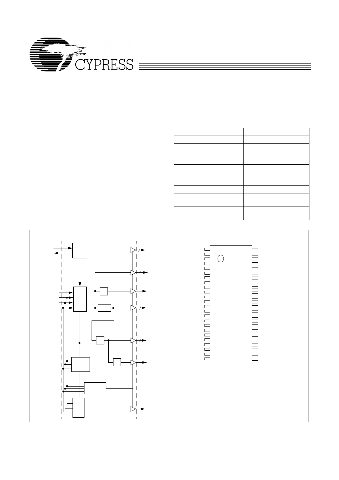
Block Diagram
Pin Configuration
REF_[0:1]
CPU_[0:2]
CPUdiv2
3V66_[0:2]
XTAL
PLL 1
SPREAD#
X2
X1
PCI_[0:9]
IOAPIC
48MHz
PLL2
OSC
÷2
Power
Three-state
Logic
SEL0
SEL1
SEL133/100#
÷2/÷1.5
Down
Logic
÷2
÷2
2
3
3
9
PWRDWN#
REF0
REF1
VDDQ3
X1
X2
GND
PCI0
PCI1
VDDQ3
PCI2
PCI3
PCI4
PCI5
GND
PCI6
PCI7
VDDQ3
PCI8
PCI9
GND
3V66_0
3V66_1
3V66_2
VDDQ3
W161
GND
VDDQ2
IOAPIC
GND
VDDQ2
CPUdiv2
GND
VDDQ2
CPU2
GND
VDDQ2
CPU1
CPU0
GND
VDDQ3
GND
PWRDWN#*
SPREAD#*
SEL1*
SEL0*
VDDQ3
48MHz
GND
SEL133/100#
48
47
46
45
44
43
42
41
40
39
38
37
36
35
34
33
32
31
30
29
28
27
26
25
1
2
3
4
5
6
7
8
9
10
11
12
13
14
15
16
17
18
19
20
21
22
23
24
Note:
1. Internal 250-kΩ pull-up resistors present on inputs marked with *.
Design should not rely solely on internal pull-up resistor to set I/O
pins HIGH.
[1]
Page 2
W161
PRELIMINARY
2
Overview
The W161, a motherboard clock synthesizer, provides 2.5V
CPU clock outputs for advanced CPU and a CPU-divide-by-2
refere nce frequency for Di rect Rambus
Clock Generat or (such
Cypress W134) int erfa ce. Fix ed output f requencie s are provi ded for other system functions.
CPU Frequency Selection
CPU frequency is selected with input pins 25, 29, and 30
(SEL133/100#, SEL0, and SEL1, re specti vel y). Ref er to Table
1 for detail s.
Output Buffer Configuration
Clock Output s
All clock outputs are designed to drive serial terminated clock
lines. The W161 outputs are CMOS-type, which provide
rail-to-rail output swi ng.
Crystal Oscillator
The W161 requires one input ref erence cl oc k to synt hesiz e all
output frequencies. The reference clock can be either an externally generated clock signal or the clock generated by the
internal crystal oscil lator. When using an e x ternal clo c k sig nal,
pin X1 is used as the clock in put and pin X2 is left open.
The internal crystal oscillator is used in conjunction with a
quartz crystal connected t o de vi ce pins X 1 and X2 . Th is f orms
a parallel resonant crystal oscillator circuit. The W161 incorporates the necessary feedback resistor and crystal load capacitors. Including typical stray circuit capacitance, the total
load presented to the crystal is approximately 18 pF. For optimum frequency accuracy without the addition of external capacitors, a parallel-resonant mode crystal s pecifying a load o f
18 pF sh ould be used . This will t ypically y ield referenc e frequency accuracies within ±100 ppm.
Pin Definitions
Pin Name
Pin
No.
Pin
T ype Pin Description
CPU0:2 36, 37, 40 O
CPU Clock Outputs 0 through 2:
CPU clock outputs. Their output volt age
swing is cont rolled by voltag e applied to VDDQ2.
PCI0:9 7, 8, 10, 11, 12,
13, 15, 16, 18,
19
O
PCI Clock Out puts 0 t hrough 9:
Output vo ltage s wing is control led by vo ltage
applied to VDDQ3.
CPUdiv2 43 O
CPU-Divide-By-2 Output:
This serves as a reference input signal for Direct
Rambus Clock G enerator (Cypress W134). The output voltage is determined
by VDDQ2.
3V66_0:2 21, 22, 23 O
66-MHz Clock Outputs 0 through 2:
Output volt age swing is controll ed by
voltage applied to VDDQ3.
IOAPIC 46 O
I/O APIC Clock Output:
Provides an out put synchronous to CPU clock. See
Ta ble 1 for their relation to other system clock outputs.
48 MHz 27 O
48-MHz Output:
Fixed clock output at 48 MHz.
SPREAD# 31 I
Spread Spectrum Enable:
This input enab les spread spectrum modulat ion
on the PLL1 generated f requency outputs of the W161. Modulation range is
–0.5%.
PWRDWN# 32 I
Power Down Control
REF0:1 1, 2 I
Fixed 14.318-MHz Output 0 and 1:
Output volt age swing is controll ed by
voltage applied to VDDQ3.
SEL0:1 29, 30 I
Mode Select Input 0 through 1:
3.3V LVTTL-compatible input for selecting
clock output mo des. As shown in Ta ble 1.
SEL133/100# 25 I
Frequency Selection Input:
3.3V LVTTL-compatible input that selec ts CPU
output frequen cy as shown in Table 1.
X1 4 I
Crystal Connection or Ext ernal Reference Freque ncy Input:
This pin has
dual functions. It can be used as an ex ternal 14.318-MHz crystal connection
or as an external reference frequency input.
X2 5 I
Crystal Connecti on:
An input connec tion f or an e xternal 14.3 18-MHz crystal.
If using an external reference , this pin must be left unconn ected.
VDDQ2 38, 41, 44, 47 P
Power Connection:
Connected to 2.5V power supply.
VDDQ3 3, 9, 17, 24, 28,
34
P
Power Connection:
Connected to 3.3V power supply.
GND 6, 14, 20, 26,
33, 35, 39, 42,
45, 48
G
Ground Connectio n:
Connect all ground pin s to th e common s ystem gr oun d
plane.
Page 3
W161
PRELIMINARY
3
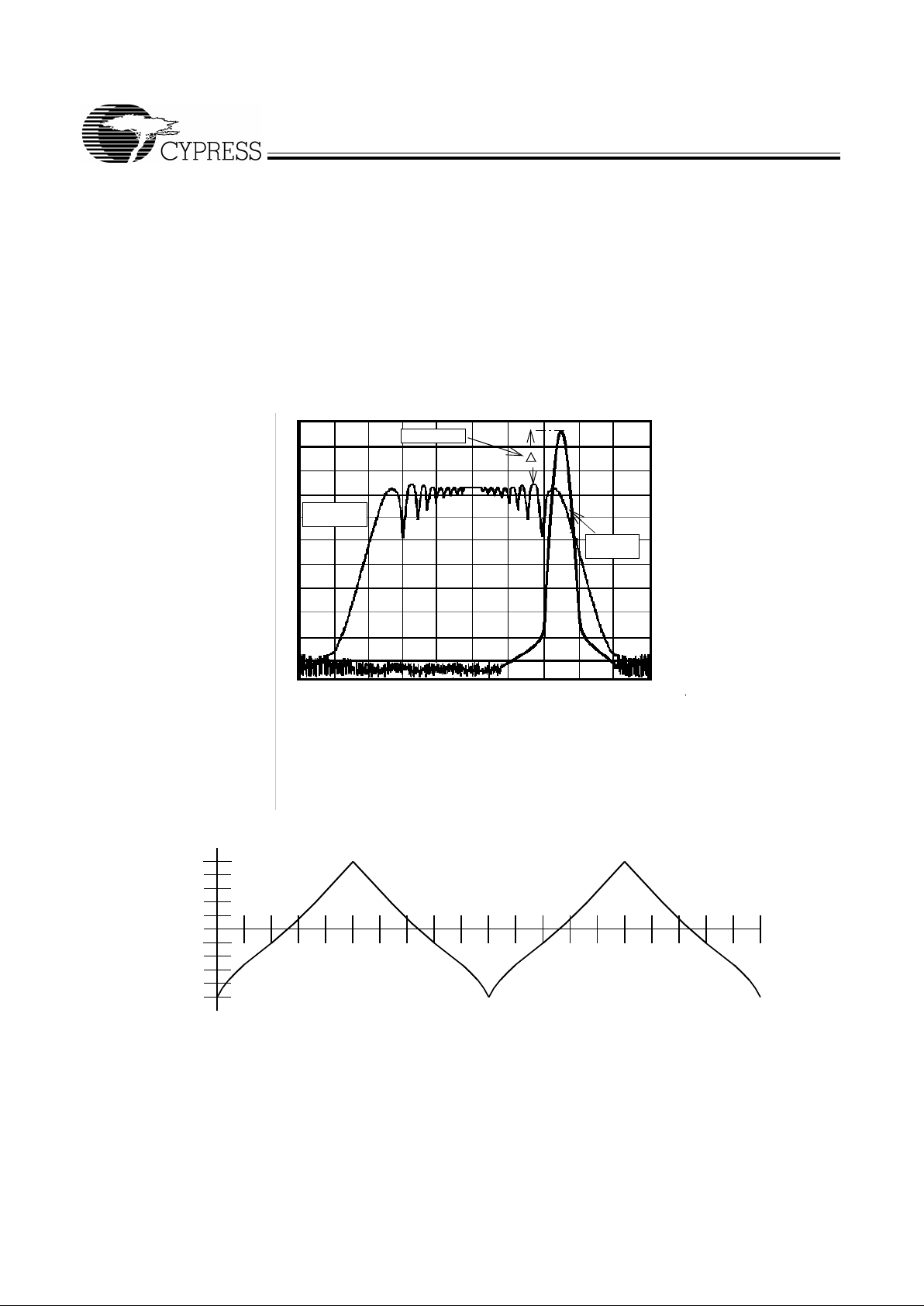
Spread Sp ectrum Feat u re
The device generates a clock that is frequency modulated in
order to increase the bandwidth that it occu pies. By increas ing
the bandwidth of the fundamental and its harmonics, the amplitudes of the radiated electromagnetic emissions are reduced. This effect is depicted in Figure 1.
As shown in Figure 1, a harmonic of a modulated cl ock has a
much low er amplitude th an that of an un modulated si gnal. The
reduction in amplitude is dependent on the harmonic number
and the frequency deviation or spread. The equation for the
reduction is
dB = 6.5 + 9*log
10
(P) + 9*log10(F)
Where P is the perce nta ge of de viati on and F is the frequen cy
in MHz where the reduction is measured.
The output clock is modulated with a waveform depicted in
Figure 2. This waveform, as discussed in “Spread Spect rum
Clock Generation f or the Reducti on of Radiated Emissio ns” by
Bush, Fessler, and Hardin produces the maximum reduction
in the amplitude of radiated electromagnetic emissions. The
deviati on selec ted for this chip i s –0.5% do wnspr ead. Fi gure 2
details the Cypress spr eading pat tern. Cypress does offer options with more spread and greater EMI reduction. Cont act
your local Sales representative for details on these devices .
Spread
Spectrum
Enabled
EMI Reduction
Spread
Spectrum
Non-
Figure 1. Typi cal Clock and SSFTG Comparison
100%
60%
20%
80%
40%
0%
–20%
–40%
–60%
–80%
–100%
10%
20%
30%
40%
50%
60%
70%
80%
90%
100%
10%
20%
30%
40%
50%
60%
70%
80%
90%
100%
Time
Frequency Shift
Figure 2. Typica l Modulation Profile
Page 4

W161
PRELIMINARY
4
Absolute Maximum Ratings
Stresses gre ater th an those list ed i n this tab le may cause permanent damage to the de vice. These represent a str ess ratin g
only. Operation of the device at these or any other conditions
above those specified in the operatin g sections of this specification is not implied. Maximum conditions for extended periods may affect reliability.
.
Parameter Description Rating Unit
V
DD
, V
IN
V oltage on any pin with respect to GND –0.5 to +7 .0 V
T
STG
Storage Temperature –65 to +150 °C
T
A
Operating Temperature 0 to +70 °C
T
B
Ambient Temperature under Bias –55 to +125 °C
ESD
PROT
Input ESD Protection 2 (min.) kV
DC Electr i cal C h ar acteristics :
TA = 0°C to +70°C, V
DDQ3
= 3.3V±5%, V
DDQ2
= 2.5V±5%
Parameter Description Tes t Condi ti on Min. Typ. Max. Unit
Supply Current
I
DD-3.3V
Combined 3.3V Supply Current CPU0:3 =133 MHz
[2]
160 mA
I
DD-2.5
Combined 2.5V Supply Current CPU0:3 =133 MHz
[2]
90 mA
Logic Inputs (All referenced to V
DDQ3
= 3.3V)
V
IL
Input Low V oltage GND –
0.3
0.8 V
V
IH
Input High V oltage 2.0 VDD +
0.3
V
I
IL
Input Low Current
[3]
–25 µA
I
IH
Input High Current
[3]
10 µA
I
IL
Input Low Current, SEL133/100#
[3]
–5µA
I
IH
Input High Current, SEL133/100#
[3]
5µA
Clock Outputs
CPU, CPUdiv2, IO APIC (Referenced to V
DDQ2
) T est Condition Min. Typ. Max. Unit
V
OL
Output Low Voltage IOL = 1 mA 50 mV
V
OH
Output High Voltage IOH = –1 mA 2.2 V
I
OL
Output Low Current V
OL
= 1.25V 45 65 100 mA
I
OH
Output High Current VOH = 1.25V 45 65 100 mA
48MHz, RE F (Refere n ced to V
DDQ3
) Tes t Condi tion Min. Typ. Max. Unit
V
OL
Output Low Voltage IOL = 1 mA 50 mV
V
OH
Output High Voltage I
OH
= –1 mA 3.1 V
I
OL
Output Low Current V
OL
= 1.5V 45 65 100 mA
I
OH
Output High Current V
OH
= 1.5V 45 65 100 mA
PCI, 3V66 (Referenced to V
DDQ3
) Tes t Condi tion Min. Typ. Max. Unit
V
OL
Output Low Voltage I
OL
= 1 mA 50 mV
V
OH
Output High Voltage IOH = –1 mA 3.1 V
I
OL
Output Low Current VOL = 1.5V 70 100 145 mA
I
OH
Output High Current V
OH
= 1.5V 65 95 135 mA
Notes:
2. All clock outputs loaded with 6" 60Ω transmission lines with 20-pF capacitors.
3. W161 logic inputs have internal pull-up devices, except SEL133/100# (pull-ups not CMOS level).
Page 5

W161
PRELIMINARY
5
3.3V AC Electri cal C h ar acteristics
T
A
= 0°C to +70°C, V
DDQ3
= 3.3V±5%,V
DDQ2
= 2.5V± 5%, f
XTL
= 14.31818 MHz
Spread Spectrum functi on turned off
AC clock parameters are tested and guaranteed over stated operating conditions using the stated lump capacitive load at the
clock o utput.
[7]
Notes:
4. X1 input threshold voltage (typical) is V
DD
/2.
5. The W161 contains an internal crystal load capacitor between pin X1 and ground and another between pin X2 and ground. Total load placed on crystal is 18 pF;
this includes typical stray capacitance of short PCB traces to crystal.
6. X1 input capacitance is applicable when driving X1 with an external clock source (X2 is left unconnected).
7. Period, jitter, offset, and skew measured on rising edge at 1.5V.
8. 3V66 is CPU/2 for CPU =133 MHz and (2 x CPU)/3 for CPU = 100 MHz.
Crystal Oscillator
V
TH
X1 Input threshold Voltage
[4]
1.65 V
C
LOAD
Load Capacitance, Imposed on
External C rys tal
[5]
18 pF
C
IN,X1
X1 Input Capacitance
[6]
Pin X2 unconnected 28 pF
Pin Capacitance/Induct ance
C
IN
Input Pin Capacitance Except X1 and X2 5 pF
C
OUT
Output Pin Capacitance 6 pF
L
IN
Input Pin Inductance 7nH
DC Electr i cal C h ar acteristics :
TA = 0°C to +70°C, V
DDQ3
= 3.3V±5%, V
DDQ2
= 2.5V±5% (continued)
Parameter Description Tes t Condi ti on Min. Typ. Max. Unit
3V66 Clock Outputs, 3V66_0:3 (Lump Capacitance Test Load = 30 pF)
Parameter Description Test Condition/Comments Min. Typ . Max. Unit
f Frequency Note 8 66.6 MHz
t
R
Output Rise Edge Rate Measured from 0.4V to 2.4V 1 4 V/ns
t
F
Output Fall Edge Rate Measured from 2.4V to 0.4V 1 4 V/ns
t
D
Duty Cycle Measu red on ris ing and f al ling edge at 1. 5V 45 55 %
f
ST
Frequency Stabilization
from Power-up (cold start)
Assumes full su pply voltage reached within
1 ms from power-up. Short cycles exist prior
to frequency stabilization.
3ms
Z
o
AC Output Impe dance Average value during switching transition.
Used for determining series termination
value.
15 Ω
Page 6

W161
PRELIMINARY
6
Note:
9. PCI clock is CPU/4 for CPU = 133 MHz and CPU/3 for CPU = 100 MHz.
PCI Clock Outputs, PCI0:9 (Lump Capacitance Test Load = 30 pF
Parameter Description Te st Condi tion/Comments Min. Typ. Max. Unit
t
P
Period Measured on rising edge at 1.5V
[9]
30 ns
t
H
High Time Duration of clock cycle above 2.4V 12 ns
t
L
Low Time Duration of clock cycle below 0.4V 12 ns
t
R
Output Rise Edge Rate Measured from 0.4V to 2.4V 1 4 V/ns
t
F
Output Fall Edge Rate Measu red f rom 2.4V to 0.4V 1 4 V/ns
t
D
Duty Cycle Measured on rising and falling edge at 1.5V 45 55 %
t
JC
Jitter , Cycle-to-Cycle Measured on rising edge at 1.5V. Maximum
differ ence of cyc le time be tween tw o adjacent cycles .
500 ps
t
SK
Output Skew Measured on rising edge at 1.5V. 500 ps
t
O
3V66 to PCI Clock Skew Covers all 3V66/PCI outputs. Measured on rising
edge at 1.5V. 3V66 leads PCI output.
1.5 3 ns
f
ST
Frequency Stabilization
from Power-up (cold
start)
Assumes full supply voltage reached within 1 ms
from power-up. Short cycles exist prior to frequency
stabilization.
3ms
Z
o
AC Output Impeda nce Average v alue during switching transition. Used for
determining series termination value.
15 Ω
REF Clock Outputs, REF0:1 (Lump Capaci tance Test Load = 20 pF)
Parameter Description Test Condition/Comments Min. Typ. Max. Unit
f Frequency, Actual Frequency generated by crystal oscillator 14.318
t
R
Output Rise Edge Rate Measured fr om 0.4V t o 2.4V 0.5 2 V/ns
t
F
Output Fall Edge Rate Measured from 2.4V t o 0.4V 0.5 2 V/ns
t
D
Duty Cycle Measured on rising and falling edge at 1.5V 45 55 %
f
ST
Frequency St abilization from
Power-up (cold start)
Assumes full supply voltage reached within
1 ms from power-up. Short cycles exist prior to
frequency stabi li zation.
3ms
Z
o
AC Output Impedance A vera ge value during s witching tran sition. Used
for determining seri es termination value.
25 Ω
48-MHZ Clock Output (Lump Capac it ance Test Load = 20 pF)
Parameter Description Test Condition/Comments Min. Typ. Max. Unit
f Frequency, Actual Determined by PLL divider r atio (see m/n below) 48.008 MHz
f
D
Deviation from 48 MHz (48.008 – 48)/48 +167 ppm
m/n PLL Ratio (14.31818 MHz x 57/17 = 48.008 MHz) 57/17
t
R
Output Rise Edge Rate Measured from 0.4V to 2.4V 0.5 2 V/ns
t
F
Output Fall Edge Rate Measured from 2.4V to 0.4V 0.5 2 V/ns
t
D
Duty Cycle M easured on rising and falling edge at 1.5V 45 55 %
f
ST
Frequency Stabilization
from Power-up (cold start)
Assumes full supply vol tage reached withi n 1 ms
from power-up. Short cycles exist prior to frequency stabilization.
3ms
Z
o
AC Output Impedance Average value during switching transition. Used
for determining seri es termi nation value.
25 Ω
Page 7

W161
PRELIMINARY
7
2.5V AC Electri cal C h ar acteristics
T
A
= 0°C to +70°C, V
DDQ3
= 3.3V±5%, V
DDQ2
= 2.5V±5%
f
XTL
= 14.31818 MHz
Spread Spectrum functi on turned off
AC clock parameters are tested and guaranteed over stated operating conditions using the stated lump capacitive load at the
clock o utput.
[10]
Note:
10. Period, Jitter, offset. and skew measured on rising edge at 1.25V.
CPU Clock Outputs, CPU0:2 (Lump Capacitance Test Load = 20 pF)
Parameter Description Test Condition/Comments
CPU = 133 MHz CPU = 100 MHz
UnitMin. Typ. Max. Min. Typ. Max.
t
P
Period Measured on rising edge at 1.25V 7.5 7.65 10 10.2 ns
t
H
High Time Duration of cl ock cycle above 2.0V 1.87 3. 0 ns
t
L
Low Time Duration of clock cycle below 0.4V 1.67 2.8 ns
t
R
Output Rise Edge Rate Measured from 0.4V to 2.0V 1 4 1 4 V/ns
t
F
Output Fall Edge Rate Measured from 2.0V to 0.4V 1 4 1 4 V/ns
t
D
Duty Cycle Measured on rising and falling edge at
1.25V
45 55 45 55 %
t
JC
Jitter , Cycle-to-Cycle Measured on rising edge at 1.25V. Max-
imum differ ence of cycle time bet w een
two adjacent cycles.
250 250 ps
t
SK
Output Skew Measured on rising edge at 1.25V 175 175 ps
f
ST
Frequency Stabilization from Po wer-up
(cold start)
Assumes full supply voltage reached
within 1 ms from power-up . Short cycles
exist prior to frequency stabilizat ion.
33ms
CPUdiv2 Clock Outputs, CPUdiv 2 (Lump Capacitance Test Load = 20 pF)
Parameter Description Test Condition/Comments
CPU = 133 MHz CPU = 100 MHz
UnitMin. Typ. Max. Min. Typ. Max.
t
P
Period Measured on rising edge at 1.25V 15 15.3 20 20.4 ns
t
H
High Time Duration of clock cycle above 2.0V 5.25 7.5 ns
t
L
Low Time Duration of clock cycle below 0.4V 5.05 7.3 ns
t
R
Output Rise Ed ge Rate Measured from 0.4V to 2.0V 1 4 1 4 V/ns
t
F
Output Fall Edge Rate Measured from 2.0V to 0.4V 1 4 1 4 V/ns
t
D
Duty Cycle Measured on ris ing and falling edge at
1.25V
45 55 45 55 %
t
JC
Jitter , Cycle-to- Cycle Measured on rising edge at 1.25V . Max-
imum difference of cyc le time between
two adjacent cycles.
250 250 ps
t
SK
Output Skew Measured on rising edge at 1.25V 175 175 ps
f
ST
Frequency Stabilization from Po wer-up
(cold start)
Assumes full suppl y voltage reached
within 1 ms from po wer-up. Short cyc les
exist prior to frequency stabilization.
33ms
Z
o
AC Output Impeda nce Average value during switching transi-
tion. Used for det ermining series termination val ue.
20 20 Ω
Page 8

W161
PRELIMINARY
8
Note:
11. IOAPIC clock is CPU/8 for CPU = 133 MHz and CPU/6 for CPU = 100 MHz.
Document #: 38-00817
IOAPIC Clock Output, IOAPIC (L ump Capacit ance Te st Load = 20 pF)
Parameter Description Test Condition/Comments Min Typ Max Unit
f Frequency Note 11 16.67 MHz
t
R
Output Rise Edge Rate Measured from 0.4V to 2.0V 1 4 V/n s
t
F
Output Fal l Edge Rate Measured from 2.0V to 0.4V 1 4 V/ns
t
D
Duty Cycle M easured on rising and falling edge at 1.25V 45 55 %
f
ST
Frequency Stabilization
from Power-up (cold start)
Assumes full supply voltage reached within
1 ms from power-up . Sh ort cycles exist prior to
frequency stabi li zation.
3ms
Z
o
AC Output Impedance Av erage value duri ng switching tran sition. Used
for determining seri es termi nation value.
20 Ω
Ordering Information
Ordering Code
Package
Name Package Type
W161 H 48-pin SSOP (300 mils)
Page 9

W161
PRELIMINARY
© Cypress Semiconductor Corporation, 1999. The information contained herein is subject to change without notice. Cypress Semiconductor Corporation assumes no responsibility for the use
of any circuitry other than circuitry embodied in a Cypress Semiconductor product. Nor does it con vey or imply any license under patent or other rights. Cypress Semiconductor does not authorize
its products for use as critical components in life-support systems where a malfunction or failure may reasonably be expected to result in significant injury to the user. The inclusion of Cypress
Semiconductor products in life-support systems application implies that the manufacturer assumes all risk of such use and in doing so indemnifies Cypress Semiconductor against all charges.
Package Diagram
48-Pin Small Shrink Outlin e P ackage (SSOP, 300 mils)
Summary of nominal dimensions in inches:
Body Width: 0.296
Lead Pitch: 0.025
Body Length: 0.625
Body Height: 0.102
 Loading...