

Page 1
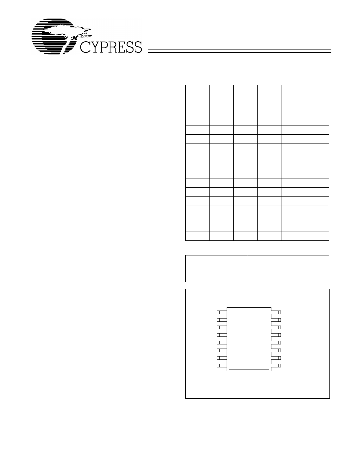
Pin Configuration
TEST
VDD
USBCLK/SS%*
GND
SYSCLK
GND
FS0*
SSON#^
16
15
14
13
12
11
10
9
VDD
X1
X2
GND
FS3*
VDD
FS2*
FS1*
1
2
3
4
5
6
7
8
W155
[1]
Note:
1. Internal pull-up resistor present on inputs marked with ‘*’ and pull-down
resistor present on input marked with ‘^’.
W155
Spread Spectrum Frequency Timing Generator
Features
• Generates a spread spectrum timin g signal (SYSCLK)
and a non-spread signal (USBCL K)
• Requires a 14.318-MHz crystal for oper a ti on
• Supports MIPS microprocessor clock frequencies
• Reduces peak EMI by as much as 12 dB
• Integrated loop filter components
• Cycle-to-cycle jitter = 250 ps (max)
• Operates with a 3.3 or 5.0V power supply
• Spread output is selectable from 10 to 133 MHz
• TEST mode supports modulation off (High-Z ) and special test input reference frequency
• Guaranteed 45/55 duty cycle
• Pack aged in a 16-pin, 300-mil -wide SOIC (Small Outli ne
Integrated Circuit)
Overview
The W155 incorporates the latest advances in PLL-based
spread spectrum frequency synthesizer technology. By frequency modulating the SYSCLK output with a low-frequency
carrier, peak EMI can be great ly reduced in a system. Use of
this technique all ows systems to pass inc reasingly difficu lt EMI
testing without resorting to costly shielding or redesi gn.
In a system that uses t he W155, not only is EMI reduce d in the
various clock lines, but also in all signals which are synchronized to SYSCLK. Therefore, the benefits of using this technique increase with the number of address and data lines in
the system.
The W1 55 is spe cif ically tar get ed towa rd MI PS micr opr oces sor based systems where EMI is of particular concern. Each
device uses a single 14. 318- MHz crystal to gen erate a selectable spread spectrum output and an unmodulated 48-MHz
USB Output.
The spreading func ti on can be disabled b y taking the SSON#
pin high. Spread percent age can be selected with the SS%
input (see
Table 2
below ).
Table 1. Frequency Selection (14.318-MHz Reference)
SYSCLK
FS3 FS2 FS1 FS0
(Output Freq.)
0000133.3 MHz
0001 120 MHz
0010 100 MHz
001174.77 MHz
0100 70 MHz
0101 66.6 MHz
0110 60 MHz
0111 50 MHz
1000 40 MHz
100133.33 MHz
1010 30 MHz
1011 25 MHz
1100 20 MHz
110116.67 MHz
1110 12 MHz
1111 10 MHz
T able 2. Spread Per centage Selection
SS% Spread Percentage
0 –1.25%
1 –3.75%
Cypress Semiconductor Corporation
• 3901 North First Street • San Jose • CA 95134 • 408-943-2600
September 29, 1999, r ev. **
Page 2
Pin Definitions
Pin Name Pin No. Pin Type Pin Description
USBCLK/
SS%
SYSCLK 12 O
FS0:3 10, 8, 7, 5 I
SSON# 9 I
X1 2 I
X2 3 I
TEST 16 I
VDD 1, 6, 15 P
GND 4, 11, 13 G
14 I/O
USB Clock Output /Modulation Width Se lection Input:
spectrum feature is enabled, this pin is used to select the amount of frequency
variation on the SYSCLK out put (see Ta bl e 2). Wider variations result in greater
peak EMI reduction. When an output: supplies a non-spread 48-MHz signal for
USB support.
System Clock Output :
ture is controlled by pins 9 & 14.
Frequency Select Pi ns:
the SYSCLK output.
Spread Spectrum Contr ol (active LO W):
internal modulati ng wavefor m off. This pin has an internal pull-down resistor.
Crystal Connection or Exter nal Reference Frequenc y Input:
functions . It can be used as either an e xternal crystal connecti on, or as an ex ternal
reference frequency input.
Crystal Connection:
nected.
Te st Mode:
Power Connection:
must be the same voltage level.
Ground Connection:
For normal operation, tie this pin to ground.
Freq uency is se lecte d per Table 1. Spread spectrum fea -
These pins set the frequency of the signal pro vided at
If using an external reference, this pin must be left uncon-
Connected to either 3.3V or 5.0V power supply . All VDD pins
Connect to t he common system ground plane.
W155
When an input; if spread
Pulling this i nput signal HIGH turns the
This pin has du al
2
Page 3

W155
Functional Description
I/O Pin Operation
Pin 14 is a dual purpose l/O pin.
Upon power-up eac h I/O pin acts as a logi c input, allo wing th e
determination of assigned device functions . A short time after
power-up, the logic state of each pin is latched and each pin
then becomes a clock output. This feature reduces device pin
count by combining clock outputs with input select pi ns.
An external 10-kΩ “strapping” resistor is connected between
each l/O pin and ground or V
“0” bit, connection to V
DD
Upon W155 power -up, the first 2 ms of operation is used for
input log ic selec tion. During this period, each clock output b uffer is three-stated, allowing the output strapping resistor on
each l/O pin to pull the pin and its associated capaciti ve clock
load to either a logic HIGH or LOW state. At the end of the
2-ms period, the established logic 0 or 1 conditi on of each l/O
pin is then latched . Next the output b uffer is ena bled conv erting
all l/O pins into operating clock outputs. The 2-ms timer starts
when V
turni ng V
reaches 2.0V. The input bits can only be reset by
DD
off and then back on again.
DD
It should be noted that the strapping resistors have no significant effect on clock output signal integrity. The drive impedance of the clock out puts is <40Ω (nominal) which i s m inimal ly
affected by the 10-kΩ strap to ground or V
ries termination resistor, the output strapping resi stor should
be placed as close to the l/O pin as possible in order to keep
the interconnecting trace short. The trace from the resistor to
ground or V
prevent system noise coupling during input log ic sampling.
should be k ept less than t wo inches in length to
DD
When each clock output is enabled following the 2-ms input
period, target (normal) out put freque ncy is del ivere d assuming
. Connection to ground sets a
DD
sets a “1” bit. Se e Figure 1.
. As wi th th e s e -
DD
that V
has stabilized. If VDD has not yet reached full value,
DD
output frequenc y initi ally ma y be below t arget b ut will in crease
to target once V
short output clock cycle may be produced from the CPU clock
voltage has stabilized. In either case, a
DD
outputs when the outputs are enabled.
Output Buffer Configurati on
Clock Outputs
All clock outputs are designed t o driv e serial terminated clock
lines. The device outputs are CMOS-type which provide
rail-to-r ail output swing.
Crystal Oscillator
The device requi res one input refere nce clock t o synthesiz e all
output frequencies. The reference clock can be either an externally generated clock signal or the clock generat ed by the
internal crystal oscil lator. When using an e x ternal c loc k s ignal ,
pin X1 is used as the clock input and pin X2 is left open. The
input threshold voltage of pin X1 is (V
DD
)/2.
The internal crystal oscillator is used in conjunction with a
quartz crystal connected t o de vi ce pins X 1 and X2 . Th is f orms
a parallel resonant crystal oscillator circuit. The device incorporates the necessary feedback resistor and crystal load capacitors. Including typical stray circuit capacitance, the total
load presented to the crystal is approximately 20 pF. For optimum frequency accuracy without the addition of exter nal capacitors, a parallel-r esonant mode crystal specifying a load of
20 pF sh ould be use d. This will t ypically y ield referenc e frequency accuraci es within ±100 ppm. To achieve similar accuracies with a crystal calling for a greater load, external capacitors must be added such t hat the to tal l oad (in ternal, e xt ernal,
and parasitic capacitors) equals t hat called for by the crystal.
W155
Power-on
Reset
Timer
Output
Buffer
Output Three-state
Figure 1. Input Logic Selection Through Jumper Opti on
Hold
Output
Low
QD
Data
Latch
Jumper Options
10 k
Ω
V
DD
Output Strapping Resistor
Series Termination Resistor
R
Clock Load
3
Page 4

W155
Spread Spectrum Frequency Tim ing G enera to r
The device gener ates a clock that is frequency modulated in
order to increase the bandwidth that it occu pies. By increas ing
the bandwidth of the fundamental and its harmonics, the amplitudes of the radiated electromagnetic emissions are reduced. This effect is depicted in Figure 2.
As shown in Figure 2, a harmonic of a modulated clock has a
much low er amplitu de than that of an un modulated si gnal. The
reduction in amplitude is dependent on the harmonic number
and the frequency deviation or spread. The equation for the
reduction is
dB = 6.5 + 9*log
(P) + 9*log10(F)
10
Spread
Spectrum
Enabled
EMI Reduction
Where P is the percenta ge of de vi ation and F is the frequen cy
in MHz where the reduction is measured.
The output clock is modulated with a waveform depicted in
Figure 3. This waveform , as discussed in “Spread Spectrum
Clock Generation f or the Reducti on of Radiated Emissio ns” by
Bush, Fessler, and Hardin produces the maximum reduction
in the amplitude of radiated electromagnetic emissions. The
deviati on select ed for this chi p is speci fied in Table 2. Figure 3
details the Cypress spr eading pat tern. Cypres s does off er options with more spread and greater EMI reduction. Contact
your local sales representative for detai ls on these devices.
Spread Spectrum clocking is activated or deactivated by selecting the appropri ate values f or pin 9.
Non-
Spread
Spectrum
Figure 2. Clock Harmonic with and without SSCG Modulation Frequency Domain Representation
MAX
10%
20%
30%
40%
50%
60%
70%
80%
FREQUENCY
MIN
90%
100%
10%
20%
30%
40%
50%
60%
70%
80%
Figure 3. Typical Modulation Pr ofile
4
90%
100%
Page 5

Absolute Maximum Ratings
W155
Stresses gre ater th an those li sted i n this tab le may cause permanent damage to the de vice. These represent a stress ratin g
only. Operation of the device at these or any other conditions
.
above those specified in the operating sections of this specification is not implied. Maximum conditions for extended periods may affect reliability
Parameter Description Rating Unit
V
, V
DD
IN
T
STG
T
A
T
B
DC Electr i cal C h ar acteristi cs:
Voltage on any pin with respect to GND –0.5 to +7 .0 V
Storage Temperature –65 to +150 °C
Operating Temperatu re 0 to +70 °C
Ambient Temperature under Bias –55 to +125 °C
0°C < TA < 70°C, VDD = 3.30V±10%
Paramet er Description T est Condition Min Typ Max Unit
I
V
V
V
V
I
I
I
I
C
C
DD
IL
IH
OL
OH
OL
OH
IL
IH
I
L
Supply Current 35 mA
Input Low Voltage 0.8 V
Input High Voltage 2.0 V
Output Low Voltage IOL = 2 mA 50 mV
Output High Voltage IOH = –2 mA 3.10 V
Output Low Curren t VOL = 1.5V 80 110 155 mA
Output High Current VOH = 1.5V 80 120 175 mA
Input Low Current 10 µA
Input High Current 10 µA
Input Capacitance 5 10 pF
XTAL Load Capacitance 20 pF
Switching Characteristics
Parameter Description Test Condi tions Min Typ Max Unit
, t
t
TLH
THL
t
TLH, tTHL
t
SYM
t
JCC
Output Rise and F all Time measured
at 10% of 90% of V
DD
Output Rise and F all Time measured
0.8 4.0 ns
0.3 1.0 ns
at 0.8V–2.0V
Output D u ty Cycle 45 55 %
Cycle-to-Cycle Jitter 250 ps
EMI EMI Attenuation 11th Harmonic, 25 MHz 10 dB
Ordering Information
Ordering Code
W155 G 16-pin Plastic SOIC (300 -mil, wide body)
Document #: 38- 00785
Package
Name Package Type
5
Page 6

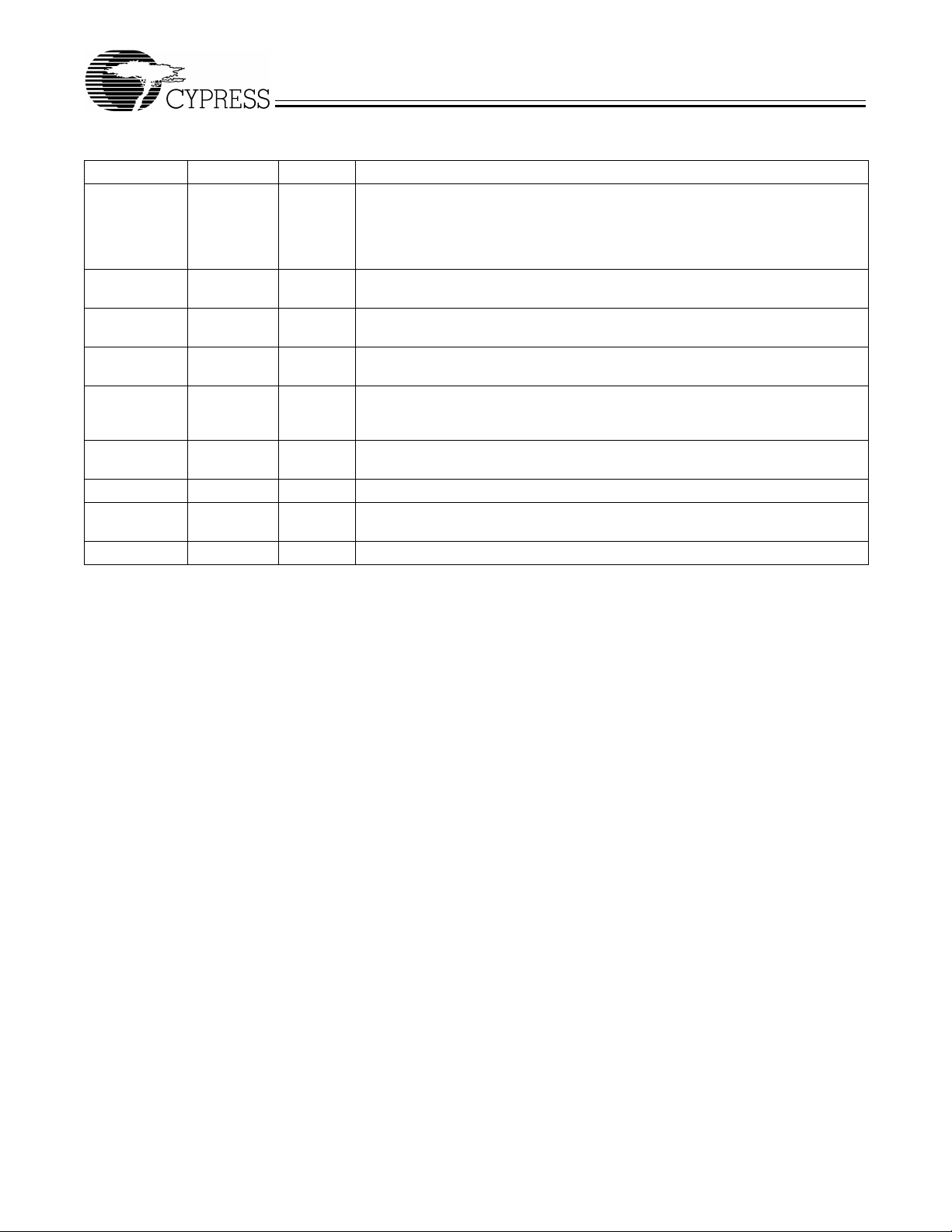
Package Diagram
W155
16-Pin Small Outlined Integrated Circuit (SOIC, 300 mils, wide body)
1
8
0.285 – 0.299
(7.42 – 7.59)
0.40 – 0.41
(10.16 – 10.41)
All linear dimensions are in inches and parent he tic ally in millimeters, min. – max.
Note:
16
0.009 - 0.0125
0.399 - 0.412
(10.13 - 10.46)
9
0.014 - 0.019
(0.35 - 0.48)
(0.23 - 0.32)
0.189 - 0.196
(4.80 - 4.98)
0.024 - 0.040
(0.61 - 1.02)
0.05 (1. 27)
BSC
5°Nom
0.097 - 0.104
(2.46 - 2.64)
0.0020 – 0.015
(0.06 – 0.3 8)
© Cypress Semiconductor Corporation, 1999. The information contained herein is subject to change without notice. Cypress Semiconductor Corporation assumes no responsibility for the use
of any circuitry other than circuitry embodied in a Cypress Semiconductor product. Nor does it con vey or imply any lice nse under patent or other rights. Cypress Semicondu ctor does not authorize
its products for use as critical components in life-support systems where a malfunction or failure may reasonably be expected to result in significant injury to the user. The inclusion of Cypress
Semiconductor products in life-support systems application implies that the manufacturer assumes all risk of such use and in doing so indemnifies Cypress Semiconductor against all charges.
 Loading...