

Page 1
PRELIMINARY
440BX AGPset Spread Spectrum Frequency Synthesizer
Features
• Maximized EMI suppression usi ng Cypress’s Spread
Spectrum Technology
• Single chip system frequency synthesizer for Intel
440BX AGPset
• Three copies of CPU output
• Seven copies of PCI output
• One 48-MHz output for USB / One 24-MHz for SIO
• T wo buffered reference outputs
• Two IOAPIC outputs
• 17 SDRAM outputs provide support for 4 DIMMs
• Supports frequencies up to 150 MHz
2
•I
C™ interface for programming
• Power man agement control inputs
Key Specific ati o n s
CPU Cycle-to-Cycle Jitter: ........... ........... .. ................. 250 ps
CPU to CPU Output Skew: ............... ................. ........ 175 ps
PCI to PCI Output Skew:........................... .. .. .............500 ps
SDRAM IN to SDRAM0 :1 5 Delay : ..... ... ................. .3 .7 ns typ.
: .................................................................... 3.3V±5%
V
DDQ3
: .................................................................... 2.5V±5%
V
DDQ2
SDRAM0:15 (leads) to SDRAM_F Skew:..............0.4 ns typ.
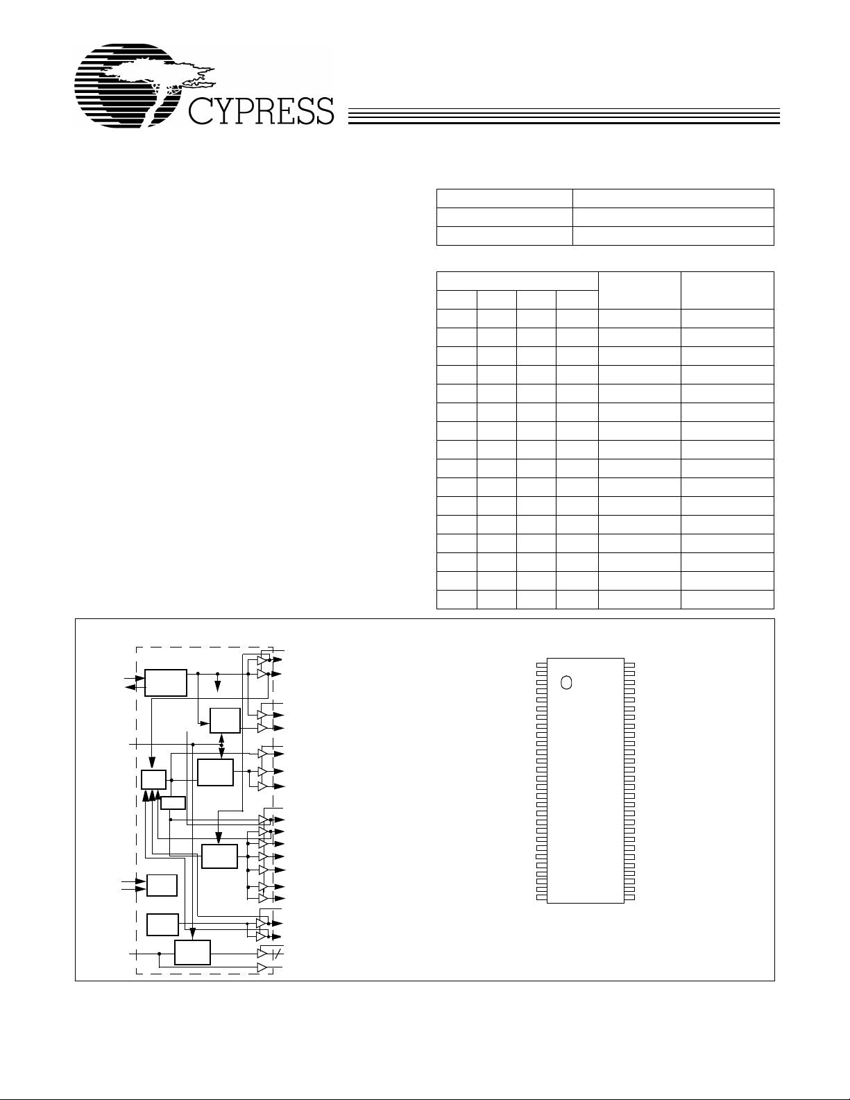
Logic Block Diagram
VDDQ3
REF0/(PCI_STOP#)
X1
X2
CLK_STOP#
SDATA
SCLK
SDRAMIN
PLL 1
Logic
PLL2
XTAL
OSC
÷2,3,4
I2C
I/O Pin
Control
PLL Ref Freq
Stop
Clock
Control
Stop
Clock
Control
Stop
Clock
Control
Stop
Clock
Control
REF1/FS2
VDDQ2
IOAPIC_F
IOAPIC0
VDDQ2
CPU_F
CPU1
CPU2
VDDQ3
PCI_F/MODE
PCI0/FS3
PCI1
PCI2
PCI3
PCI4
PCI5
VDDQ3
48MHz/FS1
24MHz/FS0
VDDQ3
SDRAM0:15
16
SDRAM_F
®
T able 1. Mode Input Table
Mode Pin 3
0PCI_STOP#
1REF0
T able 2. Pin Selectable Frequency
Input Address
CPU_F, 1:2
(MHz)
PCI_F, 0:5
(MHz)FS3 FS2 FS1 FS0
1 1 1 1 133.3 33.3 (CPU/4)
1 1 1 0 124 31 (CPU/4)
1 1 0 1 150 37.5 (CPU/4)
1 1 0 0 140 35 (CPU/4)
1 0 1 1 105 35 (CPU/3)
1 0 1 0 110 36.7 (CPU/3)
1 0 0 1 115 38.3 (CPU/3)
1 0 0 0 120 40 (CPU/3)
0 1 1 1 100 33.3 (CPU/3)
0 1 1 0 133.3 44.43 (CPU/ 3)
0 1 0 1 112 37.3 (CPU/3)
0 1 0 0 103 34.3 (CPU/3)
0 0 1 1 66.8 33.4 (CPU/2)
0 0 1 0 83.3 41.7 (CPU/2)
0 0 0 1 75 37.5 (CPU/2)
0 0 0 0 124 41.3 (CPU/3)
Pin Configuration
VDDQ3
REF1/FS2
REF0/(PCI_STOP#)
GND
VDDQ3
PCI_F/MODE
PCI0/FS3
GND
PCI1
PCI2
PCI3
PCI4
VDDQ3
PCI5
SDRAMIN
SDRAM11
SDRAM10
VDDQ3
SDRAM9
SDRAM8
GND
SDRAM15
SDRAM14
GND
SDATA
SCLK
[1]
VDDQ2
W150
56
55
54
53
52
51
50
49
48
47
46
45
44
43
42
41
40
39
38
37
36
35
34
33
32
31
30
29
IOAPIC0
IOAPIC_F
GND
CPU_F
CPU1
VDDQ2
CPU2
GND
CLK_STOP#
SDRAM_F
VDDQ3
SDRAM0
SDRAM1
GND
SDRAM2
SDRAM3
SDRAM4
SDRAM5
VDDQ3
SDRAM6
SDRAM7
GND
SDRAM12
SDRAM13
VDDQ3
24MHz/FS0
48MHz/FS1
1
2
3
4
X1
5
X2
6
7
8
9
10
11
12
13
14
15
16
17
18
19
20
21
22
23
24
25
26
27
28
W150
Intel is a registered trademark of Intel Corporation. I2C is a trademark of Philips Corporation.
Note:
1. Internal pull-up resistors should not be relied upon for setting I/O pins HIGH. Pin function with parentheses determined by MODE pin resistor strapping.
Unlike other I/O pins, input FS3 has an internal pull-down resistor.
Cypress Semiconductor Corporation
• 3901 North First Street • San Jose • CA 95134 • 408-943-2600
February 10, 2000, re v. *A
Page 2
PRELIMINARY
Pin Definitions
Pin Name Pin No.
CPU1:2 51, 49 O
CPU_F 52 O
PCI1:5 11, 12, 13 , 14, 16O
PCI0/FS3 9 I/O
PCI_F/MODE 8 I/O
CLK_STOP# 47 I
IOAPIC_F 54 O
IOAPIC0 55 I/O
48MHz/FS1 29 I/O
24MHz/FS0 30 I/O
REF1/FS2 2 I/O
REF0
(PCI_STOP#)
SDRAMIN 17 I
SDRAM0:15 44, 43 , 41, 40,
SDRAM_F 46 O
SCLK 28 I Clock pin f or I
SDATA 27 I/O Data pin for I
X1 5 I
X2 6 I
VDDQ3 1, 7, 15, 20,
3I/O
39, 38, 36, 35 ,
22, 21, 19, 18 ,
33, 32, 25, 24
31, 37, 45
Pin
T ype Pin Description
CPU Outputs 1 and 2:
interface, see Tables 2 and 6. These outputs are affected by the CLK_STOP# input.
Free-Running CPU Output:
input inte rface , see Tables 2 and 6. This output is not aff ected by the CLK_ST OP# input.
PCI Outputs 1 through 5:
interface, see Tables 2 and 6. These outputs are affected by the PCI_STOP# input.
PCI Output/Frequenc y Select Input:
inputs or through serial input interface, see Tables 2 and 6. This output is affected by
the PCI_STOP # input. When an inpu t, latche s data selecti ng the frequen cy of the CPU
and PCI outputs.
Free Running PCI Output:
interf ace, see Tables 2 and 6. This output is not affe cted by th e PCI_STOP# input. When
an input, selects function of pin 3 as described in Tabl e 1 .
CLK_STOP# Input:
pleting a full clock cycle (2–3 CPU clock laten cy). When brought HI GH, affected out puts
start beginning with a full clock cycle (2–3 CPU clock latency).
Free-running IO API C Output:
which is not aff ected b y the CPU_ST OP# logi c input. It’s swi ng is set by vol tage applied
to VDDQ2.
IOAPIC Out put:
by voltag e applied to VDDQ2. This output is disabled when CLK_STOP# is set LOW.
48-MHz Output:
output can be used as the ref ere nce f or the Univ e rsal Serial Bus. Upon po wer up , FS1
input will be latched, setting output frequ encies as described in Table 2.
24-MHz Output:
output can be used as the clock input for a Super I/O chip. Upon power up, FS0 input
will be latched, setting output frequencies as described in Table 2.
Reference Output:
input will be latched, setting output frequ encies as described in Table 2.
Fixed 14.318-MHz Outp ut 0 or PCI_ST OP # Pin:
The PCI_STOP# input enables the PCI 0:5 output s when HIGH and causes them to
remain at logic 0 when LO W. The PCI_STOP signal is latched on the rising edge of
PCI_F. Its effects ta ke place on the next PCI_ F cloc k cycle. As an output , this pin
provides a fix ed cl ock si gna l equal i n frequen cy to the r efe renc e signal provi ded at the
X1/X2 pins (14.318 MHz).
Buffered Input Pin:
(SDRAM0:15, SDRAM_F).
Buffered Outputs:
O
vided at the SDRAMIN input. The sw ing is set by VDDQ3, and they are deactivated
when CLK_STOP# inpu t i s set LOW .
Free-Running Buffered Out put:
input. The swing is set by VDDQ3; this signal is unaffected by the CLK_STOP# input.
Crystal Connection or External Reference Fr equency Input:
tions. It can be used as an external 14.318MHz crystal connection or as an external
reference frequency input.
Crystal Connection:
an external reference, this pin must be left unconnecte d.
Power Connecti on:
P
PCI output buffers, referenc e output buffers, and 48-MHz/24-MHz output buffers. Connect to 3.3V.
Frequen cy is set by the FS0:3 inputs or through serial input
Frequency is set by the FS0:3 inputs or through serial
Frequen cy is set by the FS0:3 inputs or t hrough serial input
As an output, frequency is set by the FS0:3
Fr equency is set by the FS0: 3 inputs or through seri al input
When brought LO W , aff ected o utputs are stopped L OW after c om-
This output is a b uf fer ed v ersi on of th e ref erence inp ut
Provides 14.318-MHz fix ed frequenc y . The output volt age sw ing is set
48 MHz is provided in normal operation. In standard systems, this
24 MHz is provided in normal operation. In standard systems, this
14.318 MHz is provi ded in normal operatio n. Upon power-u p, FS2
Function determined by MODE pin.
The signal provided to this input pin is buffered to 17 outputs
These sixteen dedicated outputs provide copies of the signal pro-
This output provi des a singl e co py of the SDRAMIN
2
C circuitry .
2
C circuitry.
This pin has dual func -
An input connec tion f or an e xternal 14.318- MHz crystal . If using
Pow er supply f or core logic, PLL circui try , SDRAM output buff ers ,
W150
2
Page 3
PRELIMINARY
W150
Pin Definitions
(continued)
Pin
Pin Name Pin No.
VDDQ2 50, 56 P
T ype Pin Description
Power Connecti on:
or 3.3V.
GND 4, 10, 23, 26,
Ground Connections:
G
34, 42, 48, 53
Overview
The W150 was designed as a single-chip alternative to the
standard two-chip Intel 440BX AGPset clock solution. It provides sufficient outputs to support most single-processor, four
SDRAM DIMM designs.
Functional Description
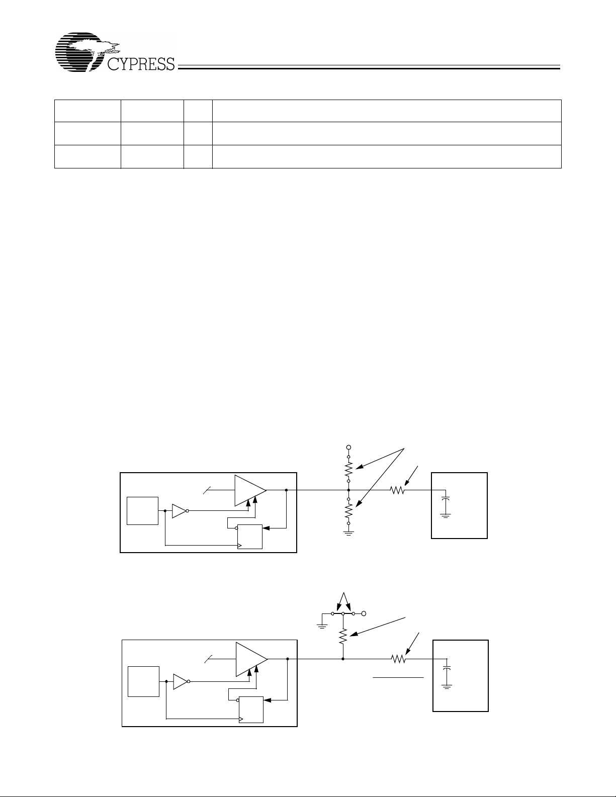
I/O Pin Operation
Pins 2, 8, 9, 29, and 30 are dual-purpose l/O pins. Upon
power-up these pins act as logic inputs, allowing the determination of assigned device functions. A short time after
power-up, the logic state of each pin is latched and the pins
become clock outputs. This feature reduces device pin count
by combining clock outputs with input select pins.
An external 10-kΩ “strapping” resistor is connected between
the l/O pin and ground or V
latch to “0,” connection to V
Figure 2 show two suggested methods for strapping resistor
connections.
Upon W150 power-up, the first 2 ms of operation is used for
input logic selection. During t his period, the five I/O pins (2, 8,
9, 29, 30) are three- stated, all owing the out put strappi ng resis-
. Connection to ground sets a
DD
sets a latch to “1.” Fig ure 1 an d
DD
Pow er supply for IOAPIC and CPU output buff ers. Connect to 2.5V
Connect all groun d pins to the common system ground plane.
tor on the l/O pins to pull the pins and their associated capacitive cloc k load to either a logi c HIGH or LO W st at e. At the end
of the 2-ms peri od, the establ ished logic “0” or “1” condition of
the l/O pin is latched. Next the output buffer is enabled, converting the l/O pin s int o opera ting clo ck ou tpu ts. The 2-ms ti mer starts when V
reset b y turning V
reaches 2.0V. The input bits can only be
DD
off and then back on again.
DD
It should be noted that the strapping resistors have no significant effect on clock output signal integrity. The drive impedance of clock output (<40Ω, nominal) is minimally affected by
the 10-kΩ strap to ground or V
tion resistor, the output strap ping resi stor shou ld be placed as
. As with th e se ries termina-
DD
close to the l/O pin as possible in order to keep the interconnecting trace short. The trace from the resistor to ground or
V
should be kept less than two inches in length to minimize
DD
system noise coupli ng during input logic sampli ng.
When the clock outputs are enabled following the 2-ms input
period, the corresponding specified output frequency is delivered on the pins , assu ming t hat V
not yet reached full value, output frequency initially may be
below target but will increase to target once V
stabilized. In either case, a short output clock cycle may be
has stabiliz ed. If VDD has
DD
voltage has
DD
produced from the CPU clock outputs when the outputs are
enabled.
W150
Power-on
Reset
Timer
W150
Power-on
Reset
Timer
V
Output
Buffer
Output Three -state
QD
Data
Latch
Hold
Output
Low
10 k
(Load Option 1)
10 k
(Load Option 0)
DD
Ω
Ω
Output Strapping Resistor
Series Term ination R es istor
Figure 1. Input Logic Selection Through Resistor Load Option
Jumper O pti on s
Output St rapping Resistor
V
DD
Series Termination Resistor
R
Output
Buffer
Output Three-state
QD
Data
Latch
Hold
Output
Low
10 k
Ω
Resistor Value R
Clock Load
Clock Load
Figure 2. Input Logic Selection Through Jumper Opti on
3
Page 4
PRELIMINARY
W150
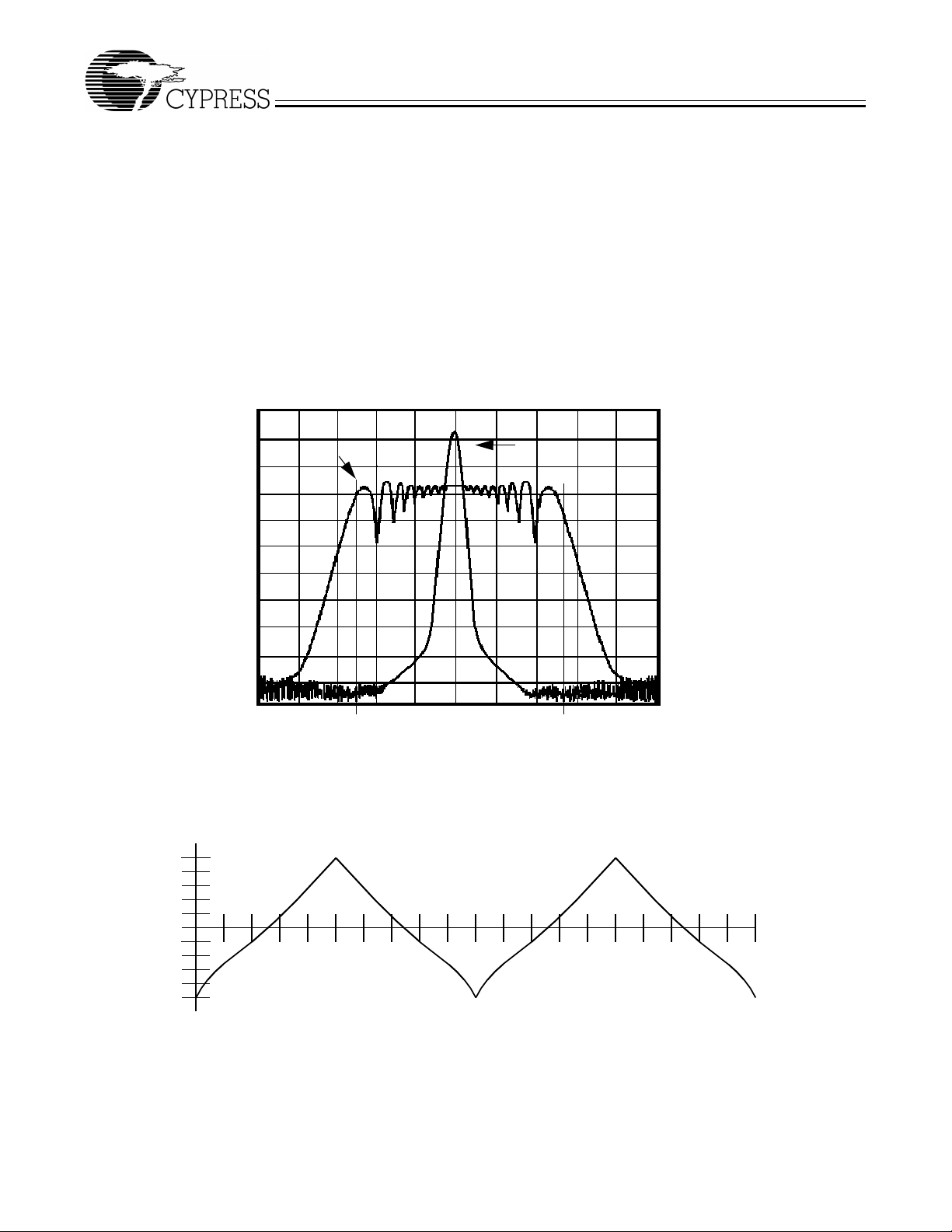
Spread Sp ectrum Generator
The device generates a clock that is frequency modulated in
order to increase the bandwidth that it occu pies. By increas ing
the bandwidth of the fundamental and its harmonics, the amplitudes of the radiated electromagnetic emissions are reduced. This effect is depicted in Figure 3.
As shown in Figure 3, a harmonic of a modulated clock has a
much low er amplitu de than that of an un modulated si gnal. The
reduction in amplitude is dependent on the harmonic number
and the frequency deviation or spread. The equation for the
reduction is
dB = 6.5 + 9*log10(P) + 9*log10(F)
5 dB/d iv
SSFTG Typical Clock
Amplitude (dB)
Where P is the percenta ge of de vi ation and F is the frequen cy
in MHz where the reduction is measured.
The output clock is modulated with a waveform depicted in
Figure 4. This waveform, as discussed in “Spread Spectrum
Clock Generation f or the Reducti on of Radiated Emissio ns” by
Bush, Fessler, and Hardin produces the maximum reduction
in the amplitude of radiated electromagnetic emissions. The
deviati on select ed for this chi p is speci fied in Table 6. Figure 4
details the Cypress spr eading pat tern. Cypres s does off er options with more spread and greater EMI reduction. Contact
your local Sales representative for details on these devices .
Spread Spectrum clocking is activated or deactivated by selecting the appropriate v al ues fo r bits 1–0 in data byte 0 of the
2
I
C data stream. Refer to Table 7 for more deta ils.
–1.0
–0.5%
–SS%
Frequency Span (M Hz)
0
+0.5%
+SS%
+1.0
Figure 3. Clock Harmonic with and without SSCG Modulation Freq uency Domain Representation
MAX
10%
20%
30%
40%
50%
60%
70%
80%
FREQUENCY
MIN
90%
100%
10%
20%
30%
40%
50%
60%
70%
80%
Figure 4. Typical Modulation Profile
90%
100%
4
Page 5
PRELIMINARY
W150
Serial Data Interface
The W150 features a two-pin, serial data interface that can be
used to configure internal register settings that control particular de vice funct ions. Upon po wer-up , the W150 i nitiali zes wit h
default register settings, therefore the use of this serial data
interface is optional. The serial interface is write-only (to the
clock chi p) and i s the dedi cated f unc tion of de v ice pi ns SDATA
and SCLOCK. In motherboard applications, SDATA and
SCLOCK are typically driven by two logic outputs of the
T able 3. Serial Data Interface Control Func ti ons Sum mary
Control Function Description Common Application
Clock Output Disable Any individual clock output(s) can be disabled.
Disabled out puts are actively held LOW.
CPU Clock Frequency
Selection
Spread Spectrum
Enabling
Output Three-st ate Puts clock output into a high -i m pedance state. Production PCB testing.
Test Mode All clock outputs toggle in relation to X1 input, in-
(Reserved) Reserved function for future device revision or
Provides CPU/PCI fr equency selections through
software. Frequency is changed in a smooth and
controlled fashion.
Enables or dis ables spread spectrum cl ocking. For EMI reduction.
ternal PLL is bypassed. Refer to Table 5.
production device testing.
chipset. If neede d, cloc k de vice r egist er changes are normally
made upon system initialization. The interface can also be
used during system operation for power management functions. Table 3 summarizes the control functions of the serial
data interface.
Operation
Data is written to the W150 in elev en bytes of eight bits each.
Bytes are written in the order shown in Table 4.
Unused outputs are disabled to reduce EMI
and system power. Examples are clock
outputs to unused PCI slots.
For alternate microprocessors and power
management options. Smooth frequency
transition allows CPU frequency change
under normal system operation.
Production PCB testi ng.
No user application. Register bit must be
written as 0.
Table 4. Byte Writing Sequence
Byte
Sequence Byte Name Bit Sequence Byte Description
1 Slave Address 11010010 Commands the W150 to accept the bits in Data Bytes 0–7 for internal
2 Command Code Don’t Care Unused by the W150, therefore bit v alues are ignored (“don’t care”).
3 Byte Count Don’t Care Unused by the W150, therefore bit values are ignored (“don’t care”).
4 Data Byte 0 Refer to Table 5 The data bit s in Data Bytes 0–5 s et internal W150 regis ters that c ontrol
5 Data Byte 1
6 Data Byte 2
7 Data Byte 3
8 Data Byte 4
9 Data Byte 5
10 Data Byte 6 Don’t Care Unused by the W150, therefore bit values are ignored (don’t care).
11 Data Byte 7
register co nfigurati on. Since oth er devi ces may e xist on the same common serial dat a bus , it is n ecessary to ha ve a specifi c slav e address for
each potential receiver. The slav e receiver address for the W150 is
11010010. Regist er setting wi ll not be mad e if the Slav e Addr ess is not
correct (or is f or an alternate slave receiver) .
This byte must be included in the data write sequence to maintain
proper by te allocation . The Command Code Byte is part of t he standard
serial communi ca tion protoc ol and ma y be use d whe n writi ng t o a nother addressed slave receiver on the serial data bus.
This byte must be included in the data write sequence to maintain
proper byte allocation. The Byte Count Byte is part of the standard
serial communi ca tion protoc ol and ma y be use d whe n writi ng t o a nother addressed slave receiver on the serial data bus.
device operation. The data bits are only accepted when the Address
Byte bit seq uence is 11010010, as noted above. For description of bit
control f unctions, refer to Table 5, Data Byte Serial Configuration Map.
5
Page 6

PRELIMINARY
W150
Writin g D a ta Bytes
Each bit in Data Bytes 0–7 control a particular device funct ion
except for the “reserved” bits which must be written as a lo gic
0. Bits are wri tten MSB (most signific ant bit) fi rst, which is bit 7.
Table 5 gives the bit f ormats for registers loca ted i n Data By tes
0–7.
Table 5. Data Bytes 0–5 Serial Configuration Map
Affected Pin
Bit(s)
Data Byte 0
7-- --(Reserved) -- -- 0
6 -- -- SEL_2 See Table 6 0
5 -- -- SEL_1 See Table 6 0
4 -- -- SEL_0 See Table 6 0
3 -- -- Frequency Table Selecti on Frequency Con-
2-- --SEL3 Refer to Table 6 0
1–0-- -- Bit 1
Data Byte 1
7-- ---- -- -- 0
6-- ---- -- -- 0
5-- ---- -- -- 0
4-- ---- -- -- 0
3 46 SDRAM_F Clock Output Disable Low Active 1
2 49 CPU2 Clock Output Disable Low Active 1
1 51 CPU1 Clock Output Disable Low Active 1
0 52 CPU_F Clock Output Disable Low Active 1
Data Byte 2
7-- --(Reserved) -- -- 0
6 8 PCI_F Clock Output Disable Low Active 1
5 16 PCI5 Clock Output Disable Low Active 1
4 14 PCI4 Clock Output Disable Low Active 1
3 13 PCI3 Clock Output Disable Low Active 1
2 12 PCI2 Clock Output Disable Low Active 1
1 11 PCI1 Clock Output Disable Low Active 1
0 9 PCI0 Clock Output Disable Low Active 1
Data Byte 3
7-- --(Reserved) -- -- 0
6-- --(Reserved) -- -- 0
5 29 48MHz Clock Output Disable Low Active 1
4 30 24MHz Clock Output Disable Low Active 1
Control Funct ion
Bit 0 Function (See Table 7 for function details)
0 0 Normal Operation
0 1 (Reserved)
1 0 Spread Spectrum On
1 1 All Outputs Three-st ated
Ta ble 6 details additional frequency selections that are available through th e seria l dat a interface.
Table 7 details the select functions for Byt e 0, bi ts 1 and 0.
Bit Control
DefaultPin No. Pin Name 0 1
trolled by FS (3:0 )
Table 2
Frequ ency Controlled by SEL ( 3:0)
Table 6
00
0
6
Page 7

PRELIMINARY
W150
Table 5. Data Bytes 0–5 Serial Configuration Map
Affected Pin
Bit(s)
3 33, 32,
25, 24
2 22, 21,
19, 18
1 39, 38,
36, 35
0 44, 43,
41, 40
Data Byte 4
7-- --(Reserved) -- -- 0
6-- --(Reserved) -- -- 0
5-- --(Reserved) -- -- 0
4-- --(Reserved) -- -- 0
3-- --(Reserved) -- -- 0
2-- --(Reserved) -- -- 0
1-- --(Reserved) -- -- 0
0-- --(Reserved) -- -- 0
Data Byte 5
7-- --(Reserved) -- -- 0
6-- --(Reserved) -- -- 0
5 54 IOAPI C_F Disabled Low Active 1
4 55 IOAPICO Disabled Low Active 1
3-- --(Reserved) -- -- 0
2-- --(Reserved) -- -- 0
1 2 REF1 Clock Output Disable Low Active 1
0 3 REF0 Clock Output Disable Low Active 1
SDRAM12:15 Clock Output Disable Low Active 1
SDRAM8:11 Clock Output Disable Low Active 1
SDRAM4:7 Clock Output Disable Low Active 1
SDRAM0:3 Clock Output Disable Low Active 1
Control Funct ion
(continued)
Bit Control
DefaultPin No. Pin Name 0 1
7
Page 8

PRELIMINARY
T able 6. Frequency Selections through Serial Data Interface Data Bytes
Input Conditions Output Frequency Spread On
Data Byte 0, Bit 3 = 1
Bit 2
SEL_3
Bit 6
SEL_2
Bit 5
SEL_1
Bit 4
SEL_0
CPU, SDRAM
Clocks (MHz)
1 1 1 1 133.3 33.3 (CPU/4) ± 0.5% Center
1 1 1 0 124 31 (CPU/4) ± 0.5% Center
1 1 0 1 150 37.5 (CPU/4) ± 0.5% Center
1 1 0 0 140 35 (CPU/4) ± 0.5% Center
1 0 1 1 105 35 (CPU/3) ± 0.5% Center
1 0 1 0 110 36.7 (CPU/3) ± 0.9% Center
1 0 0 1 115 38.3 (CPU/3) ± 0.5% Center
1 0 0 0 120 40 (CPU/3) ± 0.5% Center
0 1 1 1 100 33.3 (CPU/3) ± 0.5% Center
0 1 1 0 133.3 44.43 (CPU/3) ± 0.5% Center
0 1 0 1 112 37.3 (CPU/3) ± 0.5% Center
0 1 0 0 103 34.3 (CPU/3) ± 0.5% Center
0 0 1 1 66.8 33.4 (CPU/2) ± 0.5% Center
0 0 1 0 83.3 41.7 (CPU/2) ± 0.9% Center
0 0 0 1 75 37.5 (CPU/2) ± 0.5% Center
0 0 0 0 124 41.3 (CPU/3) ± 0.5% Center
PCI Clocks
(MHz) Spread Percentage
W150
T able 7. Select Function for Data Byte 0, Bits 0:1
Input Conditions Output Conditions
Function
Data Byte 0
CPU_F, 1:2
PCI_F,
PCI0:5
REF0:1,
IOAPIC0,_F 48MHZ 24MHZBit 1 Bit 0
Normal Operation 0 0 Note 2 Note 2 14.318 MHz 48 MHz 24 MHz
Test Mode 0 1 X1/2 CPU/(2 or 3) X1 X1/2 X1/4
Spread Spectrum 1 0 Note 2 Note 2 14.318 MHz 48 MHz 24 MHz
Tristate 1 1 Hi-Z Hi-Z Hi-Z Hi-Z Hi-Z
Note:
2. CPU and PCI frequency selections are listed in
Table 2
and
Table 6
.
8
Page 9

Absolute Maximum Ratings
PRELIMINARY
W150
Stresses gre ater th an those li sted i n this tab le may cause permanent damage to the de vice. These represent a stress ratin g
only. Operation of the device at these or any other conditions
.
above those specified in the operating sect ions of this spec if ication is not implied. Maximum conditions for extended periods may affect reliability .
Parameter Description Rating Unit
V
, V
DD
IN
T
STG
T
B
T
A
ESD
PROT
DC Electr i cal C h ar acteristi cs:
Voltage on any pin with respect to GND –0.5 to +7.0 V
Storage Temperature –65 to +150 °C
Ambient Temperature under Bias –55 to +125 °C
Operating Temperature 0 to +70 °C
Input ESD Protection 2 (min) kV
= 0°C to +70°C; V
T
A
= 3.3V±5%; V
DDQ3
= 2.5V±5%
DDQ2
Parameter Description Test Condition Min. Typ. Max. Unit
Supply Current
I
I
DD
DD
3.3V Supply Current CPU_F, 1:2= 100 MHz
Outputs Loaded
2.5V Supply Current CPU_F, 1:2= 100 MHz
Outputs Loaded
[3]
[3]
320 mA
40 mA
Logic Inputs
V
IL
V
IH
I
IL
I
IH
I
IL
I
IH
Input Low Voltage GND – 0.3 0.8 V
Input High Voltage 2.0 VDD + 0.3 V
Input Low Current
Input High Current
[4]
[4]
–25 µA
10 µA
Input Low Current (SEL100/66#) –5µA
Input High Current (SEL100/66#) +5 µA
Clock Outputs
V
OL
V
OH
V
OH
I
OL
I
OH
Notes:
3. All clock outputs loaded with 6" 60Ω traces with 22-pF capacitors.
4. W150 logic inputs have internal pull-up devices (not to full CMOS level). Logic input FS3 has an internal pull-down device.
Output Low Voltage IOL = 1 mA 50 mV
Output High Voltage IOH = 1 mA 3.1 V
Output High Voltage CPU_F, 1:2, IOAPIC IOH = –1 mA 2.2 V
Output Low Current CPU_F, 1:2 VOL = 1.25V 60 73 85 mA
PCI_F, PCI1 :5 V
IOAPIC0, IOAPIC_F V
REF0:1 V
48-MHz V
24-MHz V
SDRAM0:15, _F V
= 1.5V 96 110 130 mA
OL
= 1.25V 72 92 110 mA
OL
= 1.5V 61 71 80 mA
OL
= 1.5V 60 70 80 mA
OL
= 1.5V 60 70 80 mA
OL
= 1.5V 95 110 130
OL
Output High Current CPU_F, 1:2 VOH = 1.25V 43 60 80 mA
PCI_F, PCI1 :5 V
IOAPIC V
REF0:1 V
48-MHz V
24-MHz V
SDRAM0:15, _F V
= 1.5V 76 96 120 mA
OH
= 1.25V 60 90 130 mA
OH
= 1.5V 50 60 72 mA
OH
= 1.5V 50 60 72 mA
OH
= 1.5V 50 60 72 mA
OH
= 1.5V 75 95 120
OH
9
Page 10

DC Electr i cal C h ar acteristi cs:
PRELIMINARY
(continued) T
= 0°C to +70°C; V
A
= 3.3V±5%; V
DDQ3
DDQ2
= 2.5V±5%
W150
Parameter Description Test Condition Min. Typ. Max. Unit
Crystal Oscillator
[7]
[5]
V
= 3.3V 1.65 V
DDQ3
14 pF
Pin X2 unconnected 28 pF
V
C
C
TH
LOAD
IN,X1
X1 Input threshold Voltage
Load Capacitance, Imposed on
External Crystal
[6]
X1 Input Capacitance
Pin Capacitance/Inductance
C
IN
C
OUT
L
IN
Notes:
5. X1 input threshold voltage (typical) is V
6. The W150 contains an internal crystal load capacitor between pin X1 and ground and another between pin X2 and ground. Total load placed on crystal is
14 pF; this includes typical stray capacitance of short PCB traces to crystal.
7. X1 input capacitance is applicable when driving X1 with an external clock source (X2 is left unconnected).
Input Pin Capacitance Except X1 and X2 5 pF
Output Pin Capacitance 6pF
Input Pin Inductance 7nH
/2.
DDQ3
AC Electrical Characteristics
TA = 0°C to +70°C; V
= 3.3V±5%; V
DDQ3
= 2.5V±5%; f
DDQ2
= 14.31818 MHz
XTL
AC clock parameters are tested and guaranteed over stated operating conditions using the stated lump capacitive load at the
clock output; Spread Spectrum clocking is disabled.
CPU Clock Outputs, CPU_F, 1:2 (Lump Capacitance T est Load = 20 pF)
CPU = 66.8 MHz CPU = 100 MHz
Parameter Description Test Co ndit ion/Comments
t
P
t
H
t
L
t
R
t
F
t
D
t
JC
Period Me asured on rising edge at 1.25 15 15.5 10 10.5 ns
High Time Duration of clock cycle above 2.0V 5.2 3.0 ns
Low Time Duration of clock cycl e below 0.4V 5.0 2.8 ns
Output Rise Edg e Rate Measured from 0.4V to 2.0V 1 4 1 4 V/ns
Output Fall Edge Rate Measured from 2.0V to 0.4V 1 4 1 4 V/ns
Duty Cycle Measured on rising and fal li ng edge at
1.25V
Jitter , Cycle-to-Cycle Measured on rising e dge at 1.25 V . Max-
45 55 45 55 %
250 250 ps
UnitMin. Typ. Max. Min. Typ. Max.
imum difference of cycle time between
two adjacent cycles.
t
SK
f
ST
Z
o
Output Skew Measured on rising edge at 1.25V 175 175 ps
Fr equency Stabiliza-
tion from P ower-up
(cold start)
Assumes full supply voltage reached
within 1 ms from pow er-up. Short cycles
exist prior to frequency stabilization.
AC Output Impedance Average value during switching transi-
33ms
20 20 Ω
tion. Used for determining series termination value.
10
Page 11

PRELIMINARY
PCI Clock Outputs, PCI_F and PCI0:5 (L ump Capacit ance Test Load = 30 pF)
Parameter Description Test Condition/Comments
t
P
t
H
t
L
t
R
t
F
t
D
t
JC
t
SK
t
O
f
ST
Z
o
Period Measured on rising edge at 1.5V 30 ns
High Time Duration of clock cycle above 2.4V 12.0 ns
Low Time Duration of clock cycle below 0.4V 12.0 ns
Output Rise Edge Rate Measure d fr om 0.4V to 2. 4V 1 4 V/ns
Output Fall Edge Rate Measured from 2.4V to 0.4V 1 4 V/ns
Duty Cycle Measured on rising an d falli ng edge at 1.5 V 45 55 %
Jitter , Cycle-to-Cycle Meas ured on rising edge at 1.5V . Maximum
diffe rence of cycle time between two adja-
cent cycles.
Output Skew Measured on rising edge at 1.5V 500 ps
CPU to PCI Clock Skew Covers all CPU/PCI outputs. M easured on
rising edge at 1.5V. CPU leads PCI output.
Frequency Stabilization
from Po we r-up ( cold s tart)
Assumes full supp ly voltage reach ed within
1 ms from power -up. Short cycles exist pri-
or to frequency stabilization.
AC Output Impedance Average value during switching transition.
Used for determining series termination
value.
W150
CPU = 66.6/100 MHz
UnitMin. Typ. Max.
250 ps
1.5 4 ns
3ms
15 Ω
IO APIC0 and IOAPIC_F Clock Outputs (Lump Capacitance Test Load = 20 pF)
CPU = 66.6/100 MHz
Parameter Description Test Condition/Comments
UnitMin. Typ. Max.
f F requency, Actual Frequency generated by crystal oscillator 14.31818 MHz
t
R
t
F
t
D
f
ST
Output Rise Edge Rate Measured from 0.4V to 2.0V 1 4 V/ns
Output Fall Edge Rate Measured from 2.0V to 0.4V 1 4 V/ns
Duty Cycle M easured on rising and falling edge at 1.25V 45 55 %
Frequency Stabilization
from P ower-up (cold st art)
Assumes full supply voltage reached within
1 ms from power-up. Short cycles exist pri o r
1.5 ms
to frequency stabilization.
Z
o
AC Output Impedance Average value during switching transition.
Used for determining seri es termination value .
15 Ω
REF0:1 Clock Outputs (Lump Capacitance Test Load = 20 pF)
CPU = 66.6/100 MHz
Parameter Description Test Condition/Comments
UnitMin. Typ. Max.
f Frequency, Actual Frequency generated by crystal oscillator 14.318 MHz
t
R
t
F
t
D
f
ST
Z
o
Output Rise Edge Rate Measured from 0.4V to 2.4V 0.5 2 V/ns
Output Fall Edge Rate Measured from 2.4V to 0.4V 0.5 2 V/ns
Duty Cycle Measured on rising and falling edge at 1.5V 45 55 %
Freque ncy Stabiliza tion
from Power-up (cold
start)
AC Output Impedance Av er age val ue d uring s w itching tran si tion. Used for de-
Assumes full suppl y vo ltage r each ed withi n 1 ms from
power-up. Short cycles exist prior to frequency stabilization.
3ms
25 Ω
termining series termination value.
11
Page 12

PRELIMINARY
W150
SDRAM 0:15, _F Clock Outputs (Lump Capacitance Test Load = 22 pF)
CPU = 66.8 MHz CPU = 100 MHz
Parameter Description Test Condition/Comments
t
t
t
t
t
t
t
t
Z
P
H
L
R
F
D
SK
PD
o
Period Measured on rising edge at 1.5V 15 15.5 10 10.5 ns
High Time Duration of clock cycle above 2.4V 5.2 3.0 ns
Low Time Duration of clock cycle below 0.4V 5.0 2.0 ns
Output Rise Edge Rate Measured from 0.4V to 2.4V 1 4 1 4 V/ns
Output Fall Edge Rate Measured from 2.4V to 0.4V 1 4 1 4 V/ns
Duty Cycle Measured on rising and falling edge at
1.5V
Output Skew Measured on rising and falling ed ge at
1.5V
Propagation Delay Measured from SDRAMIN 3.7 3.7 ns
AC Output Impeda nce A verage value during switching transi-
tion. Used fo r determining series termi-
45 55 45 55 %
250 250 ps
15 15 Ω
UnitMin. Typ. Max. Min. Typ. Max.
nation value.
48-MHz Clock Output (Lump Capacit ance Test Load = 20 pF)
CPU = 66.8/100 MHz
Parameter Description Test Condition/Co mment s
UnitMin. Typ. Max.
f Frequency, Actual Determined by PLL divider ratio (see m/n below) 48.008 MHz
f
D
Deviatio n from 48 MHz (48.008 – 48)/48 +167 ppm
m/n PLL Ratio (14.3181 8 MHz x 57/ 17 = 48.008 MHz) 57/17
t
R
t
F
t
D
f
ST
Z
o
Output Rise Edge Rate Measured from 0.4V to 2.4V 0.5 2 V/ns
Output Fall Edge Rate Measured from 2.4V to 0.4V 0.5 2 V/ns
Duty Cycle Measured on rising and falling edge at 1.5V 45 55 %
Frequ ency Stabilizati on
from Power-up (cold
start)
AC Output Imped ance Average value during switching transiti on. Used for de-
Assumes full suppl y voltage reached within 1 ms from
power-up. Short cycles exist prior to frequency stabilization.
3ms
25 Ω
termining series termination value.
12
Page 13

PRELIMINARY
24-MHz Clock Output (Lump Capacitance Test Load = 20 pF= 66.6/100 MHz
CPU = 66.8/100 MHz
Parameter Description Test Condition/Comments
f Frequency, Actual Determined by PLL divider ratio (see m/n bel ow) 24.004 MHz
f
D
m/n PL L Rati o (14.31818 MHz x 57/34 = 24.004 MHz) 57/34
t
R
t
F
t
D
f
ST
Z
o
Deviati on from 24 MHz (24.004 – 24)/24 +167 ppm
Output Rise Edge Rate Measured from 0.4V to 2.4V 0.5 2 V/ns
Output Fall Edge Rate Measured from 2.4V to 0.4V 0.5 2 V/ns
Duty Cycle Measured on rising and falling edge at 1.5V 45 55 %
Fr equency Stabiliza-
tion from Power-up
(cold start)
AC Output Impedance Aver age v al ue during s witch ing tr ansit ion. Used f or de-
Assumes full suppl y vol tage reac hed withi n 1 ms from
power-up. Short cycles exist prior to frequency stabilization.
25 Ω
termining series termination value.
W150
UnitMin. Typ. Max.
3ms
Ordering Information
Ordering Code
W150 H 56-Pin SSOP (300-mil)
Document #: 38-00857-A
Package
Name
Package Type
13
Page 14

Package Diagram
PRELIMINARY
56-Pin Shrink Small Outline P ackage (SSOP, 300 mils)
W150
Summary of nominal dimensions in inches:
Body Width: 0.296
Lead Pitch: 0.025
Body Length: 0.625
Body Height: 0.102
© Cypress Semiconductor Corporation, 2000. The information contained herein is subject to change without notice. Cypress Semiconductor Corporation assumes no responsibility for the use
of any circuitry other than circuitry embodied in a Cypress Semiconductor product. Nor does it con vey or imply any lice nse under patent or other rights. Cypress Semicondu ctor does not authorize
its products for use as critical components in life-support systems where a malfunction or failure may reasonably be expected to result in significant injury to the user. The inclusion of Cypress
Semiconductor products in life-support systems application implies that the manufacturer assumes all risk of such use and in doing so indemnifies Cypress Semiconductor against all charges.
 Loading...