

Page 1
440BX AGPset Spread Spectrum Frequency Synthesizer
W149
Cypress Semiconductor Corporation
• 3901 North First Street • San Jose • CA 95134 • 408-943-2600
July 31, 2000 rev. *A
Features
• Maximized EMI suppression usi ng Cypress’s Spread
Spectrum Technology
• Single chip system frequency synthesizer for Intel
®
440BX AGPset
• Two copies of CPU output
• Six copies of PCI output
• One 48-MHz output for USB
• One 24-MHz output for SIO
• T wo buffered ref erence outputs
• One IO APIC out put
• Thirteen SDRAM outputs provide support for 3 DIMMs
• Spread Spectrum feature always enabl ed
•I
2
C™ interface for programming
• Po w er management control inputs
• Smooth CPU frequency swit ching from 66.8–124 MHz
Key Specifications
CPU Cycle-to-Cycle Jitter: .........................................250 ps
CPU to CPU Output Skew: . .. .. .................. .. .. ............. 175 ps
PCI to PCI Output Skew:.................................... ........ 500 ps
V
DDQ3
:.....................................................................3.3V±5%
V
DDQ2
:.....................................................................2.5V±5%
SDRAMIN to SDRAM0:12 Delay:..........................3.7 ns typ.
Table 1. Mode Input Table
[1]
Mode Pin 2
0 PCI_STOP#
1 REF0
T able 2. Pin Selectable Frequency
Input Address
CPU0:1
(MHz)
PCI_F, 1:5
(MHz)
Spread
%FS2 FS1 FS0
1 1 1 100 33.3 (CPU/3) –0.5
1 1 0 (Reserved)
1 0 1 100 33.3 (CPU/3) ±0.5
1 0 0 103 34.3 (CPU/3) –0.5
0 1 1 66.8 33.4 (CPU/2) –0.5
0 1 0 83.3 41.7 (CPU/2) –0.5
0 0 1 66.8 33.4 (C PU/2) ±0.5
0 0 0 124 41.3 (CPU/3) –0.5
Intel is a registered trademark of Intel Corporation. I2C is a trademark of Philips Corporation.
Notes:
1. Mode input latched at power-up.
2. Internal pull up resistors(*) should not be relied upon for setting I/O pins HIGH. Pin function with parentheses determined by MODE pin resistor strapping.
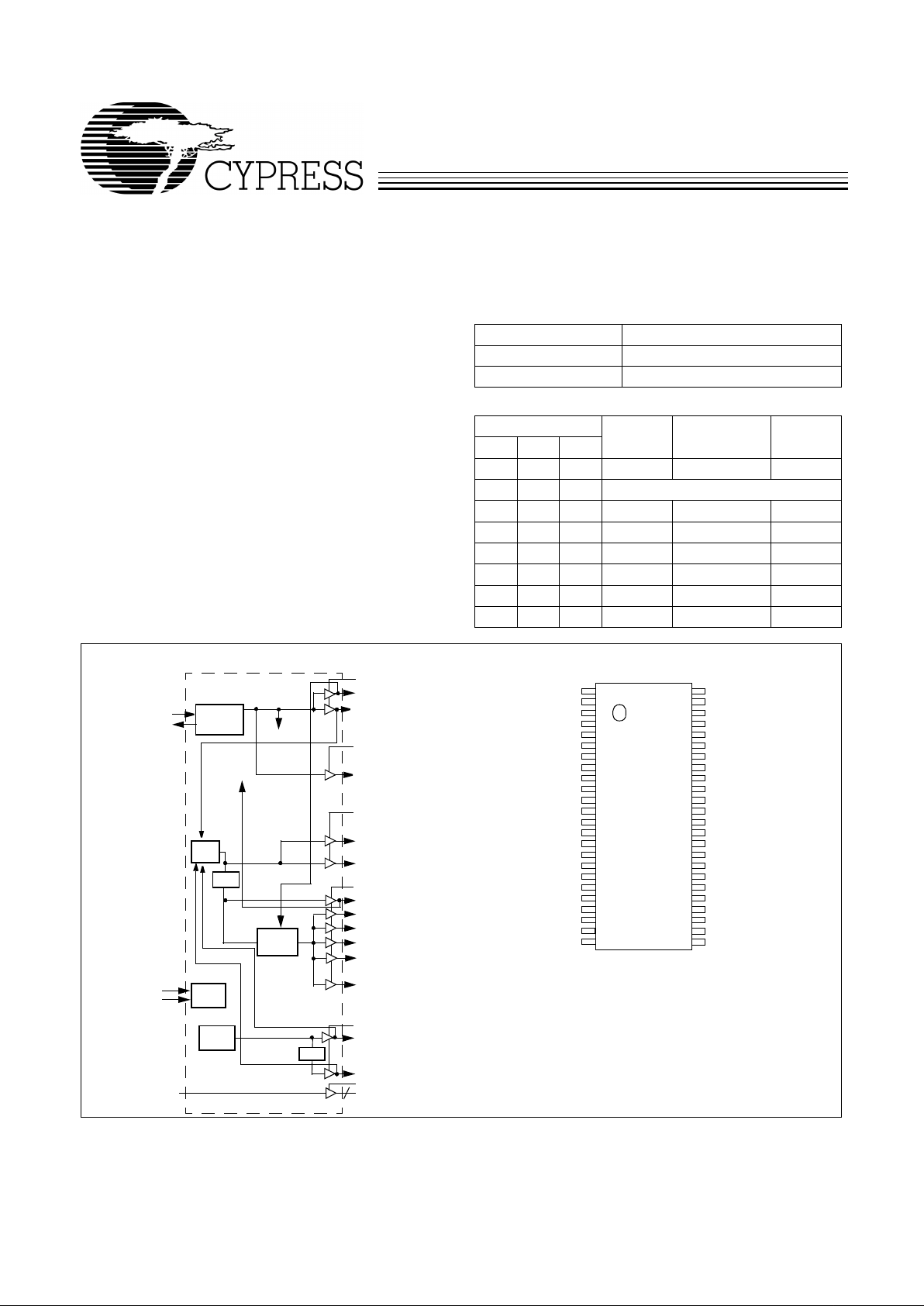
Logic Block Diagram
Pin Configuration
[2]
VDDQ3
REF0/(PCI_STOP#)
VDDQ2
CPU0
PCI_F/MODE
XT AL
PLL Ref Freq
PLL 1
X2
X1
REF1/FS2
VDDQ3
Stop
Clock
Control
PCI2
PCI3
PCI4
48MHz/FS0
24MHz/FS1
PLL2
÷2/÷3
OSC
VDDQ2
VDDQ3
IOAPIC
PCI5
I2C
SDATA
Logic
SCLK
I/O Pin
Control
SDRAM0:12
SDRAMIN
13
VDDQ3
PCI1
CPU1
÷2
VDDQ3
REF0/(PCI_STOP#)
GND
X1
X2
VDDQ3
PCI_F/MODE
PCI1
GND
PCI2
PCI3
PCI4
PCI5
VDDQ3
SDRAMIN
GND
SDRAM11
SDRAM10
VDDQ3
SDRAM9
SDRAM8
GND
SDA TA
SCLK
W149
VDDQ2
IOAPIC
REF1/FS2*
GND
CPU0
CPU1
VDDQ2
OE
SDRAM1 2
GND
SDRAM0
SDRAM1
VDDQ3
SDRAM2
SDRAM3
GND
SDRAM4
SDRAM5
VDDQ3
SDRAM6
SDRAM7
VDDQ3
48MHz/FS0*
24MHz/FS1*
48
47
46
45
44
43
42
41
40
39
38
37
36
35
34
33
32
31
30
29
28
27
26
25
1
2
3
4
5
6
7
8
9
10
11
12
13
14
15
16
17
18
19
20
21
22
23
24
I2C
{
Page 2
W149
2
Pin Definitions
Pin Name Pin No. Pin Type Pin Description
CPU0:1 44, 43 O
CPU Clock Outputs:
See Tables 2 and 6 for detailed f requency informa tion. Output
voltage swing is controlled b y voltage applied to VDDQ2.
PCI1:5 8, 10, 11, 12,
13
O
PCI Clock Outputs 1 through 5:
These five PCI clock outputs are control led by
the PCI_STOP# control pin. Output voltage swing is controlled by voltage applied
to VDDQ3.
PCI_F/MODE 7 I/O
Fixed PCI Clock Output:
Frequency is set by the FS0:1 inputs or through serial
input interface, see Tables 2 and 6. This output is not affected by the PCI_STOP #
input. Upon po wer- up the mode inp ut will be latched, which will determine the f unction of pin 2 , R E F0/(P C I_STOP #). Se e Table 1.
OE 41 I
Output Enable Input:
When brought LOW, all outputs are placed in a high-imped-
ance state. When brought HIGH, all clock outputs activate.
IOAPIC 47 O
IOAPIC Cloc k Output:
Provides 14.31 8-MHz fi xed frequency. The output voltage
swing is controlled by VDDQ2.
48MHz/FS0 26 I/O
48-MHz Output:
48 MHz is provi ded in normal oper ation. In stan dard system s, this
output can be used as the reference for t he Universal Serial Bus. Upon po wer-up,
FS0 input will be latched, which will set clock frequencies as described in Table 2.
This output does not have the Spread Spectrum feature.
24MHz/FS1 25 I/O
24-MHz Output:
24 MHz is provi ded in normal oper ation. In stan dard system s, this
output can be used as the cloc k input f or a Super I/O chip. Upon power-up FS1 inpu t
will be lat ched, wh ich wi ll set cloc k f req uencies as describ ed in Table 2. This outpu t
does not have the Spread Spectrum feature.
REF1/FS2 46 I/O
I/O Dual-Function REF1 and FS2 pin:
Upon power-up, FS2 input will be latched
which will set clock frequencies as described in Table 2. When an outp ut, this pin
provides a fixed clock signal equal in frequency to the reference signal provided at
the X1/X2 pins.
REF0/
(PCI_STOP#)
2I/O
Fixed 14.318-MHz Outpu t 0 or PCI_STOP# Pin:
Function is determined by the
MODE input. When set as an input, the PCI_STOP# input enabl es the PCI 1:5
outputs when HIGH and causes th em to remai n at logic 0 when LOW. The
PCI_STOP signal is latched on the rising edge of PCI_F. Its effects take place on
the next PCI_F clock cycle. When an output, this pin provides a fixed clock signal
equal in frequency to the reference signa l pr ovided at the X1/X2 pins.
SDRAMIN 15 I
Buffered Input Pin:
The signal provided to this input pin is buffered to 13 outputs
(SDRAM0:12).
SDRAM0:12 38, 37, 35,
34, 32, 31,
29, 28, 21,
20, 18, 17, 40
O
Buffered Outputs:
These thirteen dedicated outpu ts provide copies of the signal
provided at the SDRAMIN inpu t. The swing is set by VDDQ3, and they are deactivated when CLK_STOP# input is set LOW.
SCLK 24 I Clock pin for I
2
C circui try.
SDATA 23 I/O Data pi n for I
2
C circuitry.
X1 4 I
Crystal Connection or External Reference Frequency Input:
This pin has dual
functions . It can be used as an external 14.318-MHz crystal connection or as an
external reference frequency input.
X2 5 I
Crystal Connection:
An input connection for an external 14.318-MHz crystal. If
using an external reference, thi s pin must be left unconnected.
VDDQ3 1, 6, 14, 19,
27, 30, 36
P
Po we r Connection:
Po wer supply for core logic, PLL circuitry, SDRAM outputs,
PCI outputs, reference outputs, 48-MHz output, and 24-MHz output. Conn ect to
3.3V supply.
VDDQ2 42, 48 P
Po wer Connection:
Po wer supply for IOAPIC and CPU0: 1 output b uff ers. Con nect
to 2.5V, or 3.3V.
GND 3, 9, 16, 22,
33, 39, 45
G
Ground Connections:
Connect all ground pins to the common system ground
plane.
Page 3
W149
3
Overview
The W149 was developed as a single chip device to meet the
clocking needs of the Intel 440BX AGPset. In addition to the
typical output s prov id ed by st anda rd 100-MHz 440 BX A GPset
FTGs, the W149 adds a thirteen output buffer, supporting
SDRAM DIMM modules in con junction with the chipset.
Cypress proprietary spread spectrum frequency synthesis
technique is a f eature of the CPU and PCI outputs . This featur e
reduces the peak EMI measurements of not only the output
signals and t heir harmonics, but also of an y other cl ock sign als
that are properly synchronized to them.
Functional Description
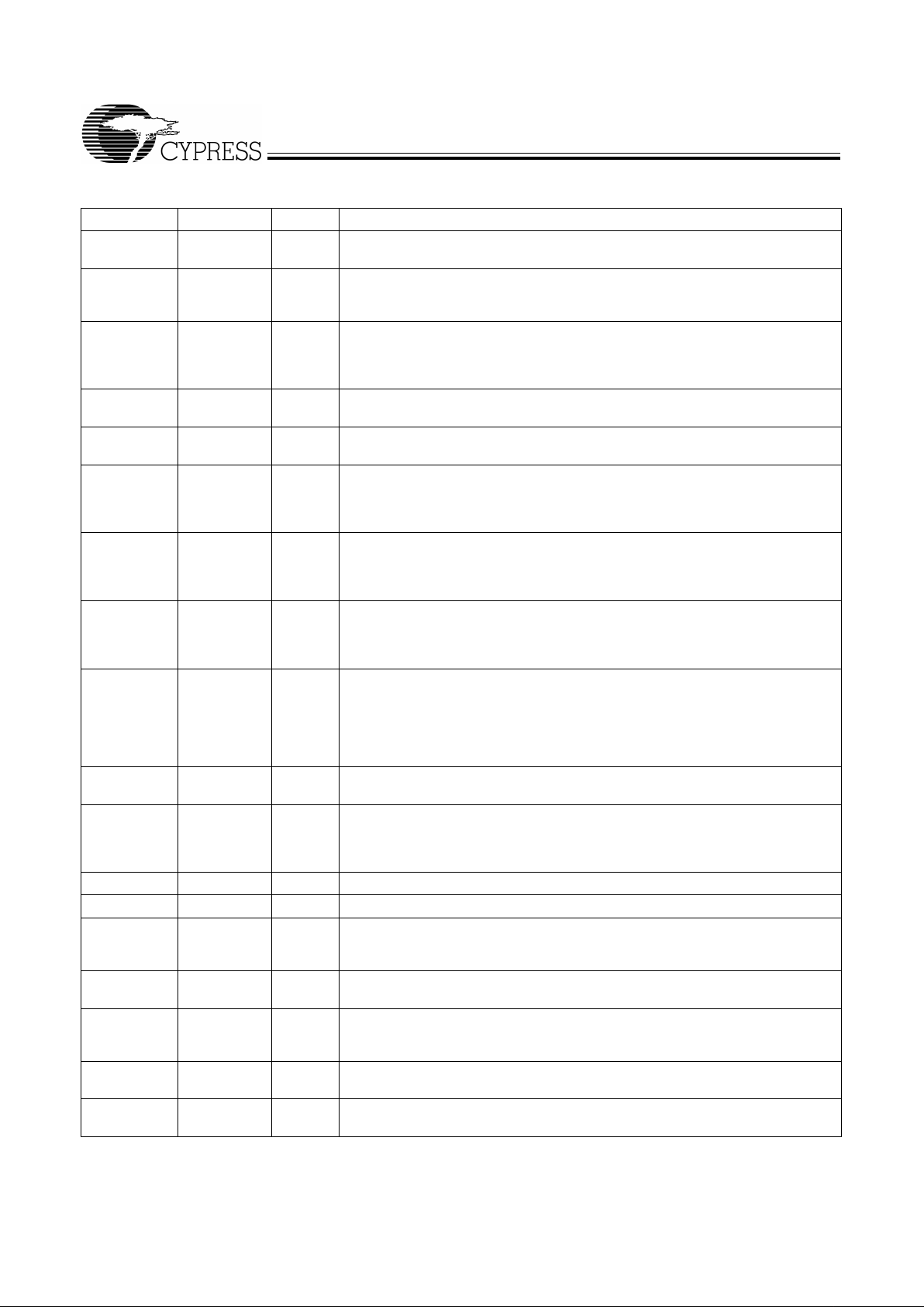
I/O Pin Operation
Pins 7, 25, 26, 46 are dual-purpose l/O pins. Upon power-up
these pins act as logic inputs, allowing the determination of
assigned device functions. A short time after power-up, the
logic state of each pin is latched and the pins become clock
outputs. This feature reduces device pin count by combining
clock outputs with input select pins.
An external 10-kΩ “strapping” resistor is connected between
the l/O pin and ground or V
DD
. Connection to ground sets a
latch to “0”, connection to V
DD
sets a latch to “1”. Figure 1 an d
Figure 2 show two suggested methods for strapping resistor
connections.
Upon W149 power-up, the first 2 ms of operation is used for
input logic selection. During this period, the four I/O pins (7,
25, 26, 46) are three-stated, allowing the output strapping resistor on the l/O pins t o pull each pin and its ass ociated capac itive cloc k load to either a logi c HIGH or LO W st at e. At the end
of the 2-ms period, the establi shed logic “0” or “1” condition of
the l/O pin is latched. Next the output buffer is enabled, converting the l/O p ins i nto oper a ting c loc k ou tputs . The 2-ms timer starts when V
DD
reaches 2.0V. The input bits can only be
reset by turning V
DD
off and then back on again.
It should be noted that the strapping resistors have no significant effect on clock output signal integrity. The drive impedance of clock out put is <40Ω (nominal), which is mini ma ll y affected by the 10-kΩ strap to ground or V
DD
. As wi th the series
termination resistor, the output strapping resistor should be
placed as close to the l/O pin as possible in order to keep the
interconnecting trace short. The trace from the resistor to
ground or V
DD
should be ke pt less t han tw o i nches i n lengt h to
prevent system noise coupling during input logic sampling.
When the clock outputs are enabled following the 2-ms input
period, the specified output frequency is delivered on the pin,
assuming that V
DD
has stabilized. If VDD has not yet reached
full va lue, output frequency initi ally ma y be belo w target b ut will
increase to target once V
DD
voltage has stabilized. In either
case, a short output clock cycle may be produced from the
CPU clock outputs when the outputs are enabled.
Power-on
Reset
Timer
Output Three -state
Data
Latch
Hold
QD
W149
V
DD
Clock Load
10 k
Ω
Output
Buffer
/RDG 2
S
WLRQ
10 k
Ω
/RDG 2SWLRQ
Output
Low
2XW
S
XW 6WUDSSLQJ5HVLVWRU
6HULHV 7HUPLQDWLRQ 5HVLVWRU
Figure 1. Input Logic Selection Through Resistor Load Option
Power-on
Reset
Timer
Output Three-state
Data
Latch
Hold
QD
W149
V
DD
Clock Load
R
10 k
Ω
Output
Buffer
Output
Low
Output Strapping Resistor
Series Termination Resistor
Jumper Options
Resistor Value R
Figure 2. Input Logic Selection Through Jumper Option
Page 4
W149
4
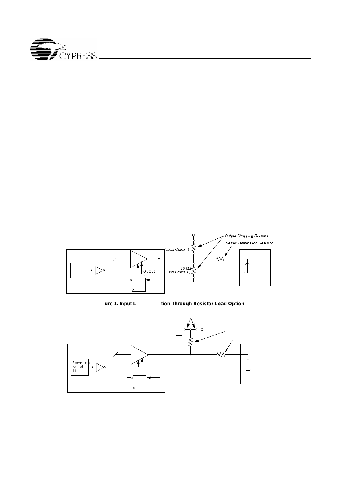
Spread Sp ectrum C locki n g
The device generates a clock that is frequency modulated in
order to increase the bandwidth that it occu pies. By increas ing
the bandwidth of the fundamental and its harmonics, the amplitudes of the radiated electromagnetic emissions are reduced. This effect is depicted in Figure 3.
As shown in Figure 3, a harmonic of a modulated clock has a
much low er amplitude t han that of an un modulated si gnal. The
reduction in amplitude is dependent on the harmonic number
and the frequency deviation or spread. The equation for the
reduction is:
dB = 6.5 + 9*log10(P) + 9*log10(F)
Where 3 is the percentage of deviation and ) is the frequency
in MHz where the reduction is measured.
The output clock is modulated with a waveform depicted in
Figure 4. This waveform, as discussed in “Spread Spectrum
Clock Gener ation f or the Redu ct ion of Radiat ed Emiss ions” by
Bush, Fessler, and Hardin produces the maximum reduction
in the amplitude of radiated electromagnetic emissions. The
deviati on select ed f or this chip is either –0.5% or ±0.5% of the
selected frequency. Figure 4 details the Cypress spreading
pattern. Cypress does offer options with more spread and
greater EMI r eduction. Cont act your local Sal es represen tativ e
for details on these devices.
Spread Spectrum clocking cannot be deactivated on the
W149.
Figure 3. Clock Harmonic with and without SSCG Modul ati on Frequency Domain Representation
SSFTG Typical Clock
Frequency Span (MHz)
Amplitude (dB)
Center Spread
MAX (+0.5%)
MIN (–0.5%)
10%
20%
30%
40%
50%
60%
70%
80%
90%
100%
10%
20%
30%
40%
50%
60%
70%
80%
90%
100%
FREQUENCY
Figure 4. Typical Modulation Profile
Page 5
W149
5
Serial Data Interface
The W149 features a two-pin, serial data interf ace that can b e
used to configure internal register settings that control particular de vice func tions. Upon power -up , the W149 i nitiali zes wit h
default register settings, therefore the use of this serial data
interface is optional. The serial interface is write-only (to the
clock chi p) and is t he dedica ted func tion of de vice pins SD ATA
and SCLOCK. In motherboard applications, SDATA and
SCLOCK are typically driven by two logic outputs of the
chipset. Clock device register changes are normally made
upon system initialization, if any are required. The interface
can also be used durin g system operation for power management functions. Tab l e 3 summarizes the control functions of
the serial data interface.
Operation
Data is written to the W149 in eleven bytes of eight bits each.
Bytes are written in the order sho w n in Table 4.
Table 3. Serial Data Interface Contr ol Functions Summary
Control Function Description Common Application
Clock Output Disable Any individual clock output(s) can be disabled.
Disabled out puts are actively held LOW .
Unused outputs are disabled to reduce EMI
and system power. Examples are clock
outputs to unus ed PCI slots.
CPU Clock Frequency
Selection
Provides CPU/PCI fr equency selections throug h
software. Frequency is changed in a smooth and
controlled fashion.
For alternate microprocessors and power
management options. Smooth frequency
transition allows CPU frequency change
under normal system operation.
Output Three-st ate Puts clock out put into a high-impedance st ate. Production PCB testi ng.
(Reserved) Reserved functi on for future dev ice revision or
production device testing.
No user application. Register bit must be
written as 0.
Table 4. Byte Writing Sequence
Byte
Sequence Byte Name Bit Sequence Byte Description
1 Slave Address 11010010 Commands the W149 to accept the bi ts in Data Bytes 0–6 for internal
register co nfigurati on. Since othe r devi ces may exist on the same common serial data bus, it is ne cessary to hav e a specific slav e address f or
each potential receiver. The slave recei ver address f or the W149 is
11010010. Regist er setting wi ll not be made if the Slav e Addr ess is not
correct (or is for an alternate slave receiver).
2 Command Code Don’t Care Unused by the W149, therefore bit values are ignored (“Don’t Care”).
This byte must be included in the data write sequence to maintain prop er byte allocation. The Command Code Byte is part of the standard
serial communi ca tion protoc ol and ma y be use d wh en writi ng t o a nother addressed slave receiver on the serial data bus.
3 Byte Count Don’t Care Un used by the W149, therefore bit values are ignored (“Don’t Care”).
This byte must be included in the data write sequence to maintain prop er byte allocation. The Byte Count Byte is part of the standard serial
communication protocol and may be used when writing to another addressed slave receiver on the serial data bus.
4 D ata Byte 0 Refer to Table 5 The data bit s in Data Bytes 0–7 s et internal W149 register s that c ontrol
device operation. The data bits are only accepted when the Address
Byte bit seq uence is 11010010, as noted above. For description of bit
control f unctions, refer to Table 5, Data Byte Serial Configuration Map.
5 D ata Byte 1
6 D ata Byte 2
7 D ata Byte 3
8 D ata Byte 4
9 D ata Byte 5
10 Data Byte 6
11 Data Byte 7
Page 6

W149
6
Writing Data Bytes
Each bit in Data Bytes 0–7 control a particular device fu nction
excep t for the “reserved” bits which must be written as a logic
0. Bits are wri tten MSB (most significa nt bit) fi rst, which is bit 7.
Table 5 gives the bit formats fo r registers lo cated in Data Bytes
0–7.
Tabl e 6 details additional frequency selections that are available through t he seri al dat a interface.
Table 7 details the select functions for Byte 0, bits 1 and 0.
Table 5. Data Bytes 0–7 Serial Configuration Map
Bit(s)
Affected Pin
Control Function
Bit Control
DefaultPin No. Pin Name 0 1
Data Byte 0
7-- --Don’t Care -- -- 0
6 -- -- SEL_2 See Table 6 0
5 -- -- SEL_1 See Table 6 0
4 -- -- SEL_0 See Table 6 0
3 -- -- Hardware/Softwar e Frequency Select Hardware Software 0
2-- --Don’t Care -- -- 0
1–0-- -- Bit 1
Bit 0 Function (See Table 7 for fu n c tion details)
0 0 Normal Operation
0 1 (Reserved)
1 0 Normal Operation
1 1 All Outputs Three-stated
00
Data Byte 1
7 -- -- (Reserved) -- -- 0
6 -- -- (Reserved) -- -- 0
5 -- -- (Reserved) -- -- 0
4 -- -- (Reserved) -- -- 0
3 40 SDRAM12 Clock Output Disable Low Active 1
2 -- -- (Reserved) -- -- 0
1 43 CPU1 Clock Output Disable Low Active 1
0 44 CPU0 Clock Output Disable Low Active 1
Data Byte 2
7 -- -- (Reserved) -- -- 0
6 7 PCI_F Clock Output Disable Low Active 1
5 -- -- (Reserved) -- -- 0
4 13 PCI5 Clock Output Disable Low Active 1
3 12 PCI4 Clock Output Disable Low Active 1
2 11 PCI3 Clock Output Disable Low Active 1
1 10 PCI2 Clock Output Disable Low Active 1
0 8 PCI1 Clock Output Disable Low Active 1
Data Byte 3
7 -- -- (Reserved) -- -- 0
6 -- -- (Reserved) -- -- 0
5 26 48MHz Clock Output Disable Low Active 1
4 25 24MHz Clock Output Disable Low Active 1
3 -- -- (Reserved) -- -- 0
2 21, 20,
18, 17
SDRAM8:11 Clock Output Disable Low Active 1
Page 7

W149
7
1 32, 31,
29, 28
SDRAM4:7 Clock Output Disable Low Active 1
0 38, 37,
35, 34
SDRAM0:3 Clock Output Disable Low Active 1
Data Byte 4
7 -- -- (Reserved) -- -- 0
6 -- -- (Reserved) -- -- 0
5 -- -- (Reserved) -- -- 0
4 -- -- (Reserved) -- -- 0
3 -- -- (Reserved) -- -- 0
2 -- -- (Reserved) -- -- 0
1 -- -- (Reserved) -- -- 0
0 -- -- (Reserved) -- -- 0
Data Byte 5
7 -- -- (Reserved) -- -- 0
6 -- -- (Reserved) -- -- 0
5 -- -- (Reserved) -- -- 0
4 47 IOAPIC Clock Output Disab le Low Active 1
3 -- -- (Reserved) -- -- 0
2 -- -- (Reserved) -- -- 0
1 46 REF1 Clock Output Disable Low Active 1
0 2 REF0 Clock Output Disab le Low Active 1
Data Byte 6
7 -- -- (Reserved) -- -- 0
6 -- -- (Reserved) -- -- 0
5 -- -- (Reserved) -- -- 0
4 -- -- (Reserved) -- -- 0
3 -- -- (Reserved) -- -- 0
2 -- -- (Reserved) -- -- 0
1 -- -- (Reserved) -- -- 0
0 -- -- (Reserved) -- -- 0
Data Byte 7
7 -- -- (Reserved) -- -- 0
6 -- -- (Reserved) -- -- 0
5 -- -- (Reserved) -- -- 0
4 -- -- (Reserved) -- -- 0
3 -- -- (Reserved) -- -- 0
2 -- -- (Reserved) -- -- 0
1 -- -- (Reserved) -- -- 0
0 -- -- (Reserved) -- -- 0
Table 5. Data Bytes 0–7 Serial Configuration Map
(continued)
Bit(s)
Affected Pin
Control Function
Bit Control
DefaultPin No. Pin Name 0 1
Page 8

W149
8
Table 6. Additional Frequency Sele cti ons through Serial Data Interface Data Byt es
[3]
Input Conditions Output Frequency Spread %
Data Byte 0, Bit 3 = 1
CPU0:1,
SDRAM0:12 (MHz)
PCI_F, 1:5
(MHz)
Bit 6
SEL_2
Bit 5
SEL_1
Bit 4
SEL_0
1 1 1 100. 2 33.4 –0.5
1 1 0 (Reserved) (Reserved) (Reserved)
1 0 1 100 33.3 ±0.5
1 0 0 103 34.3 –0.5
0 1 1 66.8 33.4 –0.5
0 1 0 83.3 41.65 –0.5
0 0 1 66.8 33.4 ±0.5
0 0 0 124 41.3 –0.5
Table 7. Select Function for Data Byte 0, Bit s 0:1
Function
Input Conditions Output Conditions
Data Byte 0
CPU0:1
PCI_F,
PCI1:5
REF0:1,
IOAPIC 48MHZ 24MHZBit 1 Bit 0
Normal Operation X 0 Note 1 Note 1 14.318 MHz 48 MHz 24 MHz
Three-state 1 1 Hi-Z Hi-Z Hi-Z Hi-Z Hi-Z
Note:
3. CPU and PCI frequency selections are listed in
Table 2
and
Table 6
.
Page 9

W149
9
Absolute Maximum Ratings
Stresses greater than those listed in this table may cause permanent damage to the de vice . These represent a stress ratin g
only. Operation of the device at these or any other conditions
above those specified in the operating sections o f t his specification is not implied. Maximum conditions for extended periods may affect reliabili ty.
.
Parameter Description Rating Unit
V
DD
, V
IN
Voltage on any pin with res pect to GND –0.5 to +7 .0 V
T
STG
Storage Temperature –65 to +150 °C
T
B
Ambient Temperature under Bias –55 to +125 °C
T
A
Operating Temperature 0 to +70 °C
ESD
PROT
Input ESD Protection 2 (min) kV
DC Electr i cal C h ar acteristi cs:
T
A
= 0°C to +70°C; V
DDQ3
= 3.3V±5%; V
DDQ2
= 2.5V±5%
Parameter Description T est Condition Min. Typ. Max. Unit
Supply Current
I
DD
3.3V Supply Current CPU0:1 = 100 MHz
Outputs Loaded
[4]
260 mA
I
DD
2.5V Supply Current CPU0:1 = 100 MHz
Outputs Loaded
[4]
25 mA
Logic Inputs
V
IL
Input Low Voltage GND – 0.3 0.8 V
V
IH
Input High Voltage 2.0 VDD + 0.3 V
I
IL
Input Low Current
[5]
–25 µA
I
IH
Input High Current
[5]
10 µA
Clock Outputs
V
OL
Output Low Voltage IOL = 1 mA 50 mV
V
OH
Output High Voltage IOH = 1 mA 3.1 V
V
OH
Output High Voltage CPU0:1,
IOAPIC
IOH = –1 mA 2.2 V
I
OL
Output Low Current CPU0:1 VOL = 1.25V 27 57 97 mA
PCI_F, PCI1:5 V
OL
= 1.5V 20.5 53 139 mA
IOAPIC V
OL
= 1.25V 40 85 140 mA
REF0:1 V
OL
= 1.5V 25 37 76 mA
48MHz V
OL
= 1.5V 25 37 76 mA
24MHz V
OL
= 1.5V 25 37 76 mA
I
OH
Output High Current CPU0:1 VOH = 1.25V 25 55 97 mA
I
OH
Output High Current PCI_F, PCI1:5 VOH = 1.5V 31 55 139 mA
IOAPIC V
OH
= 1.25V 40 87 155 mA
REF0:1 V
OH
= 1.5V 27 44 94 mA
48MHz V
OH
= 1.5V 27 44 94 mA
24MHz V
OH
= 1.5V 25 37 76 mA
Notes:
4. All clock outputs loaded with 6" 60Ω traces with 22-pF capacitors.
5. W149 logic inputs have internal pull-up devices (pull-ups not full CMOS level).
Page 10

W149
10
AC Electrical Characteristics
TA = 0°C to +70°C; V
DDQ3
= 3.3V±5%; V
DDQ2
= 2.5V±5%; f
XTL
= 14.31818 MHz
AC clock parameters are tested and guaranteed over stated operating conditions using the stated lump capacitive load at the
clock output; Spread Spectrum clocking is disabled.
Crystal Oscillator
V
TH
X1 Input threshold Volt age
[6]
V
DDQ3
= 3.3V 1.65 V
C
LOAD
Load Capacitance, Imposed on
External Crystal
[7]
14 pF
C
IN,X1
X1 Input Capacitance
[8]
Pin X2 unconnected 28 pF
Pin Capacitance/Induct ance
C
IN
Input Pin Capacitance Except X1 and X2 5 pF
C
OUT
Output Pin Capacitance 6pF
L
IN
Input Pin Inductance 7nH
Notes:
6. X1 input threshold voltage (typical) is V
DDQ3
/2.
7. The W149 contains an internal crystal load capacitor between pin X1 and ground and another between pin X2 and ground. Total load placed on crystal is
14 pF; this includes typical stray capacitance of short PCB traces to crystal.
8. X1 input capacitance is applicable when driving X1 with an external clock source (X2 is left unconnected).
DC Electr i cal C h ar acteristi cs:
(continued) T
A
= 0°C to + 70°C; V
DDQ3
= 3.3V±5%; V
DDQ2
= 2.5V±5%
Parameter Description T est Condition Min. Typ. Max. Unit
CPU Clock Outputs, CPU_F, CPU1 (Lump Capacitance Test Load = 20 pF)
Parameter Description Test Conditi on/Comments
CPU = 66.6 MHz CPU = 100 MHz
UnitMin. Typ. Max. Min. Typ. Max.
t
P
P eriod Measured on rising edge at 1.25V 15 15.5 10 10.5 ns
t
H
High Time Duration of clock cycle above 2.4V, at
min. edge rate (1.5 V/ns)
5.6 3.3 ns
t
L
Low Time Duration of clock cycle below 0.4V, at
min. edge rate (1.5 V/ns)
5.3 3.1 ns
t
R
Output Rise Edg e Rate Mea sur ed from 0.4V to 2.4V 1.5 4 1.5 4 V/ns
t
F
Output Fall Edge Rate Measured from 2.4V to 0.4V 1.5 4 1.5 4 V/ns
t
D
Duty Cycle Measured on rising and falling edge at
1.5V, at min. edge rate (1.5 V/ns)
45 55 45 55 %
t
JC
Jitter , Cycle-to-Cycl e Measured on rising edge at 1.25V. Max-
imum difference of cycle time between
two adjacent cycles.
200 200 ps
t
SK
Output Skew Measured on rising edge at 1.5V 250 250 ps
f
ST
Frequency Stabilization from Power-up
(cold start)
Assumes full supply voltage reached
within 1 ms from p ower-up . Short cycles
exist prior to frequency stabilization.
33ms
Z
o
AC Output Impedance Average value during switching transi-
tion. Used for determining series te rmination value.
20 20 Ω
Page 11

W149
11
SDRAM Clock Outputs, SDRAM, SDRAM0:11 (Lump Capacitance Test Load = 30 pF)
Parameter Description Test Condition/Comments
CPU = 66.6 MHz CPU = 100 MHz
UnitMin. Typ. Max. Min. Typ. Max.
t
P
P eriod Measured on rising edge at 1.5V 30 30 ns
t
H
High Time Duration of clock cy cle abov e 2.4V,
at min. sdge rate (1.5 V/ns)
5.6 3.3 ns
t
L
Low Time Duration of cloc k cycle be low 0.4V,
at min. sdge rate (1.5 V/ns)
5.3 3.1 ns
t
R
Output Rise Edge
Rate
Measured from 0.4V to 2.4V 1.5 4 1.5 4 V/ns
t
F
Output Fall Edge
Rate
Measured from 2.4V to 0.4V 1.5 4 1.5 4 V/ns
t
PLH
Prop Delay LH Input edge rate faster than 1 V/ns 1 5 1 5 ns
t
PHL
Prop Delay HL Input edge rate faster than 1 V/ns 1 5 1 5 ns
t
D
Duty Cycle Measured on rising and falling
edge at 1.5V, at min. sdge rate
(1.5 V/ns)
45 55 45 55 %
t
JC
Jitter, Cycle-to-Cycle Measured on rising edge at 1.5V.
Maximum difference of cycle time
between two adjacent cycles.
250 250 ps
t
SK
Output Skew Measured on rising edg e at 1.5V 250 250 ps
t
O
CPU to PCI Clock
Skew
Covers al l CPU/ PCI outputs. Measured on rising edge at 1.5V. CPU
leads PCI output.
1.5 4 1.5 4 ns
f
ST
Frequency
Stabilization from
P ower-up (cold start)
Assumes full supply voltage
reached within 1 ms from
power-up. Short cycles exist prior
to frequency stabilization.
33ms
Z
o
AC Output
Impedance
Av erage value during switching
transition. Used for determining
series termination val ue.
30 30 Ω
Page 12

W149
12
PCI Clock Outputs, PCI_F and PCI1:5 ( Lum p Capacit ance Test Load = 30 pF)
Parameter Description Te st Condi tion/Comments
CPU = 66.6/100 MHz
UnitMin. Typ. Max.
t
P
Period Measured on rising edge at 1.5V 30 ns
t
H
High Time Duration of clock cycle above 2.4V 12.0 ns
t
L
Low Time Duration of clock cycle below 0.4V 12.0 ns
t
R
Output Rise Edge Rate Measured from 0.4V to 2.4V 1 4 V/ns
t
F
Output Fall Edge Rate Measured from 2.4V to 0.4V 1 4 V/ns
t
D
Duty Cycle Measured on rising and f alling edg e at 1.5V 45 55 %
t
JC
Jitter , Cycle-to-Cycle Measured on rising e dge at 1.5V. Maximum
difference of cycle time between two adjacent cycles.
250 ps
t
SK
Output Skew Measured on rising edge at 1.5V 500 ps
t
O
CPU to PCI Clock Skew Covers all CPU/PCI outputs. Measured on
rising edge at 1.5V. CPU leads PCI output.
1.5 4 ns
f
ST
Frequency Stabilization
from P ower-up (co ld start)
Assumes full supp ly voltage reach ed within
1 ms from power -up. Short cycles exist prior to frequency stabi lization.
3ms
Z
o
AC Output Impedance Average value during switching tran sition.
Used for det ermini ng series termination
value.
30 Ω
IO APIC Clock Output (Lump Capacitance Test Load = 20 pF)
Parameter Description Test Condition/Comments
CPU = 66.6/100 MHz
UnitMin. Typ. Max.
f Frequency, Actual Frequency generated by crystal oscillator 14.31818 MHz
t
R
Output Rise Edge Rate Measured from 0.4V to 2.0V 1 4 V/ns
t
F
Output Fall Edge Rate Measured from 2.0V to 0.4V 1 4 V/ns
t
D
Duty Cycle Measured on rising and falling edge at 1.25V 45 55 %
f
ST
Frequency Stabilization
from Po wer-up (cold st art)
Assumes full supply voltage reached within
1 ms from power-up. Short cycles exist prior
to frequency stabilization.
1.5 ms
Z
o
AC Output Imp edance Average value during switching transiti on.
Used for determining serie s termination value.
15 Ω
REF0:1 Clock Output (Lump Capacitance Test Load = 20 pF)
Parameter Description Test Condition/Comments
CPU = 66.6/100 MHz
UnitMin. Typ. Max.
f Frequency, Actual Frequency generated by crystal oscillator 14.318 MHz
t
R
Output Rise Edge Rate Measured from 0.4V to 2.4V 0.5 2 V/ns
t
F
Output Fall Edge Rate Measured from 2.4V to 0.4V 0.5 2 V/ns
t
D
Duty Cycle Measured on rising and falling edge at 1.5V. 45 55 %
f
ST
Frequency St abil ization
from Power-up (cold
start)
Assumes full suppl y v oltage reac hed withi n 1 ms from
power-up. Short cycles exist prior to frequency stabilization.
3ms
Z
o
AC Output Impedance Av er age v al ue duri ng s wi tching tra nsi tion. Us ed f or de-
termining series termination value.
40 Ω
Page 13

W149
13
Document #: 38-00856-A
48-MHz Clock Output (Lump Capacitance Test Load = 20 pF= 66.6/100 MHz
Parameter Description Test Condition/Comments
CPU = 66.6/100 MHz
UnitMin. Typ. Max.
f Frequency, Actual Determined by PLL divi der ratio (see m/n below) 48. 008 MHz
f
D
Deviati on from 48 MHz (48. 008 – 48)/48 +167 ppm
m/n PLL Ratio (14.31818 MHz x 57/17 = 48.008 MHz) 57/17
t
R
Output Rise Edge
Rate
Measured from 0.4V to 2.4V 0.5 2 V/ns
t
F
Output Fall Edge Rate Measured from 2.4V to 0.4V 0.5 2 V/ns
t
D
Duty Cycle Measured on rising and fal ling edge at 1.5V 45 55 %
f
ST
Frequency Stabiliza-
tion from Power-up
(cold start)
Assumes full supply volt age reached within 1 ms f rom
power -up. Short cycles exi st prior to frequency stabilization.
3ms
Z
o
AC Output Impedance A verage val ue during s witch ing tr ansit ion. Used f or de-
termining series termination value.
40 Ω
24-MHz Clock Output (Lump Capacitance Test Load = 20 pF= 66.6/100 MHz
Parameter Description Test Condition/Comments
CPU = 66.6/100 MHz
UnitMin. Typ. Max.
f Frequency, Actual Determined by PLL divider ratio (see m/n below) 24.004 MHz
f
D
Deviation from 24 MHz (24.004 – 24)/24 +167 ppm
m/n PLL Ratio (14.31818 MHz x 57/34 = 24.004 MHz) 57/34
t
R
Output Rise Edge Rate M easured from 0.4V to 2.4V 0.5 2 V/ns
t
F
Output Fall Edge Rate Measured from 2.4V to 0.4V 0.5 2 V/ns
t
D
Duty Cycle Measured on rising and falling edge at 1. 5V 45 55 %
f
ST
Frequency Stabiliza-
tion from Power-up
(cold start)
Assumes full supply v ol tage rea ched withi n 1 ms from
power-up. Short cycles exist prior to frequency stabilization.
3ms
Z
o
AC Output Impedance Aver age v alue during s witc hing tr a nsition. Used f or de-
termining series termination value.
40 Ω
Ordering Information
Ordering Code
Package
Name Package Type
W149 H 48-Pin SSOP (300-mil)
Page 14

W149
© Cypress Semiconductor Corporation, 2000. The information contained herein is subject to change without notice. Cypress Semiconductor Corporation assumes no responsibility for the use
of any circuitry other than circuitry embodied in a Cypress Semiconductor product. Nor does it conv ey or imply any lice nse under patent or other rights. Cypress Semiconductor does not authorize
its products for use as critical components in life-support systems where a malfunction or failure may reasonably be expected to result in significant injury to the user. The inclusion of Cypress
Semiconductor products in life-support systems application implies that the manufacturer assumes all risk of such use and in doing so indemnifies Cypress Semiconductor against all charges.
Package Diagram
Summary of nominal dimensions in inches:
Body Width: 0.296
Lead Pitch: 0.025
Body Length: 0.625
Body Height: 0.102
48-Pin Shrink Small Outline Package (SSOP, 300 mils)
 Loading...