

Page 1
W137
Bx Notebook System Frequency Synthesizer
Features
• Maximized EMI suppression usi ng Cypress’s Spread
Spectrum Technology
• T wo copies of CPU output
• Six copies of PCI output (Synch ronous w/CPU output)
• One 48-MHz output for USB support
• One selectable 24-/48-MHz output
• T w o Buffered copies of 14.318-MHz input reference
signal
• Supports 100-MHz or 66-MHz CPU opera ti on
• Power man agement control input pins
• Av ailable in 28-pin SSOP (209 mils)
• SS function can be disabled
• See W40S11-02 for 2 SDRAM DIMM support
Key Specific ati o n s
Supply Voltages:.......................................V
CPU0:1 Output to Output Skew: ........................ ........ 175 ps
CPU0:1 Cycle to Cycle Jit ter:............... .. .................... 200 ps
V
DDQ3
DDQ2
= 3.3V±5%
= 2.5V±5%
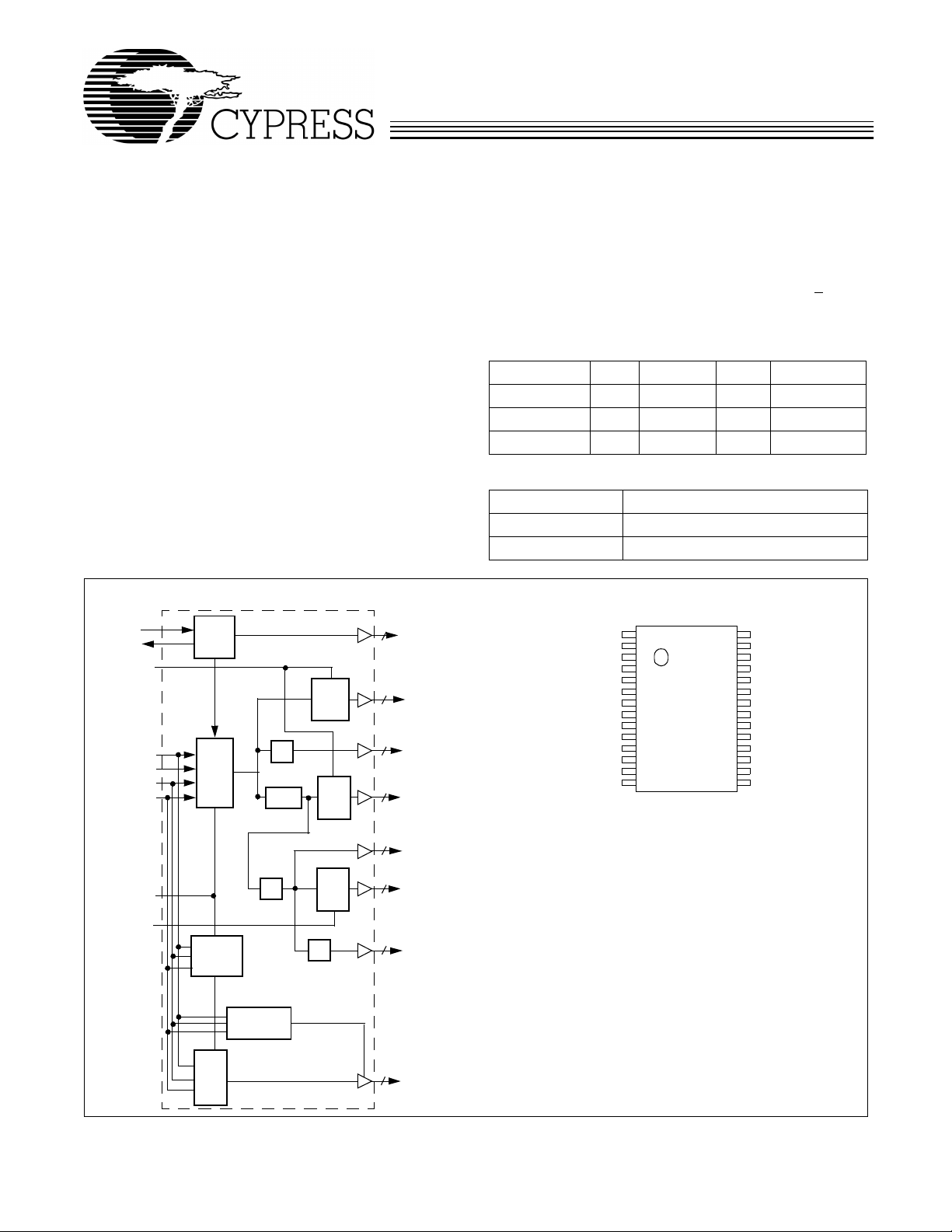
Block Diagram
X1
X2
CPU_STOP#
SPREAD#
SEL0
SEL1
SEL133/100#
XTAL
OSC
PLL 1
÷2
÷2/÷1.5
STOP
Clock
Logic
STOP
Clock
Logic
2
4
2
4
REF0:1
CPU0:3
CPUdiv2_0:1
3V66_0:3
PCI_ F, PCI1:5 Out p u t to Ou tp u t Skew : ... .............. ... ....5 0 0 ps
PCI_ F, PCI1:5 Cyc le to Cy c le Jit te r: .. .............. ... .........250 ps
CPU to PCI Output Skew: ...............1.5–4 .0 ns (CPU Leads)
Output Duty Cycle:.................................................... 45/55%
PCI_F, PCI Edge Rate:............................ .. ............... .>
1 V/ns
CPU_STOP#, OE, SPREAD#, SEL48#, PCI_STOP#,
PWR_DWN# all have a 250-kΩ pull-up resistor.
T able 1. Pin Selectable Frequency
SEL100/66# OE CPU PCI Spread%
0/1 0 HI-Z HI-Z Don’t Care
0 1 66.6 MHz 33.3 See
1 1 100 MHz 33.3 See
Table 2
Table 2
Table 2. Spread Spectrum Feature
SPREAD# Spread Profile
0 –0.5% (down spread)
1 0% (spread disable d)
Pin Configuration
GND
X1
X2
PCI_F
PCI1
PCI2
GND
VDDQ3
PCI3
PCI4
PCI5
VDDQ3
48MHz
24/48MHz/OE
1
2
3
4
5
6
7
8
9
10
11
12
13
14
VDDQ3
28
REF0/SEL48#
27
REF1/SPREAD#
26
VDDQ2
25
CPU0
24
CPU1
23
GND
22
GND
21
PCI_STOP#
20
VDDQ3
19
CPU_STOP#
18
PWR_DWN#
17
SEL100/66#
16
15
GND
PWRDWN#
PCI_STOP#
Power
Down
Logic
PLL2
÷2
Three-state
Logic
÷2
Cypress Semiconductor Corporation
1
PCI_F
STOP
Clock
Logic
7
3
1
PCI1:7
IOAPIC0:2
48MHz
• 3901 North First Street • San Jose • CA 95134 • 408-943-2600
October 12, 1999, r ev . **
Page 2
Pin Definitions
Pin Name
CPU0:1 24, 23 O
PCI1:5 5, 6, 9, 1 0 , 11O
PCI_F 4 O
CPU_STOP# 18 I
PCI_STOP# 20 I
REF0/SEL48# 27 I/O
REF1/SPREAD# 26 I/O
24/48MHz/OE 14 I/O
48MHz 13 O
SEL100/66# 16 I
X1 2 I
X2 3 I
PWR_DWN# 17 I
VDDQ3 8, 12, 19, 28 P
VDDQ2 25 P
GND 1, 7, 15, 21, 22G
Pin
No.
Type Pin Description
Pin
CPU Clock Outputs 0 and 1:
These two CPU clock out puts are controlled by th e
CPU_STOP# control pin. Output volta ge swing is controlled by voltage app li ed to
VDDQ2. Frequency is selected per Table 1.
PCI Bus Clock Outputs 1 through 5:
These five PCI clock outputs are controlled
by the PCI _ST OP# contr ol p in. Outpu t v ol tage s wing is co ntr olle d by v o ltage appli ed
to VDDQ3. Frequency is selected per Table 1.
Fixed PCI Clock Output:
Unlike PCI1:5 outp uts, this output is not controlled b y the
PCI_STOP# control pin; it cannot be forced LOW by PCI_STOP#. Output voltage
swing is control led by vol tage appl ied to VDDQ3. F req uency is selected per Table 1.
CPU_STOP# Input:
When brought LOW, clock outputs CPU0:1 are stopped LOW
after completi ng a full clock cycl e (2–3 CPU cloc k latency). When brought HIGH,
clock outputs CPU0:1 start with a full cloc k cycle (2–3 CPU cl o ck l a tency).
PCI_STOP# Input :
The PCI_STO P# input enables the PCI1:5 outputs when HIGH
and causes them to remai n at logi c 0 when LO W. The PCI_STOP# signa l is latc hed
on the rising edge of PCI_F. Its effect takes place on the next PCI_F clock cycle.
I/O Dual-Function REF0 and SEL48# Pin:
latched. The state i s set b y either a 10K resis tor to GND or to V
GND causes pin 14 to provide a 48-MHz clock. If the pi n is strapped to V
Upon power-up, the state of SEL48# is
. A 10K resistor to
DD
will provide a 24-MHz cl ock. After 2 ms, the pin becomes a high-drive output that
produces a copy of 14.318 MHz.
I/O Dual-Function REF1 and SPREAD# Pin:
Upon power-up, the state of
SPREAD# is latched. The state is set by either a 10K resistor to GND or to V
10K resistor to GND enables Spr ead Spectrum function. If the pin is str apped to V
Spread Spectrum is disabled. After 2 ms, the pin beco me s a high- drive output that
produces a copy of 14.318 MHz.
I/O Dual-Function 24-MHz or 48-MHz Output and Output Enable Input:
power-up, the state of pin 14 is latched. The state is set by either a 10K resistor to
GND or to V
stated. If the pin is strapped to V
. A 10K resistor to GND latches OE LOW, and all outputs are three-
DD
, OE is latched HIGH and all outputs are active.
DD
After 2 ms, the pin becomes an out put whose freque ncy is set b y the state of pin 27
on power-up.
48-MHz Output:
Fixed 48-MHz USB output. Output voltage swing is controll ed by
voltage applied to VDDQ3.
Frequency Selecti on Input:
Select power -up default CPU cloc k frequency as shown
in Table 1 .
Crystal Connection or External Ref erence Frequency Input:
This pin can either
be used as a connection to a crystal or to a reference signal.
Crystal Connection:
An input connection for an external 14.318-MHz crystal. If
using an external reference, this pin must be left unconnected.
Power Down Contr ol:
When thi s input is LO W , de vice goes in to a low-p ower standb y
condition. All outputs are held LOW. CPU and PCI clock outputs are stopped LOW
after completi ng a full clock cycl e (2–3 CPU clock cycle latency). When brought
HIGH, CPU and PCI outputs start with a full cloc k cycle at full operating frequency
(3 ms maximum latency).
Power Connection:
Power Connection:
Ground Connection:
Connected to 3.3V.
Power suppl y for CPU0:1 output buffers. Connected to 2.5V.
Connect all gro und pins t o the comm on syst em g round pl an e.
W137
, pin 14
DD
DD
Upon
. A
DD
,
2
Page 3
W137
Overview
The W137 was developed to meet the Intel® Mobile Clock
specification for the BX chipset, including Super I/O and USB
support. The W40S11-02 is the Intel-defined companion part
used for driving 2 SDRAM DIMM modules. Please see that
data sheet for additional information.
Cypress’s proprietary spread spectrum frequency synthesis
technique is a feature of the CPU and PCI outputs. When enabled, th is feat ure reduces the peak EMI measurement s of not
only the output signals and their harmonics, but also of any
other clock signals that are properly synchronized to them.
The –0 .5% modulation pr ofile match es that defined as accep table in Intel’s clock specification.
Functional Description
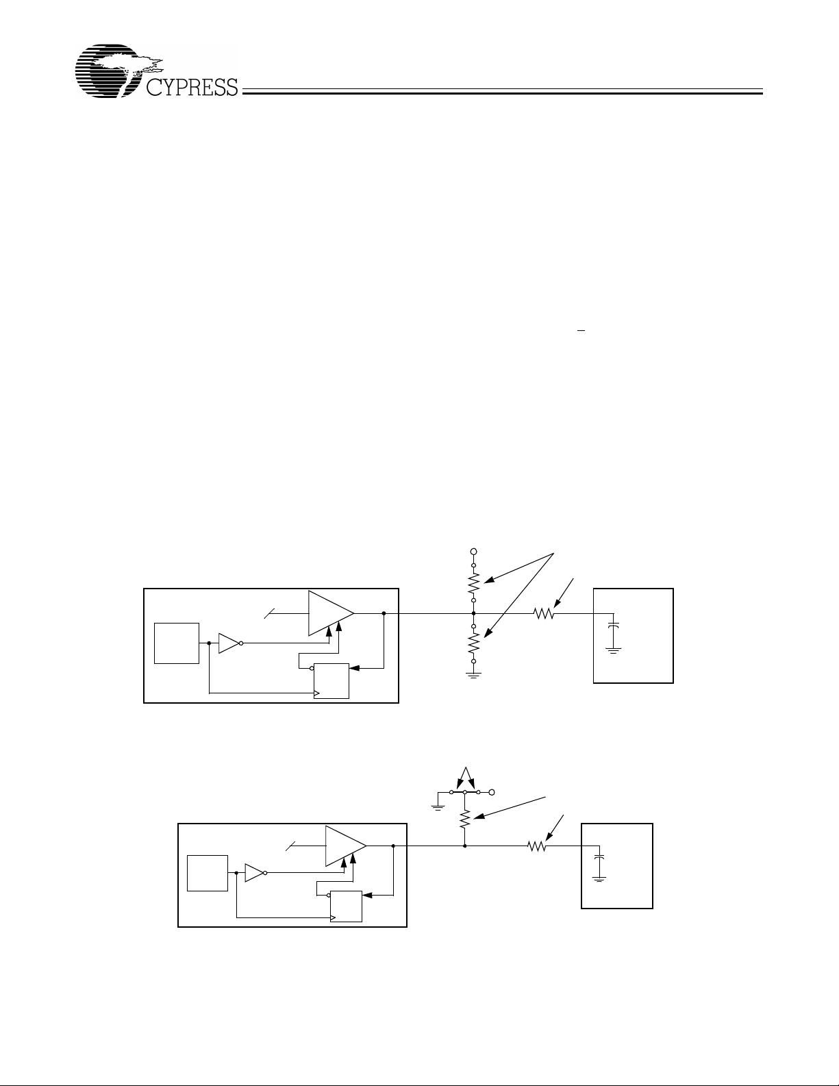
I/O Pin Operation
Pins 14, 26, and 27 ar e dua l-purpose l/ O pins . Upon po wer -up
these pins act as logic inputs, allowing the determination of
assigned device functions. A short time after power-up, the
logic state of each pin is latched and the pins then become
clock outputs. This feature reduces device pin count by combining cloc k outputs with input selec t pins.
An external 10-kΩ “strapping” resistor is connected between
each l/O pin and ground or V
latch to “0”, connect ion to V
. Connection to gr ound sets a
DD
sets a latch to “1”. Figure 1 an d
DD
Figure 2 show two suggested methods for strapping resistor
connection.
Upon W137 power-up, the first 2 ms of operation is used for
input logic selection. During this period, the out put buffers are
three-stated, a llowin g the output str apping res istor on ea ch l/O
pin to pull the pin and its associated capacitive clock load to
either a logic HIGH or logic LOW sta te. At the end of the 2-ms
period, the established logic 0 or 1 conditi on of each l/O pin is
then latched. Next, the output buffers are enabled, which converts both l/O pins in to operati ng clock output s. The 2- ms timer
is started when V
be reset by turning V
reaches 2.0V. The input latches can only
DD
off and then back on again.
DD
It should be noted that the strapping resistors have no significant effect on clock output signal integrity. The drive impedance of the clock out put i s <
affected by the 10-kΩ strap to ground or V
ries termination resistor, the output strapping resistor should
40Ω (nominal) which is minimally
. As with the se-
DD
be placed as close to the l/O pin as possible in order to keep
the interconnecting trace short. The trace from the resistor to
ground or V
should be ke pt less t han tw o i nches i n lengt h t o
DD
prevent system noise coupli ng during input logic samplin g .
When the clock out puts are enabled following the 2-ms input
period, target ( normal) output f requenc y is deliv ered a ssuming
that V
output frequenc y initi ally ma y be below t arget b ut will in crease
to target once V
short output clock cycle may be produced from the CPU clock
has stabilized. If VDD has not yet reached full value,
DD
voltage has stabilized. In either case, a
DD
outputs when the outputs are enabled.
W137
Power-on
Reset
Timer
W137
Power-on
Reset
Timer
V
Output Three-state
Output
Buffer
QD
Data
Latch
Hold
Output
Low
10 k
(Load Option 1)
10 k
(Load Option 0)
DD
Ω
Ω
Output Strapping Resistor
Series Termination Resistor
R
Figure 1. Input Logic Selection Through Resistor Load Option
Jumper Options
Output Strapping Resistor
V
DD
Series Termin ation Resistor
R
Output Three-st ate
Output
Buffer
QD
Data
Latch
Hold
Output
Low
10 k
Ω
Clock Load
Clock Load
Figure 2. Input Logic Select ion Thr ough Jum per Option
3
Page 4

W137
Spread Sp ectrum Clocking
The device generates a clock that is frequency modulated in
order to increase the bandwidth that it occu pies. By increas ing
the bandwidth of the fundamental and its harmonics, the amplitudes of the radiated electromagnetic emissions are reduced. This effect is depicted in Figure 3.
As shown in Figure 3, a harmonic of a modulated clock has a
much low er amplitu de than that of an un modulated si gnal. The
reduction in amplitude is dependent on the harmonic number
and the frequency deviation or spread. The equation for the
reduction is
dB = 6.5 + 9*log
(P) + 9*log10(F)
10
Spread
Spectrum
Enabled
EMI Reduction
Where P is the percenta ge of de vi ation and F is the frequen cy
in MHz where the reduction is measured.
The output clock is modulated with a waveform depicted in
Figure 4. This waveform, as discussed in “Spread Spectrum
Clock Generation f or the Reducti on of Radiated Emissio ns” by
Bush, Fessler, and Hardin produces the maximum reduction
in the amplitude of radiated electromagnetic emissions. The
deviation selected for this chip is –0.5% of the selected frequency. Figure 4 details the Cypress spreading pattern.
Cypress does off er optio ns with more spr ead and great er EMI
reduction. Contact your local Sales representative for details
on these devices.
Spread Spectrum cloc king is activated or deacti vated through
I/O pin #26.
Non-
Spread
Spectrum
Figure 3. Clock Harmonic with and without SSCG Modulation Frequency Domain Representation
MAX
10%
20%
30%
40%
50%
60%
70%
80%
FREQUENCY
MIN
90%
100%
10%
20%
30%
40%
50%
60%
70%
80%
Figure 4. Typica l Modulation Profile
4
90%
100%
Page 5

Absolute Maximum Ratings
W137
Stresses gre ater th an those li sted i n this tab le may cause permanent damage to the de vice. These represent a stress ratin g
only. Operation of the device at these or any other conditions
.
above those specified in the operatin g sections of thi s specification is not implied. Maximum conditions for extended periods may affect reliability.
Parameter Description Rating Unit
V
, V
DD
IN
T
STG
T
A
T
B
ESD
PROT
DC Electr i cal C h ar acteristics:
T
= 0°C to +70°C; V
A
Voltage on any pin with respect to GND –0.5 to +7 .0 V
Storage Temperature –65 to +150 °C
Operating Temperature 0 to +70 °C
Ambient Temperature under Bias –55 to +125 °C
Input ESD Protection 2 (min.) kV
= 3.3V±5%; V
DDQ3
= 2.5V±5%; CPU0:1 = 66.6/100 MHz
DDQ2
Parameter Description Test Condition Min. Typ. Max. Unit
Supply Current
I
DD3PD
I
DD3
I
DD2
I
DD2PD
3.3V Supply Current in Power-down mode PWR_D W N# = 0 1 5 mA
3.3V Supply Current Ou tputs Loaded
2.5V Supply Current Ou tputs Loaded
[1]
[1]
80 100 mA
30 45 mA
2.5V Supply Current in Power-down mode PWR_D W N# = 0 0.2 µA 1 mA
Logic Inputs
V
IL
V
IH
I
IL
I
IH
I
IL
I
IH
Input Low Voltage GND – 0.3 0.8 V
Input High Voltage 2.0 V
Input Low Current
Input High Current
[2]
[2]
+ 0.3 V
DD
–25 µA
10 µA
Input Low Current (SEL100/66#) –5µA
Input High Current (SEL10 0/66#) +5 µA
Clock Outputs
V
OL
V
OH
Output Low Voltage IOL = 1 mA 50 mV
Output High Voltage PCI_F, PCI1:5,
IOH = –1 mA 3.1 V
REF0:1
V
I
I
OH
OL
OH
Output High Voltage CPU0:1 IOH = –1 mA 2.2 V
Output Low Current: CPU0:1 VOL = 1.25V 80 120 180 mA
PCI_F, PCI1:5 V
REF0:1 V
= 1.5V 70 110 140 mA
OL
= 1.5V 50 70 90 mA
OL
Output High Current CPU0:1 VOH = 1.25V 80 120 180 mA
PCI_F, PCI1:5 V
REF0:1 V
= 1.5V 70 110 140 mA
OH
= 1.5V 50 70 90 mA
OH
Crystal Oscillator
DD
[3]
[5]
/2.
VDDQ3 = 3.3V 1.65 V
[4]
14 pF
Pin X2 unconnected 28 pF
V
TH
C
LOAD
C
IN,X1
Notes:
1. All clock outputs loaded with 6" 60Ω transmission lines with 20-pF capacitors.
2. CPU_STOP#, PCI_STOP#, PWR_DWN#, SPREAD#, and SEL48# logic inputs have internal pull-up resistors (not CMOS level).
3. X1 input threshold voltage (typical) is V
4. The W137 contains an internal crystal load capacitor between pin X1 and ground and another between pin X2 and ground. Total load placed on crystal is
14 pF; this includes typic al stray capacitance of short PCB traces to crystal.
5. X1 input capacitance is applicable when driving X1 with an external clock source (X2 is left unconnected).
X1 Input Threshold Voltage
Load Capacitance , As Seen by External Crystal
X1 Input Capacitance
5
Page 6

W137
DC Electr i cal C h ar acteristics:
T
= 0°C to +70°C; V
A
= 3.3V±5%; V
DDQ3
(continued)
DDQ2
= 2.5V±5%; CPU0:1 = 66.6/100 MHz
Parameter Description Test Condition Min. Typ. Max. Unit
Pin Capacitance/Inductance
C
IN
C
OUT
L
IN
AC Electrical Characteristics
= 0°C to +70°C; V
T
A
Input Pin Capacitance Except X1 and X2 5 pF
Output Pin Capacitance 6pF
Input Pin Inductance 7nH
= 3.3V±5%; V
DDQ3
= 2.5V±5%; f
DDQ2
= 14.31818 MHz
XTL
AC clock parameters are tested and guaranteed over stated operating conditions using the stated lump capacitive load at the
clock o utput.
CPU Clock Outputs, CPU0:1 (Lump Capacitance Test Load = 20 pF)
CPU = 66.6 MHz CPU = 100 MHz
Parameter Description Test Condition/Comments
t
P
t
H
t
L
t
R
t
F
t
D
t
JC
Period Measured on rising edge at 1.25V 15 15.5 10 10.5 ns
High Time Duration of clock cycle above 2.0V 5.2 3.0 ns
Low Time Duration of clock cycle below 0.4V 5.0 2.8 ns
Output Rise Edge Rate Measured from 0.4V to 2.0V 1 4 1 4 V/ns
Output Fall Edge Rate Measured from 2.0V to 0.4V 1 4 1 4 V/ns
Duty Cycle Measured on rising and fal ling edge at
1.25V
Jitter , Cycl e-to-Cycle Measured on rising edge at 1.25V. Max-
imum difference of cycle time between
45 55 45 55 %
200 200 ps
UnitMin. Typ. Max. Min. Typ. Max.
two adjacent cycles.
t
SK
f
ST
Z
o
Output Skew Measur ed on ris ing edge at 1.25V 175 175 ps
Frequency Stabilization
from Power-up (cold
start)
AC Output Impedance Average value during switching transi-
Assumes full supply voltage reached
within 1 ms from pow er-up. Short cycles
exist prior to frequency stabilization.
33ms
13.5 13.5 Ω
tion. Used for determining series t erminat i o n value.
6
Page 7

PCI Clock Outputs, PCI1:5 and PCI_F (L ump Capacit ance Test Load = 30 pF)
Parameter Description Test Condition/Comments
t
P
t
H
t
L
t
R
t
F
t
D
t
JC
t
SK
t
O
f
ST
Z
o
Period Measured on rising edge at 1.5V 30 ns
High Time Duration of clock cycle above 2.4V 12.0 ns
Low Time Duration of clock cycle below 0.4V 12.0 ns
Output Rise Edge Rate Measured from 0.4V to 2.4V 1 4 V/ns
Output Fall Edge Rate Measured from 2.4V to 0.4V 1 4 V/ns
Duty Cycle Measure d on risi ng and falling edge at 1.5V 45 55 %
Jitter, Cycle-to-Cycle Measured on rising edge at 1.5V. Maximum differ-
ence of cycle time between two adjacent cycles.
Output Skew Measured on rising edge at 1.5V 500 ps
CPU to PCI Clock
Offset
Frequency Stabiliza-
tion from Power-up
(cold start)
Covers al l CPU/PCI outputs. Measured on rising
edge at 1.5V. CPU leads PCI output.
Assumes full suppl y voltage reached withi n 1 ms
from pow er-up . Short cycles e xist p rior to frequ ency
stabilization.
AC Output Impe dance Av erage value duri ng switching transition. Used for
dete rmining series te rminati o n val u e.
W137
CPU = 66.6/100 MHz
UnitMin. Typ. Max.
250 ps
1.5 4.0 ns
3ms
20 Ω
REF0:1 Clock Output (Lump Capacit ance Test Load = 20 pF)
CPU = 66.6/100 MHz
Parameter Description Test Condition/Comme nts
UnitMin. Typ. Max.
f Frequency, Actual Determined by crystal oscillator frequency 14.318 MHz
t
R
t
F
t
D
f
ST
Output Rise Edge Rate Measured from 0.4V to 2.4V 0.5 2 V/ns
Output Fall Edge Rate Measured from 2.4V to 0.4V 0.5 2 V/ns
Duty Cycle Measured on rising and falling edge at 1.5V 45 55 %
Fr equency Stabilizati on
from Power-up (cold start)
Assumes full supply voltage reached within
1 ms from powe r-up. Short cycle s exi st prior t o
3ms
frequency stabilization.
Z
o
AC Output Impedance Av erage value during s w itching transition.
Used for det ermining series t erminati on val ue .
25 Ω
7
Page 8

48-MHz and 24-MHz Clock Output s (Lump Capacitance Test Load = 20 pF)
CPU = 66.6/100 MHz
Parameter Description Test Condition/Comments
f Frequency, Actual Determ ined by PLL divider ratio (see n/m below) 48.008
24.004
f
D
Deviati on from 48 MHz (48.008 – 48)/48 +167 ppm
m/n PLL Ratio (14.31818 MHz x 57/17 = 48.008 MHz) 57/17, 57/34
t
R
t
F
t
D
f
ST
Output Rise Edge Rate Measured from 0.4V to 2.4V 0.5 2 V/ns
Output Fall Edge Rate Measured from 2.4V to 0.4V 0.5 2 V/ns
Duty Cycle Measured on rising and falling edge at 1.5V 45 55 %
Fr equency Stabilizati on
from Power-up (cold start)
Assumes full supply voltage reached within 1 ms
from power-up. Short cycles exi st prior to
frequency stabilization.
Z
o
AC Output Impedance Average value during switching transition. Used
for determining series termination value.
25 Ω
Ordering Information
Package
Ordering Code
W137 H 28-pi n SSOP (209 mil s)
Name
Package Type
X 28-pin TSSOP (173 mils)
W137
UnitMin. Typ. Max.
MHz
3ms
Intel is a registered trademark of I ntel Corporation.
Document #: 38-00821
8
Page 9

Package Diagrams
W137
28-Pin Thin Small Shrink Outline Package (TSSOP, 173 mils)
9
Page 10

W137
Package Diagrams
(continued)
28-Pin Small Shrink Outline Package (SSOP, 209 mils)
© Cypress Semiconductor Corporation, 1999. The information contained herein is subject to change without notice. Cypress Semiconductor Corporation assumes no responsibility for the use
of any circuitry other than circuitry embodied in a Cypress Semiconductor product. Nor does it con vey or imply any lice nse under patent or other rights. Cypress Semicondu ctor does not authorize
its products for use as critical components in life-support systems where a malfunction or failure may reasonably be expected to result in significant injury to the user. The inclusion of Cypress
Semiconductor products in life-support systems application implies that the manufacturer assumes all risk of such use and in doing so indemnifies Cypress Semiconductor against all charges.
 Loading...