

Page 1
PRELIMINARY
Spread Spectrum System Frequency Synthesizer
W133
Cypress Semiconductor Corporation
• 3901 North First Street • San Jose • CA 95134 • 408-943-2600
October 13, 1999, rev. **
Features
• Maximized EMI suppression usi ng Cypress’s spread
spectrum technology
• Intel CK98 Specificat ion compliant
• 0.5% downspread out puts deliver up to 10 dB lower EMI
• Four skew-controlled copies of CPU output
• Eight copies of PCI out put (synchronous w/CPU outp ut)
• Four copies of 66-MHz fix ed frequency 3.3V clock
• T wo copies of CPU/2 outputs for synchr onous memory
reference
• Three copies of 16. 67-MHz IO APIC clock , synchr onous
to CPU clock
• One copy of 48-MHz USB output
• Two copies of 14.31818-MHz reference clock
• Programmable to 133- or 100-MHz operation
• Power management control pins for cloc k stop and sh ut
down
• Available in 56-pin SSOP
Key Specific ati o n s
Supply Voltages:...................................... V
DDQ3
= 3.3V±5%
V
DDQ2
= 2.5V±5%
CPU Ou tp u t Ji tte r: ........... .. .......... ........................ .......2 5 0 p s
CPUdiv2 Output Jitter:.................................................250 ps
48 MHz, 3V66, PCI, IOAPIC Output Jitter:..................500 ps
CPU0: 3, CP Ud iv 2 _ 0:1 O u tp u t Skew : ...... ... ......... .......1 7 5 p s
PCI_ F, PCI1:7 Out p u t Skew: ...... .. .......... .....................50 0 ps
3V66_0:3, IOAPIC0:2 Output Skew; .......... .. .. .. ...........250 ps
CPU to 3V66 Output Offset:.............0.0–1.5 ns (CPU leads)
3V66 to PCI Output Offset:.............. 1.5–4.0 ns (3V66 leads)
CPU to IOAPIC Output Offset:.........1.5–4.0 ns (CPU leads)
Logic inputs, except SEL133/100#, have 250-kΩ pull-up
resistors.
T able 1. Pin Selectable Frequency
[1]
SEL133/100# CPU0:3 (MHz) PCI
1 133 MHz 33.3 MHz
0 100 MHz 33.3 MHz
Note:
1. See
Table 2
for complete mode selection details.
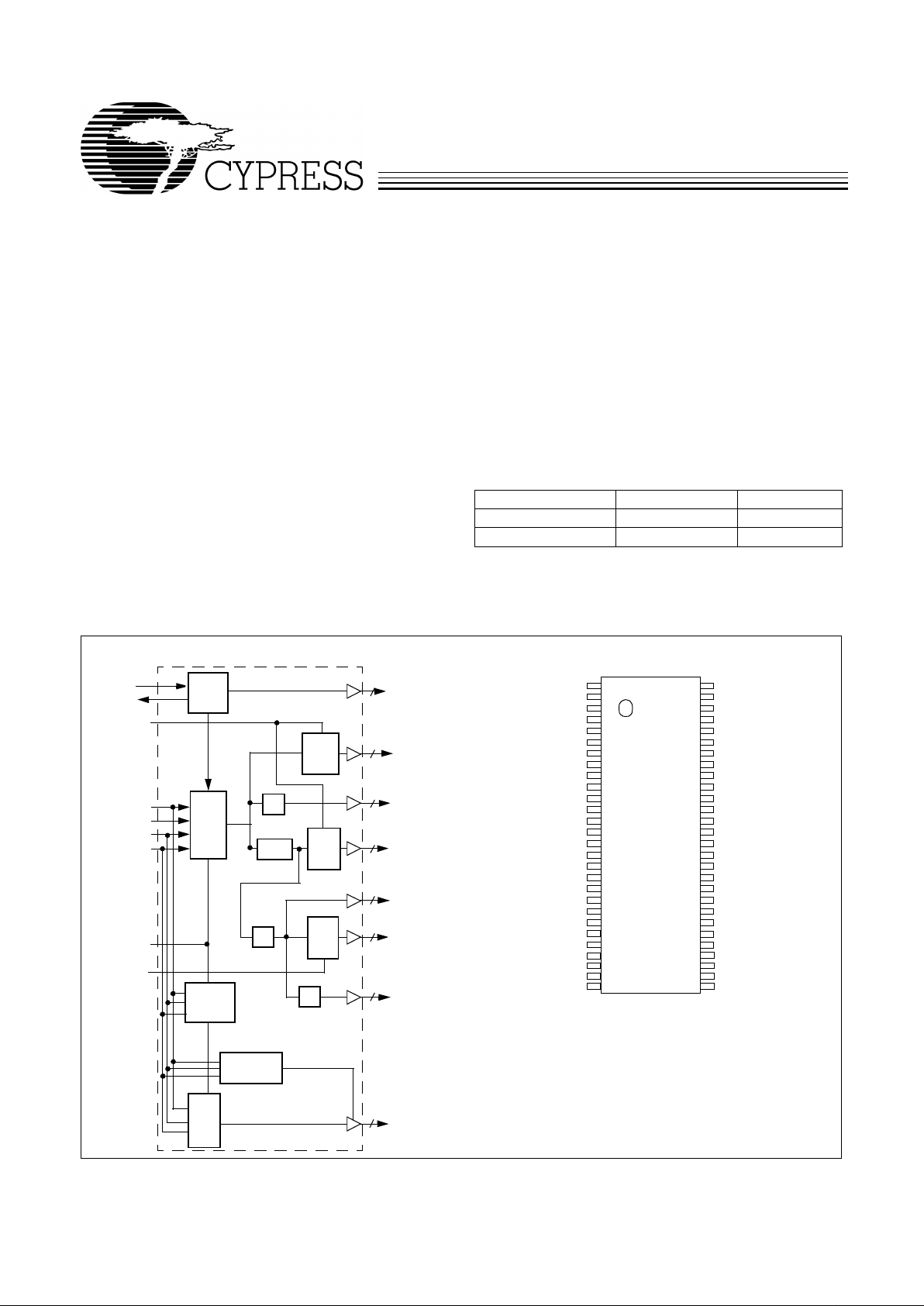
Block Diagram
Pin Configuration
REF0:1
CPU0:3
CPUdiv2_0:1
3V66_0:3
XTAL
PLL 1
SPREAD#
X2
X1
PCI_F
PCI1:7
IOAPIC0:2
48MHz
PLL2
OSC
÷2
STOP
Logic
Power
Three-state
Logic
SEL0
SEL1
SEL133/100#
Clock
CPU_STOP#
÷2/÷1.5
STOP
Logic
Clock
Down
Logic
÷2
STOP
Logic
Clock
÷2
2
4
2
4
1
7
3
1
PCI_STOP#
PWRDWN#
GND
REF0
REF1
VDDQ3
X1
X2
GND
PCI_F
PCI1
VDDQ3
PCI2
PCI3
GND
PCI4
PCI5
VDDQ3
PCI6
PCI7
GND
GND
3V66_0
3V66_1
VDDQ3
GND
W133
VDDQ2
IOAPIC2
IOAPIC1
IOAPIC0
GND
VDDQ2
CPUdiv2_1
CPUdiv2_0
GND
VDDQ2
CPU3
CPU2
GND
VDDQ2
CPU1
CPU0
GND
VDDQ3
GND
PCI_STOP#
CPU_STOP#
PWRDWN#
SPREAD#
SEL1
56
55
54
53
52
51
50
49
48
47
46
45
44
43
42
41
40
39
38
37
36
35
34
33
1
2
3
4
5
6
7
8
9
10
11
12
13
14
15
16
17
18
19
20
21
22
23
24
25
26
27
28
32
31
30
29
3V66_2
3V66_3
VDDQ3
SEL133/100#
SEL0
VDDQ3
48MHz
GND
Page 2
W133
PRELIMINARY
2
Overview
The W133 is designed to provide the essential frequency
sources to work with advanced multiprocessing Intel® arch itecture pl atforms. Spl it voltage supply signaling provides 2.5V
and 3.3V clock f requencies operati ng up to 133 MHz.
From a low-cost 14.31818-MHz reference crystal oscillator,
the W133 generates 2.5V clock outputs to sup port CPUs, core
logic chip set , and Direct RDRAM cloc k gener ators. It also provides skew-controlled PCI and IOAPIC cl ocks synchronous to
CPU clock, 48- MHz Universal Serial Bus (USB) clock, and replicates the 14.31818-MHz reference clock.
All CPU, PCI, and IOAPIC clocks c an be synchronously modulated for spread spectrum operations. Cypress employs proprietary techniques that provide the maximum EMI reduction
while minimizing the clock skews that could reduce system
timing margins. Spread Spectrum modulation is enabled by
the active LOW control signal SPREAD#.
The W133 also includes po wer management contro l inputs. By
using these inputs, system logic can stop CPU and/or PCI
clocks or power down the entire device to conserve system
power.
Pin Definitions
Pin Name Pin No.
Pin
Type Pin Description
CPU0:3 41, 42, 45, 46 O
CPU Clock Outputs 0 through 3:
These fo ur CPU cloc k s run at a f requ ency set b y
SEL133/100#. Output voltage swin g is set by the voltage applied to VDDQ2.
CPUdiv2_ 0:1 49,50 O
Synchronous M emory Refere nce Clock Out put 0 thr ough 1:
Reference clock f or
Direct RDRAM clock genera tors running at 1/2 CPU clock frequency. Output voltage
swing is set by the voltage applied to VDDQ2.
PCI1:7 9, 11 , 12, 14, 1 5,
17, 18
O
PCI Clock Outputs 1 t hrough 7:
These se ven PCI cloc k outp uts run sy nchronously
to the CPU clock. Voltage swing is set by the power connection to VDDQ3. PCI1:7
outputs are stopped when PCI _STOP# is held LOW .
PCI_F 8 O
PCI_F (PCI Free-running):
This PCI clock output runs synchronously to the CPU
clock. V oltag e swing is set by the power connection to VDDQ3. PCI_F is n ot affe cted
by the state of PCI_STOP#.
REF0:1 2, 3 O
14.318-MHz Reference Cloc k Output:
3.3V copies of the 14.318-MHz reference
clock.
IOAPIC0:2 53, 54, 55 O
I/O APIC Clock Output:
Provides 16.67 -MHz fixed frequenc y. The output voltage
swing is set by the power connection to VDDQ2.
48MHz 30 O
48-MHz O u tp u t:
Fixed 48-MHz USB output. Output voltage swing is controlled by
voltage app li ed to VDDQ3.
3V66_0:3 21, 22, 25, 26 O
66-MHz Output 0 through 3:
Fixed 66-MHz outputs. Output voltage swing is con-
trolled by voltage applied to VDDQ3.
SEL0:1 32, 33 I
Mode Select Input 0 through 1:
3.3V LVTTL-compatible input for selecting clock
output modes.
SEL133/100# 28 I
Frequency Selecti on Input:
3.3V L VTTL-c ompatibl e input that selects CPU output
frequency as shown in Tabl e 1.
X1 5 I
Crystal Connection or External Reference Frequency Input:
Connect to either
a 14.318-MHz crystal or an external refer ence signal.
X2 6 O
Crystal Connection:
An output connection for an external 14.318-MHz crystal. If
using an external reference, this pin must be left unconnected.
SPREAD# 34 I
Active LO W Spread Spectrum Enabl e:
3.3V L VTTL- compatib le input t hat enabl es
spre ad spec t rum m o de when held L OW.
PWRDWN# 35 I
Active LOW Power Down Input:
3.3V LVTTL-compatible asynchronous input that
requests the de vice to enter power-down mode.
CPU_STOP# 36 I
Active LOW CPU Clock Stop:
3.3V LVTTL-compatible asynchronous input that
stops all CPU and 3V66 cloc ks when held LO W . CPUdiv2 output s are unaff ected by
this input.
PCI_STOP# 37 I
Active LOW PCI Cloc k Stop:
3.3V LVTTL-compatible asynchr onous input that
stops all PCI outputs except PCI_F when held LOW.
VDDQ3 4, 10, 16, 23, 27,
31, 39
P
Power Connection:
Power suppl y for PCI output buff ers, 48-MHz USB output buff er,
Reference output buff ers, 3V66 outpu t buffers , core logic, and PLL ci rcuitry . Connect
to 3.3V supply.
VDDQ2 43, 47, 51, 56 P
Power Connection:
Power supply for IOAPIC, CPU, and CPUdiv2 output buffers.
Connect to 2.5V supply.
GND 1, 7, 13, 19, 20,
24, 29, 38, 40,
44, 48, 52
G
Ground Connecti on:
Connect all ground pin s to the common s ystem gr ound plane .
Page 3
W133
PRELIMINARY
3
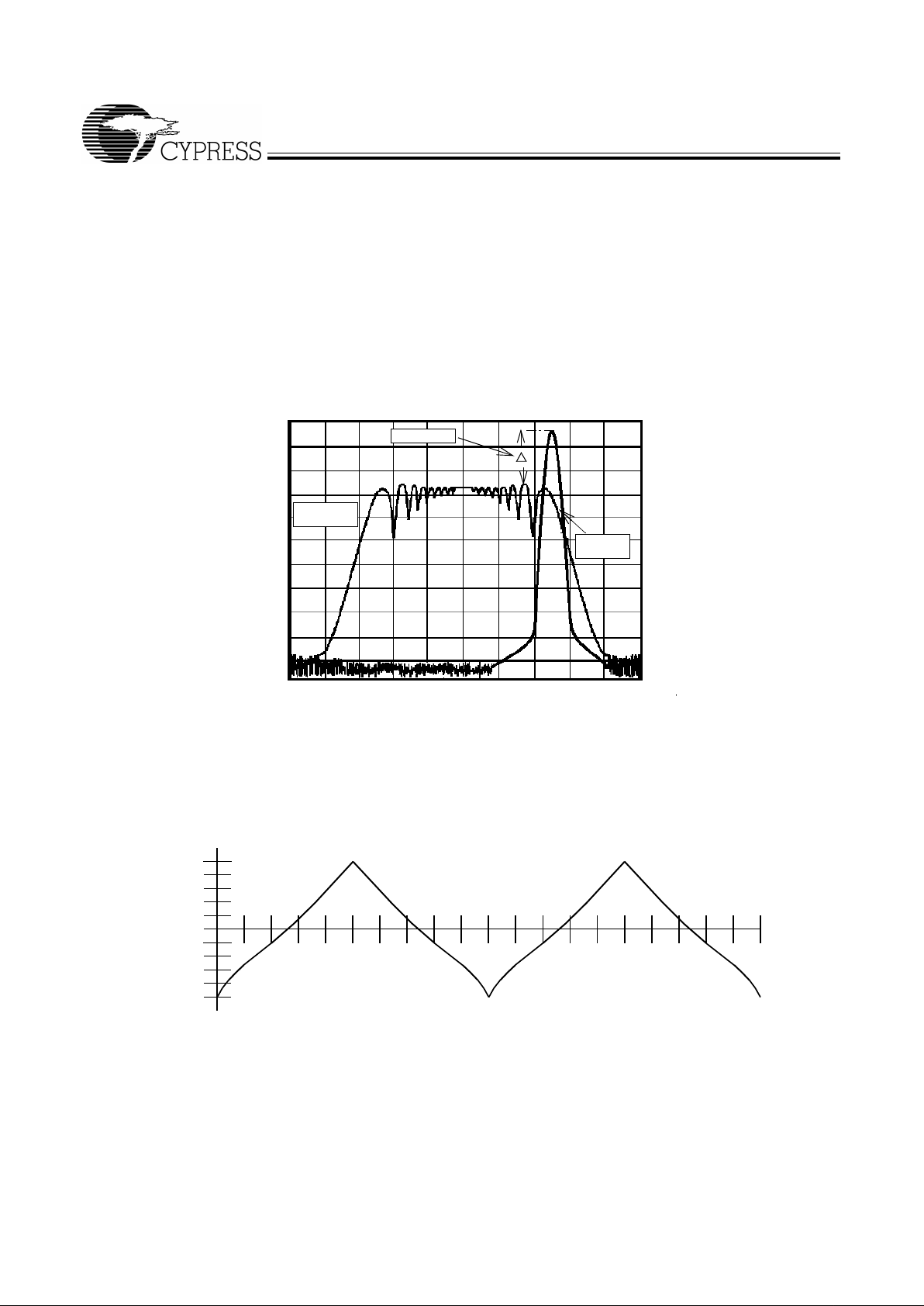
Spread Sp ectrum C locki n g
The device gener ates a clock that is frequency modulated in
order to increase the bandwidth that it occu pies. By increas ing
the bandwidth of the fundamental and its harmonics, the amplitudes of the radiated electromagnetic emissions are reduced. This effect is depicted in Figure 1.
As shown in Figure 1, a harmonic of a modulated clock has a
much low er amplitude th an that of an un modulated si gnal. The
reduction in amplitude is dependent on the harmonic number
and the frequency deviation or spread. The equation for the
reduction is
dB = 6.5 + 9*log
10
(P) + 9*log10(F)
Where P is the percentage of deviation and F is the frequency
in MHz where the reduction is measured.
The output clock is modulated with a waveform depicted in
Figure 2. This waveform, as discussed in “Spread Spect rum
Clock Generation f or the Reducti on of Radiated Emissio ns” by
Bush, Fessler, and Hardin produces the maximum reduction
in the amplitude of radiated elect romagnetic emissions. The
deviati on selec ted for this chip i s –0.5% do wnspr ead. Fi gure 2
details the Cypress spr eading pat tern. Cypress does offer options with more spread and greater EMI reduction. Cont act
your local Sales representative for details on these devices .
Spread
Spectrum
Enabled
EMI Reduction
Spread
Spectrum
Non-
Figure 1. Typical Clock and SSFTG Comparison
100%
60%
20%
80%
40%
0%
–20%
–40%
–60%
–80%
–100%
10%
20%
30%
40%
50%
60%
70%
80%
90%
100%
10%
20%
30%
40%
50%
60%
70%
80%
90%
100%
Time
Frequency Shift
Figure 2. Modulation W aveform Profile
Page 4
W133
PRELIMINARY
4
Mode Selection Functions
The W133 supports the following operating mo des controlled through the SEL133/100#, SEL0, and SEL1 inputs.
Notes:
2. Provided for board level “bed of nails” testing.
3. 48-MHz PLL disabled to reduce component jitter.
4. “Normal” mode of operation.
5. TCLK is a test clock over driven on the X1 input during test mode. TCLK mode is based on 133-MHz CPU select logic.
6. Required for DC output impedance verification.
7. Range of reference frequency is min.=14.316, nominal = 14.31818 MHz, max.=14.32 MHz.
8. Frequency accuracy of 48 MHz is +167 PPM to match USB default.
Table 2. Select Functions
SEL133/100# SEL1 SEL0 Function
0 0 0 All Outputs Three-State
00 1(Reserved)
0 1 0 Active 100 MHz, 48 MHz PLL Inactive
0 1 1 Active 100 MHz, 48 MHz PLL Active
1 0 0 Test Mode
10 1(Reserved)
1 1 0 Active 133 MHz, 48 MHz PLL Inactive
1 1 1 Active 133 MHz, 48 MHz PLL Active
Table 3. Truth Table
SEL
133/100# SEL1 SEL0 CPU CPUdiv2 3V66 PCI 48MHz REF IOAPIC Notes
0 0 0 HI-Z HI-Z HI-Z HI-Z HI-Z HI-Z HI-Z 2
0 0 1 n/a n/a n/a n/a n/a n/a n/a
0 1 0 100 MHz 50 MHz 66 MHz 33 MHz HI-Z 14.318 MHz 16.67 MHz 3
0 1 1 100 MHz 50 MHz 66 MHz 33 MHz 48 MHz 14.318 MHz 16.67 MHz 4, 7, 8
1 0 0 TCLK/2 TCLK/4 TCLK/4 TCLK/8 TCLK/2 TCLK TCLK16 5, 6
1 0 1 n/a n/a n/a n/a n/a n/a n/a
1 1 0 133 MHz 66 MHz 66 MHz 33 MHz HI-Z 14.318 MHz 16.67 MHz 3
1 1 1 133 MHz 66 MHz 66 MHz 33 MHz 48 MHz 14.318 MHz 16.67 MHz 4, 7, 8
Table 4. Maximum Supply Current
Condition
Max. 2.5V supply consumption
Max. discrete cap loads,
V
DDQ2
=2.625V
All static inputs=V
DDQ3
or GN D
Max. 3.3V supply consumption
Max. discrete cap loads,
V
DDQ3
=3.465V or GND
Powerdown Mode
(PWRDWN#=0)
100 µA 200 µA
FUll Active 100MHz
SEL133/100#=0
SEL1, 0=11
CPU_STOP#, PCI_STOP#=1
75 mA 160 mA
Full Active 133MHz
SEL133/100#=0
SEL1, 0=11
CPU_STOP#, PCI_STOP#=1
90 mA 160 mA
Page 5

W133
PRELIMINARY
5
T able 5. Clock Enable Configuration
[9, 10, 11 , 12, 13, 14]
CPU_STOP# PWRDWN# PCI_STOP# CPU CPUdiv2 IOAPIC 3V66 PCI PCI_F
REF,
48MHz OSC. VCOs
X 0 X LOW LOW LOW LOW LOW LOW LOW OFF OFF
0 1 0 LOW ON ON LOW LOW ON ON ON ON
0 1 1 LOW ON ON LOW ON ON ON ON ON
1 1 0 ON ON ON ON LOW ON ON ON ON
111ONONONONONONONONON
Table 6. Power Management State Transition
[15, 16]
Signal Signal State
Latency
No. of rising edges of PCI Clock
CPU_STOP# 0 (disabled) 1
1 (enabled) 1
PCI_STOP# 0 (disabled) 1
1 (enabled) 1
PWRDWN# 1 (normal operati on) 3 ms
0 (power down) 2 max.
Timing Diagrams
CPU_STOP# Timing Dia gram
[17, 18, 19 , 20, 21, 22]
Notes:
9. LOW means outputs held static LOW as per latency requirement below.
10. ON means active.
11. PWRDWN# pulled LOW, impacts all outputs including REF and 48-MHz outputs.
12. All 3V66 as well as all CPU clocks stop cleanly when CPU_STOP# is pulled LOW.
13. CPUdiv2, IOAPIC, REF, 48MHz signals are not controlled by the CPU_STOP# functionality and are enabled in all conditions except PWRDWN#=LOW.
14. An “x” indicates a “don’t care” condition.
15. Clock on/off latency is defined in the number of rising edges of the free-running PCI clock between when the clock disable goes LOW/HIGH to when the first
valid clock comes out of the device.
16. Power up latency is from when PWRDWN# goes inactive (HIGH) to when the first valid clocks are driven from the device.
17. All internal timing is referenced to the CPU clock.
18. The internal label means inside the chip and is a reference only. This in fact may not be the way that the control is designed.
19. CPU_STOP# signal is an input signal that must be made synchronous to free-running PCI_F.
20. 3V66 clocks also stop/start before.
21. PWRDWN# and PCI_STOP# are shown in a HIGH state.
22. Diagrams shown with respect to 133 MHz. Similar operation when CPU clock is 100 MHz.
CPU
PCI
CPU_STOP#
PCI_STOP#
PWRDWN#
3V66
(internal)
HI
HI
CPU
(external)
Page 6

W133
PRELIMINARY
6
PCI_STOP# Timing Diagram
[17, 18, 22, 23, 24, 25]
PWRDWN# Timing Diagram
[17, 22, 26 , 27]
Notes:
23. PCI_STOP# signal is an input signal that must be made synchronous to PCI_F output.
24. All other clocks continue to run undisturbed.
25. PWRDWN# and CPU_STOP# are shown in a HIGH state.
26. The internal label means inside the chip and is a reference only. This in fact may not be the way that the control is designed.
27. PWRDWN is an asynchronous input and metastable conditions could exist. This signal is required to be synchronized.
28. The shaded sections on the VCO and the Crystal signals indicate an active clock.
Timing Diagrams
(continued)
CPU
PCI
PCI_STOP#
PWRDWN#
PCI_F
(external)
HI
HI
(internal)
PCI
(external)
CPU_STOP#
CPU
PCI
PWRDWN#
VCO
Crystal
PCI
CPU
(internal)
(internal)
(external)
(external)
Page 7

W133
PRELIMINARY
7
Absolute Maximum Ratings
Stresses gre ater th an those list ed i n this tab le may cause permanent damage to the de vice. These represent a str ess ratin g
only. Operation of the device at these or any other conditions
above those specified in the operatin g sections of this specification is not implied. Maximum conditions for extended periods may affect reliability .
.
Parameter Description Rating Unit
V
DD
, V
IN
V oltage on any pin with respect to GND –0.5 to +7 .0 V
T
STG
Storage Temperature –65 to +150 °C
T
A
Operating Temperature 0 to +70 °C
T
B
Ambient Temperature under Bias –55 to +125 °C
ESD
PROT
Input ESD Protection 2 (min.) kV
DC Electr i cal C h ar acteristi cs:
TA = 0°C to +70°C, V
DDQ3
= 3.3V±5%, V
DDQ2
= 2.5V±5%
Parameter Description Tes t Condi ti on Min. Typ. Max. Unit
Supply Current
I
DD-3.3V
Combined 3.3V Supply Current CPU0:3 =133 MHz
[29]
160 mA
I
DD-2.5
Combined 2.5V Supply Current CPU0:3 =133 MHz
[29]
90 mA
Logic Inputs (All referenced to V
DDQ3
= 3.3V)
V
IL
Input Low V oltage GND –
0.3
0.8 V
V
IH
Input High V oltage 2.0 V
DD
+ 0.3 V
I
IL
Input Low Current
[30]
–25 µA
I
IH
Input High Current
[30]
10 µA
I
IL
Input Low Current, SEL133/100#
[30]
–5µA
I
IH
Input High Current, SEL133/100#
[30]
5µA
Clock Outputs
CPU, CPUdiv2, IO APIC (Referenced to V
DDQ2
) Test Condition Min. Typ. Max. Unit
V
OL
Output Low Voltage IOL = 1 mA 50 mV
V
OH
Output High Voltage IOH = –1 mA 2.2 V
I
OL
Output Low Current V
OL
= 1.25V 45 65 100 mA
I
OH
Output High Current VOH = 1.25V 45 65 100 mA
48MHz, REF (Refere n ce d to V
DDQ3
) Test Condition Min. T yp. Max. Unit
V
OL
Output Low Voltage IOL = 1 mA 50 mV
V
OH
Output High Voltage I
OH
= –1 mA 3.1 V
I
OL
Output Low Current V
OL
= 1.5V 45 65 100 mA
I
OH
Output High Current V
OH
= 1.5V 45 65 100 mA
PCI, 3V66 (Referenced to V
DDQ3
) Tes t Condi tion Min. Typ. Max. Unit
V
OL
Output Low Voltage I
OL
= 1 mA 50 mV
V
OH
Output High Voltage IOH = –1 mA 3.1 V
I
OL
Output Low Current VOL = 1.5V 70 100 145 mA
I
OH
Output High Current V
OH
= 1.5V 65 95 135 mA
Notes:
29. All clock outputs loaded with 6" 60Ω transmission lines with 20-pF capacitors.
30. W133 logic inputs have internal pull-up devices, except SEL133/100# (pull-ups not CMOS level).
Page 8

W133
PRELIMINARY
8
3.3V AC Electri cal C h ar acteristi cs
T
A
= 0°C to +70°C, V
DDQ3
= 3.3V±5%,V
DDQ2
= 2.5V± 5%, f
XTL
= 14.31818 MHz
Spread Spectrum functi on turned off
AC clock parameters are tested and guaranteed over st ated operating conditions using the stat ed lump capacitive load at the
clock o utput.
[34]
Notes:
31. X1 input threshold voltage (typical) is V
DD
/2.
32. The W133 contains an internal crystal load capacitor between pin X1 and ground and another between pin X2 and ground. Total load placed on crystal is 18 pF;
this includes typical stray capacitance of short PCB traces to crystal.
33. X1 input capacitance is applicable when driving X1 with an external clock source (X2 is left unconnected).
34. Period, jitter, offset, and skew measured on rising edge at 1.5V.
35. 3V66 is CPU/2 for CPU =133 MHz and (2 x CPU)/3 for CPU = 100 MHz.
Crystal Oscillator
V
TH
X1 Input threshold Voltage
[31]
1.65 V
C
LOAD
Load Capacitance, Imposed on
External C rys tal
[32]
18 pF
C
IN,X1
X1 Input Capacitance
[33]
Pin X2 unconnected 28 pF
Pin Capacitance/Induct ance
C
IN
Input Pin Capacitance Except X1 and X2 5 pF
C
OUT
Output Pin Capacitance 6 pF
L
IN
Input Pin Inductance 7nH
DC Electr i cal C h ar acteristi cs:
TA = 0°C to +70°C, V
DDQ3
= 3.3V±5%, V
DDQ2
= 2.5V±5% (continued)
Parameter Description Tes t Condi ti on Min. Typ. Max. Unit
3V66 Clock Outputs, 3V66_0:3 (Lump Capacitance Test Load = 30 pF)
Parameter Description Test Condi ti on/Comments Min. Typ. Max. Unit
f Frequency Note 35 66.6 MHz
t
R
Output Rise Edge Rate Measured from 0.4V to 2.4V 1 4 V/ns
t
F
Output Fall Edge Rate Measured from 2.4V to 0.4V 1 4 V/ns
t
D
Duty Cycle Measu red on rising and falling edge at 1.5V 45 55 %
f
ST
Frequency Stabilization
from Power-up (cold start)
Assumes full su pply voltage reached within
1 ms from power-up. Short cycles exist prior
to frequency stabilization.
3ms
Z
o
AC Output Impe dance A verage value during switching transition.
Used for determining series termination
value.
15 Ω
Page 9

W133
PRELIMINARY
9
Note:
36. PCI clock is CPU/4 for CPU = 133 MHz and CPU/3 for CPU = 100 MHz.
PCI Clock Outputs, PCI_F and PCI1:7 (L ump Capacit ance Test Load = 30 pF)
Parameter Description Test Condit ion/Comments Min. Typ. Max. Unit
t
P
Period Measured on rising edge at 1.5V
[36]
30 ns
t
H
High Time Duration of clock cycle above 2.4V 12 ns
t
L
Low Time Duration of clock cyc le below 0.4V 12 ns
t
R
Output Rise Edge Rate Measured from 0.4V to 2.4V 1 4 V/ns
t
F
Output Fall Edge Rate Measured from 2.4V to 0.4V 1 4 V/ns
t
D
Duty Cycle Measured on rising and falling edge at 1.5V 45 55 %
t
JC
Jitter, Cycle-to-Cycle Measured on rising edge at 1.5V. Maximum di fference of
cycle time between two adjacent cycles.
500 ps
t
SK
Output Skew Measured on risi ng edge at 1.5V. 500 ps
t
O
3V66 to PCI Clock
Skew
Covers all 3V66/PCI outputs. Measu red on rising edge at
1.5V. 3V66 leads PCI output.
1.5 4 ns
f
ST
Frequenc y Stabilization
from Power-up (cold
start)
Assumes full supply voltage reached within 1 ms from
power-up . Short cycles e xist prior t o frequency st abilization.
3ms
Z
o
AC Output Impe dance Average val ue duri ng switching transition. Used for deter-
mining series termination value.
15 Ω
REF Clock Outputs, REF0:1 (Lump Capaci tance Test Load = 20 pF)
Parameter Description Test Condition/Comments Min. Typ. Max. Unit
f Frequency, Actual Frequency generated by crystal oscillator 14.318
t
R
Output Rise Edge Rate Measured from 0.4V to 2.4V 0.5 2 V/ns
t
F
Output Fall Edge Rate Measured from 2.4V to 0.4V 0.5 2 V/ns
t
D
Duty Cycle Measured on rising and falling edge at 1.5V 45 55 %
f
ST
Frequency St abilization from
Power-up (cold start)
Assumes full supply voltage reached within
1 ms from power-up. Short cycles exist prior to
frequency stabi li zation.
3ms
Z
o
AC Output Impedance Ave rage value during s witching tr ansition. Used
for determining seri es termination value.
25 Ω
48-MHZ Clock Output (Lump Capac it ance Test Load = 20 pF)
Parameter Description Test Condition/Comments Min. Typ. Max. Unit
f F requency, Actual Determined by PLL divider ratio (see m/n below) 48.008 MHz
f
D
Deviation from 48 MHz (48.008 – 48)/48 +167 ppm
m/n PLL Rati o (14.31818 MHz x 57/17 = 48.008 MHz) 57/17
t
R
Output Rise Edge Rate Measured from 0.4V to 2.4V 0.5 2 V/ns
t
F
Output Fall Edge Rate Measured from 2.4V to 0.4V 0.5 2 V/ns
t
D
Duty Cycle M easured on rising and falling edge at 1.5V 45 55 %
f
ST
Frequency Stabilization
from Power-up (cold start)
Assumes full supply vol tage reached withi n 1 ms
from power-up. Short cycles exist prior to frequency stabilization.
3ms
Z
o
AC Output Impedance Average value during switching transition. Used
for determining seri es termi nation value.
25 Ω
Page 10

W133
PRELIMINARY
10
2.5V AC Electri cal C h ar acteristi cs
T
A
= 0°C to +70°C, V
DDQ3
= 3.3V±5%, V
DDQ2
= 2.5V±5%
f
XTL
= 14.31818 MHz
Spread Spectrum functi on turned off
AC clock parameters are tested and guaranteed over st ated operating conditions using the stat ed lump capacitive load at the
clock o utput.
[37]
Note:
37. Period, Jitter, offset, and skew measured on rising edge at 1.25V.
CPU Clock Outputs, CPU0:3 (Lump Capacitance Test Load = 20 pF)
Parameter Description Test Condition/Comments
CPU = 133MHz CPU = 100MHz
UnitMin. Typ. Max. Min. Typ. Max.
t
P
Period Measured on rising edge at 1. 25V 7.5 7.65 10 10.2 ns
t
H
High Time Duration of clock cycle above 2.0V 1.87 3.0 ns
t
L
Low Time Duration of clock cycle below 0. 4V 1.67 2.8 ns
t
R
Output Rise Edge Rate Measured from 0.4V to 2.0V 1 4 1 4 V/ns
t
F
Output Fall Edge Rate Measured from 2.0V to 0.4V 1 4 1 4 V/ns
t
D
Duty Cycle M easured on rising and falling edge at
1.25V
45 55 45 55 %
t
JC
Jitter , Cycle-to-Cycle Measured on rising edge at 1.25V. Max-
imum differ ence of cycle time between
two adjacent cycles.
250 250 ps
t
SK
Output Skew Measured on rising edge at 1.25V 175 175 ps
f
ST
Frequency Stabilization from Po wer-up
(cold start)
Assumes full supply voltage reached
within 1 ms from power-up . Short cycles
exist prior to frequency stabilization.
33ms
Z
o
AC Output Impedance Average value during switching transi-
tion. Used for dete rmini ng series terminat i o n value.
20 20 Ω
CPUdiv2 Clock Outputs, CPUdiv 2_0:1 (Lump Capacitance Test Load = 20 pF)
Parameter Description Test Condition/Comments
CPU = 133 MHz CPU = 100 MHz
UnitMin. Typ. Max. Min. Typ. Max.
t
P
Period Measured on rising edge at 1.25V 15 15.3 20 20.4 ns
t
H
High Time Duration of clock cycle above 2.0V 5.25 7.5 ns
t
L
Low Time Duration of clock cycle below 0.4V 5.05 7.3 ns
t
R
Output Rise Ed ge Rate Measured from 0.4V to 2.0V 1 4 1 4 V/ns
t
F
Output Fall Edge Rate Measured from 2.0V to 0.4V 1 4 1 4 V/ns
t
D
Duty Cycle Measured on rising and falling edge at
1.25V
45 55 45 55 %
t
JC
Jitter , Cycle-to-Cycle Measured on rising edge a t 1.2 5V. Max-
imum difference of cycle time between
two adjacent cycles.
250 250 ps
t
SK
Output Skew Measured on rising edge at 1.25V 175 175 ps
f
ST
Frequency Stabilization from Po wer-up
(cold start)
Assumes full suppl y voltage reached
within 1 ms from pow er-up. Short cycles
exist prior to frequency stabilization.
33ms
Z
o
AC Output Impeda nce Av erage value during sw itching transi-
tion. Used for determining series termination val ue.
20 20 Ω
Page 11

W133
PRELIMINARY
11
Note:
38. IOAPIC clock is CPU/8 for CPU = 133 MHz and CPU/6 for CPU = 100 MHz.
Intel is a registered trademark of Intel Corporation.
Document #: 38-00823
IOAPIC Clock Outputs, IOAPIC0:2 (Lump Capacitance Test Load = 20 pF)
Parameter Description Test Condition/Comments Min Typ Max Unit
f Frequency Note 38 16.67 MHz
t
R
Output Rise Edge Rate Measured from 0.4V to 2.0V 1 4 V/ns
t
F
Output Fal l Edge Rate Measured from 2.0V to 0.4V 1 4 V/ns
t
D
Duty Cycle M easured on rising and falling edge at 1.25V 45 55 %
f
ST
Frequency Stabilization
from Power-up (cold start)
Assumes full supply voltage reached within
1 ms from power-up . Sh ort cycles exist prior to
frequency stabi li zation.
3ms
Z
o
AC Output Impedance Avera ge value during swit ching transition. Used
for determining seri es termi nation value.
20 Ω
Ordering Information
Ordering Code
Package
Name Package Type
W133 H 56-pin SSOP (300 mils)
Page 12

W133
PRELIMINARY
© Cypress Semiconductor Corporation, 1999. The information contained herein is subject to change without notice. Cypress Semiconductor Corporation assumes no responsibility for the use
of any circuitry other than circuitry embodied in a Cypress Semiconductor product. Nor does it con vey or imply any license under patent or other rights. Cypress Semiconductor does not authorize
its products for use as critical components in life-support systems where a malfunction or failure may reasonably be expected to result in significant injury to the user. The inclusion of Cypress
Semiconductor products in life-support systems application implies that the manufacturer assumes all risk of such use and in doing so indemnifies Cypress Semiconductor against all charges.
Package Diagram
56-Pin Small Shrink Outlin e P ackage (SSOP, 300 mils)
Summary of nominal dimensions in i nches:
Body Width: 0.296
Lead Pitch: 0.025
Body Length: 0.625
Body Height: 0.102
 Loading...