

Page 1

Hyperabrupt Varactor-Tuned
GROUND
CASE GROUND
+DC
VOLTAGE
RF OUT
+V
3
1
24
TUNE
Oscillators
Technical Data
VTO-9000 Series
Features
• 25 MHz to 2.3 GHz Coverage
• Fast Tuning
• Fast Setting Time
• +20 VDC Max Tuning
Voltage
• 10 mW Output Power
• ± 2.0 dB Output Flatness
• Hermetic Thin-film
Construction
Description
HP VTO-9000 Hyperabrupt Series
oscillators use a silicon transistor
chip as a negative resistance
oscillator. The oscillation frequency is determined by a silicon
hyperabrupt varactor diode acting
as a voltage-variable capacitor in a
thin-film microstripline resonator.
Schematic
Series Feedback
+15 V
This provides extremely fast
tuning speed limited primarily by
the internal impedance of the
user-supplied voltage driver.
This family of oscillators is
similar to the standard commercial VTO-8000 Series except for
the incorporation of a silicon
hyperabrupt varactor tuning
diode. This enables the oscillator
to be tuned over the specified
range in less than 20 volts rather
than 40 to 50␣ volts in conventional oscillators.
The VTO-9000 Series VTOs are
packaged in TO-8 transistor cans
for simple installation in a
conventional 50-ohm
microstripline PC board. They
are ideal for most compact
RF OutputOutput Matching
Pin Configuration
TO-8V
lightweight commercial and
military equipment designs.
Test fixturing is also available for
lab bench test applications. See
the “Test Fixtures for TO-8
Packages” section for additional
information and outlines.
Applications
The VTO-9000 Series oscillators
may be used in the same applications as VTO-8000 Series oscillators. The VTO-9000 Series is the
desired choice for superior
linearity and modulation sensitivity requirements.
Varactor
V Tune
5964-9814E
Capacitor
Tuning
Port
Resonator
9-30
Page 2

Electrical and Performance Specifications
Guaranteed Specifications @ 25°C Case Temperature (0° to +65° C Operating Temperature)
Model No. VTO–9032 VTO–9050 VTO–9068 VTO–9090
Frequency Range, Min. 320–640 MHz 500–1000 MHz 680–1360 MHz, 900–1600 MHz
Power Output Into 50–ohm Load, Min . 10 mW/+10 dBm 10 mW/+ 10 dBm 10 mW/+10 d Bm 10 mW/+10 dBm
Power Output Variation @ 25°C, Max. ± 2 dB ± 2 dB ± 2 dB ± 2 dB
Operating Carrier Temperature Range 0° to +65°C0° to +65°C0° to +65° C0° to +65°C
Frequency Drift Over Operating Temperature, Typ. 12 MHz 20 MHz 20 MHz 20 MHz
Pulling Figure (12 dB Return Loss), Typ. 20 MHz 20 MHz 25 MHz 25 MHz
Pushing Figure, +15 VDC Supply, Typ. 5 MHz/V 5 MHz/V 6 MHz/V 6 MHz/V
Harmonics, Below Carrier, Typ. –14 dB –10 dB –14 dB –14 dB
Spurious Output Below Carrier, Min. –60 dB –60 dB –60 dB –60 dB
Tuning Voltage
Low Frequency, Min. 0 VDC 0 VDC 0 VDC 2 VDC
High Frequency, Max 20 VDC 20 VDC 20 VDC 18 VDC
Maximum Tuning Voltage +20 VDC +20 VDC +20 VDC +20 VDC
Tuning Port Capacitance, Nom. 200 pF 200 pF 190 pF 190 pF
Phase Noise, Single Sideband,
1 Hz Bandwidth, Typ.
50 kHz From Carrier –95 dBc/Hz –100 dBc/Hz –95 dBc/Hz –100 dBc/Hz
100 kHz From Carrier –103 dBc/Hz –108 dBc/Hz –103 dBc/Hz –108 dBc/Hz
Input Power, ± 1% Regulaltion
Voltage, Nom. +15 VDC +15 VDC +15 VDC +15 VDC
Current, Max. 50 mA 50 mA 50 mA 50 mA
Case Style TO–8V TO–8V TO–8V TO–8V
Electrical and Performance Specifications
Guaranteed Specifications @ 25°C Case Temperature (0° to +65° C Operating Temperature)
Model No. VTO–9120 VTO–9130
Frequency Range, Min. 1200–2000 MHz 1300–2300 MHz
Power Output Into 50–ohm load, Min. 10 mW/+10 dBm 10 mW/+10 dBm
Power Output Variation @ 25°C, Max. ± 2 dB ± 1.5 dB
Operating Case Temperature Range 0° to +65° C0° to +65°C
Frequency Drift Over Operating Temperature, Typ. 25 MHz 25 MHz
Pulling Figure (12 dB Return Loss), Typ. 25 MHz 50 MHz
Pushing Figure, +15 VDC Supply, Typ. 10 MHz/V 10 MHz/V
Harmonics, Below Carrier, Typ. –14 dB –15 dB
Spurious Output Below Carrier, Min. –60 dB –60 dB
Tuning Voltage
Low Frequency 3±1 VDC 2 VDC Min.
High Frequency 12± 2 VDC 20 VDC Max.
Maximum Tuning Voltage +20 VDC + 20 V DC
Tuning Port Capacitance, Nom. 100 pF 100 pF
Phase Noise, Single Sideband,
1 Hz, Bandwidth, Typ.
50 kHz From Carrier –97 dBc/Hz –97 dBc/Hz
100 kHz From Carrier –105 dBc/Hz –105 dBc/Hz
Input Power, ± 1% Regulation
Voltage,Nom. +15VDC +15VDC
Current, Max. 50 mA 50 mA
Case Style TO–8V TO–8V
9-31
Page 3
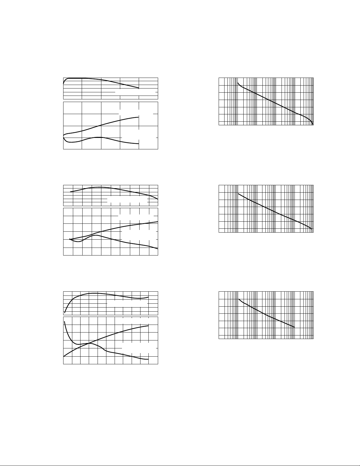
Typical Performance @ 25ºC Case Temperature
17
15
13
POWER
11
1000
OUTPUT, dBm
500
MHz
FREQUENCY,
0
0
5 10152025
TUNING VOLTAGE, VDC
Figure 1. VTO-9032 Power Output, Frequency
and Modulation Sensitivity vs. Tuning Voltage
POWER OUTPUT
TUNING CURVE
MODULATION
SENSITIVITY
100
MODULATION
SENSITIVITY, MHz/V
0
–40
–60
–80
–100
–120
–140
LOG £(f), dBc/Hz
–160
1K 10K 100K 1M 10M
FOURIER FREQUENCY, Hz
Figure 2. VTO-9032 Normalized Phase Noise
@ 640 MHz S.S.B. Power Spectral Density.
16
14
12
POWER
10
1500
OUTPUT, dBm
1000
MHz
500
FREQUENCY,
0
0
2468 20
TUNING VOLTAGE, VDC
POWER OUTPUT
TUNING CURVE
MODULATION
SENSITIVITY
10 12 14 16 18
Figure 3. VTO-9050 Power Output, Frequency
and Modulation Sensitivity vs. Tuning Voltage.
11
10
9
8
POWER
7
OUTPUT, dBm
1374
1178
962
MHz
786
FREQUENCY,
590
0
2468 20
TUNING VOLTAGE, VDC
POWER OUTPUT
TUNING CURVE
MODULATION
SENSITIVITY
10 12 14 16 18
Figure 5. VTO-9068 Power Output, Frequency and
Modulation Sensitivity vs. Tuning Voltage.
100
0
100
80
60
40
20
22
LOG £(f), dBc/Hz
MODULATION
SENSITIVITY, MHz/V
LOG £(f), dBc/Hz
MODULATION
SENSITIVITY, MHz/V
–40
–60
–80
–100
–120
–140
–160
1K 10K 100K 1M 10M
FOURIER FREQUENCY, Hz
Figure 4. VTO-9050 Normalized Phase Noise
@ 1000 MHz S.S.B. Power Spectral Density.
–40
–60
–80
–100
–120
–140
–160
1K 10K 100K 1M 10M
FOURIER FREQUENCY, Hz
Figure 6. VTO-9068 Normalized Phase Noise
@ 1360 MHz S.S.B. Power Spectral Density.
9-32
Page 4
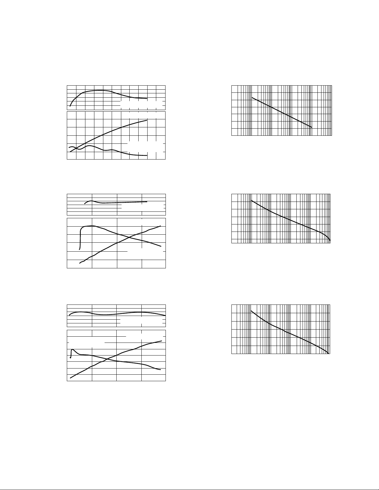
Typical Performance @ 25ºC Case Temperature (continued)
17
16
15
14
13
POWER
12
11
OUTPUT, dBm
1670
1435
1206
MHz
974
742
FREQUENCY,
0
0
2468 22
TUNING VOLTAGE, VDC
POWER OUTPUT
TUNING CURVE
MODULATION
SENSITIVITY
10 12 14 16 18 20
Figure 7. VTO-9090 Power Output, Frequency
and Modulation Sensitivity vs. Tuning Voltage.
16
14
12
POWER
10
2500
OUTPUT, dBm
2000
MHz
1500
FREQUENCY,
1000
0
520
TUNING VOLTAGE, VDC
POWER OUTPUT
TUNING CURVE
MODULATION
SENSITIVITY
10 15
Figure 9. VTO-9120 Power Output, Frequency
and Modulation Sensitivity vs. Tuning Voltage.
–20
–40
–60
–80
250
200
150
100
MODULATION
50
0
100
0
SENSITIVITY, MHz/V
MODULATION
SENSITIVITY, MHz/V
–100
–120
LOG £(f), dBc/Hz
–140
–160
Figure 8. VTO-9090 Noise @ 1000 MHz
Single Sideband Phase Noise.
–40
–60
–80
–100
–120
–140
LOG £(f), dBc/Hz
–160
Figure 10. VTO-9120 Normalized Phase Noise
@ 2000 MHz S.S.B. Power Spectral Density.
1K 10K 100K 1M 10M
FOURIER FREQUENCY, Hz
1K 10K 100K 1M 10M
FOURIER FREQUENCY, Hz
16
14
12
10
POWER
3000
OUTPUT, dBm
2500
2000
MHz
1500
FREQUENCY,
1000
05 2010 15
MODULATION
SENSITIVITY
TUNING VOLTAGE, VDC
POWER OUTPUT
TUNING CURVE
Figure 11. VTO-9130 Power Output, Frequency
and Modulation Sensitivity vs. Tuning Voltage.
200
100
MODULATION
0
–40
–60
–80
–100
–120
LOG £(f), dBc/Hz
–140
–160
SENSITIVITY, MHz/V
9-33
1K 10K 100K 1M 10M
FOURIER FREQUENCY, Hz
Figure 12. VTO-9130 Normalized Phase Noise
@ 2300 MHz S.S.B. Power Spectral Density.
Page 5
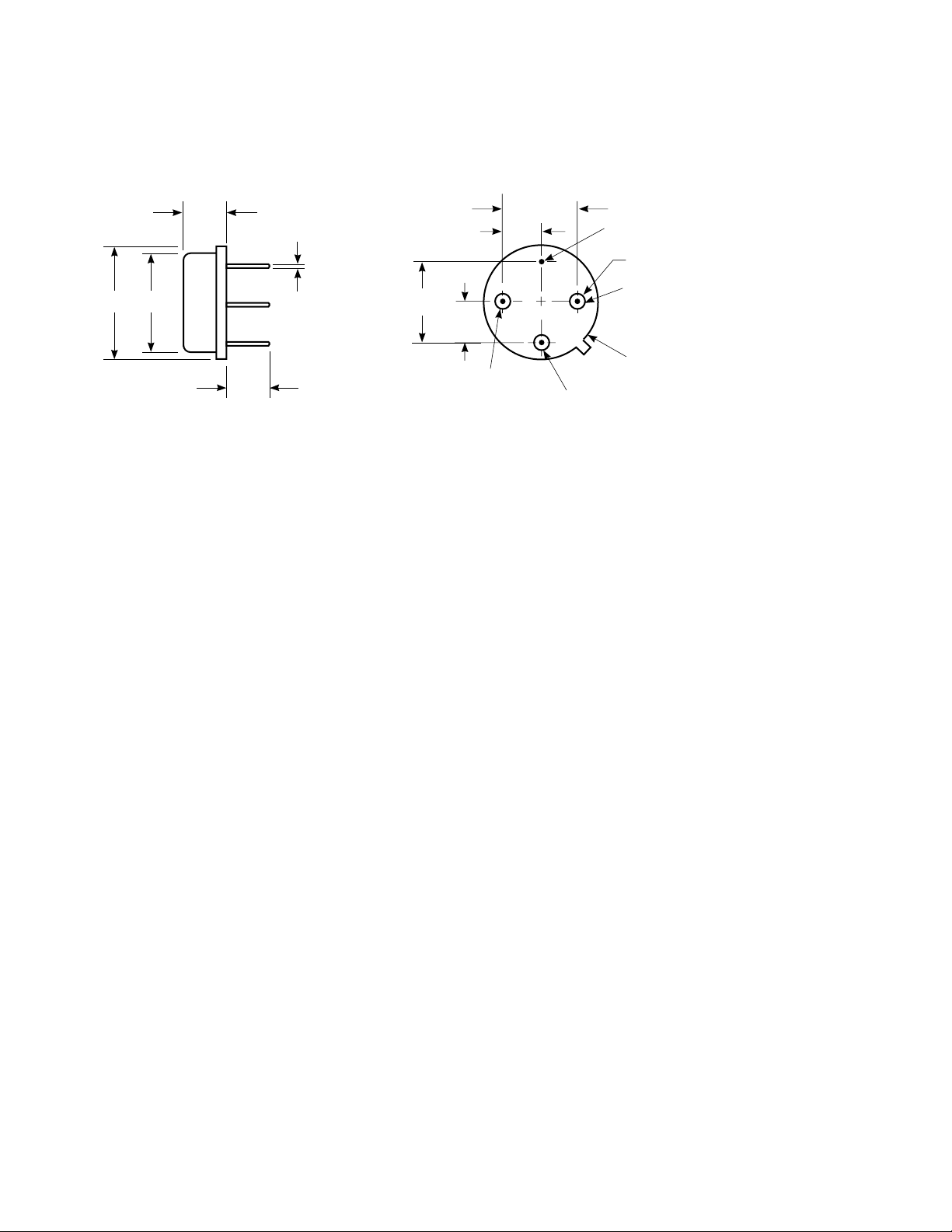
TO-8V Case Drawing
.20
.50
.45
DIA
DIA
0.22
MIN
.017 +.002
–.001
.300
TYP
.150
TYP
.150
TYP
.300
TYP
3
2
1
V
TUNE
APPROXIMATE WEIGHT 1.7 GRAMS
NOTES (UNLESS OTHERWISE SPECIFIED):
1. DIMENSIONS ARE SPECIFIED IN INCHES
2. TOLERANCES: xx ± .02
GROUND
GLASS RING
.060 DIA TYP
4
GROUND
+
V
xxx ± .010
RF OUT
(3X)
CASE
Test Fixtures for
TO-8␣ Packages
(TF 801/802)
Oscillators (VTO)
Features
• DC to 11 GHz Frequency
Range
• Connectorized Tuning Port
and RF Output
• Easy to Test Package
• Repeatable Performance
Applications
• Engineering
Characterization
• Incoming Inspection
• System Prototype
• Demonstration of Device
Performance
Description
To facilitate testing and
prototyping of products in the
TO-8V package, a series of test
fixtures is available. Designated
the HP TF Series test fixtures,
they feature rugged construction
for precise, repeatable
measurements.
The TF Series test fixtures come
supplied with mounting hardware
to ensure excellent ground
contact between the oscillator
package and test fixture. This
assures excellent contact between
package pins and test fixture
connector pins for reliable testing.
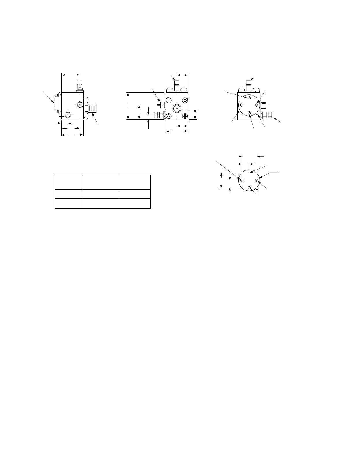
The device under test is aligned
according to Figure 13, and
pushed fully down onto the
fixture. The steel mounting ring
clamp is placed over the device
under test and secured by machine screws prior to testing.
Orientation of pins can be verified
by comparison with part (c) of
Figure 13. It is recommended that
both machine screws be used to
fasten the ring clamp. Screws
should be tightened down snugly
with a jewelers type screwdriver.
For different connector options
check the table in Figure 13 to
identify the correct part numbers.
It should be noted that some
output power variation may be
seen, from unit data, at frequencies above 8 GHz. This is
due to small differences in lengths
of test fixture RF output
connector pins.
9-34
Page 6
VTO IN
PLACE
.53
TUNING VOLTAGE
CONNECTOR
POWER INPUT
CONNECTOR
.35
+ TUNING
VOLTAGE
PIN
TUNING VOLTAGE
DC
PIN
GROUND
.20
.55
RF
OUT
.65
CONNECTOR OPTIONS
SERIES
TF-801
TF-802
TUNING
VOLTAGE
SMA
SMA
Figure 13. TO-8 Test Fixture.
.83
.45
RF
OUTPUT
SMA
TYPE N
.15
.70
(b)(a)
.35
.35
+ TUNING
VOLTAGE
GROUND
.150
TYP
.45
.150
TYP
RF
OUT
(c)
.300
TYP
3
4
2
1
+DC VOLTAGE
(Bottom View)
V
DC
GROUND
TAB ON PACKAGE
GROUND
CASE
GROUND
RF
OUT
9-35
 Loading...