

Page 1
Features
VNS3NV04D-E
OMNIFET II
fully autoprotected Power MOSFET
Max On-State resistance (per ch.) R
Current limitation (typ) I
Drain-Source clamp voltage V
■ Linear current limitation
■ Thermal shut down
■ Short circuit protection
■ Integrated clamp
■ Low current drawn from input pin
■ Diagnostic feedback through input pin
■ Esd protection
■ Direct access to the gate of the power mosfet
LIMH
CLAMP
ON
120mΩ
3.5A
40V
(analog driving)
■ Compatible with standard power mosfet
SO-8
Description
The VNS3NV04D-E is a device formed by two
monolithic OMNIFET II chips housed in a
standard SO-8 package. The OMNIFET II are
designed in STMicroelectronics VIPower M0-3
Technology: they are intended for replacement of
standard Power MOSFETs from DC up to 50KHz
applications. Built in thermal shutdown, linear
current limitation and overvoltage clamp protects
the chip in harsh environments.
Fault feedback can be detected by monitoring the
voltage at the input pin.
Table 1. Device summary
Package
SO-8 VNS3NV04D-E VNS3NV04DTR-E
July 2007 Rev 2 1/21
Order codes
Tube Tape and Reel
www.st.com
21
Page 2

Contents VNS3NV04D-E
Contents
1 Block diagram and pin description . . . . . . . . . . . . . . . . . . . . . . . . . . . . . 5
2 Electrical specifications . . . . . . . . . . . . . . . . . . . . . . . . . . . . . . . . . . . . . . 6
2.1 Absolute maximum ratings . . . . . . . . . . . . . . . . . . . . . . . . . . . . . . . . . . . . . 6
2.2 Thermal data . . . . . . . . . . . . . . . . . . . . . . . . . . . . . . . . . . . . . . . . . . . . . . . 7
2.3 Electrical characteristics . . . . . . . . . . . . . . . . . . . . . . . . . . . . . . . . . . . . . . . 7
2.4 Electrical characteristics curves . . . . . . . . . . . . . . . . . . . . . . . . . . . . . . . . 12
3 Protection features . . . . . . . . . . . . . . . . . . . . . . . . . . . . . . . . . . . . . . . . . 16
3.1 Overvoltage clamp protection . . . . . . . . . . . . . . . . . . . . . . . . . . . . . . . . . . 16
3.2 Linear current limiter circuit . . . . . . . . . . . . . . . . . . . . . . . . . . . . . . . . . . . 16
3.3 Overtemperature and short circuit protection . . . . . . . . . . . . . . . . . . . . . . 16
3.4 Status feedback . . . . . . . . . . . . . . . . . . . . . . . . . . . . . . . . . . . . . . . . . . . . 16
4 Package and packing information . . . . . . . . . . . . . . . . . . . . . . . . . . . . . 17
4.1 ECOPACK® packages . . . . . . . . . . . . . . . . . . . . . . . . . . . . . . . . . . . . . . . 17
4.2 SO-8 Package mechanical data . . . . . . . . . . . . . . . . . . . . . . . . . . . . . . . . 18
4.3 SO-8 Packing information . . . . . . . . . . . . . . . . . . . . . . . . . . . . . . . . . . . . . 19
5 Revision history . . . . . . . . . . . . . . . . . . . . . . . . . . . . . . . . . . . . . . . . . . . 20
2/21
Page 3

VNS3NV04D-E List of tables
List of tables
Table 1. Device summary . . . . . . . . . . . . . . . . . . . . . . . . . . . . . . . . . . . . . . . . . . . . . . . . . . . . . . . . . . 1
Table 2. Absolute maximum ratings . . . . . . . . . . . . . . . . . . . . . . . . . . . . . . . . . . . . . . . . . . . . . . . . . . 6
Table 3. Thermal data. . . . . . . . . . . . . . . . . . . . . . . . . . . . . . . . . . . . . . . . . . . . . . . . . . . . . . . . . . . . . 7
Table 4. Off . . . . . . . . . . . . . . . . . . . . . . . . . . . . . . . . . . . . . . . . . . . . . . . . . . . . . . . . . . . . . . . . . . . . . 7
Table 5. On . . . . . . . . . . . . . . . . . . . . . . . . . . . . . . . . . . . . . . . . . . . . . . . . . . . . . . . . . . . . . . . . . . . . . 7
Table 6. Dynamic . . . . . . . . . . . . . . . . . . . . . . . . . . . . . . . . . . . . . . . . . . . . . . . . . . . . . . . . . . . . . . . . 8
Table 7. Switching . . . . . . . . . . . . . . . . . . . . . . . . . . . . . . . . . . . . . . . . . . . . . . . . . . . . . . . . . . . . . . . 8
Table 8. Source Drain diode . . . . . . . . . . . . . . . . . . . . . . . . . . . . . . . . . . . . . . . . . . . . . . . . . . . . . . . . 8
Table 9. Protections (-40°C < Tj < 150°C, unless otherwise specified) . . . . . . . . . . . . . . . . . . . . . . . 9
Table 10. Document revision history . . . . . . . . . . . . . . . . . . . . . . . . . . . . . . . . . . . . . . . . . . . . . . . . . 20
3/21
Page 4

List of figures VNS3NV04D-E
List of figures
Figure 1. Block diagram . . . . . . . . . . . . . . . . . . . . . . . . . . . . . . . . . . . . . . . . . . . . . . . . . . . . . . . . . . . . 5
Figure 2. Configuration diagram (top view) . . . . . . . . . . . . . . . . . . . . . . . . . . . . . . . . . . . . . . . . . . . . . 5
Figure 3. Current and voltage conventions . . . . . . . . . . . . . . . . . . . . . . . . . . . . . . . . . . . . . . . . . . . . . 6
Figure 4. Switching time test circuit for resistive load . . . . . . . . . . . . . . . . . . . . . . . . . . . . . . . . . . . . . 9
Figure 5. Test circuit for diode recovery times . . . . . . . . . . . . . . . . . . . . . . . . . . . . . . . . . . . . . . . . . . 10
Figure 6. Unclamped inductive load test circuits . . . . . . . . . . . . . . . . . . . . . . . . . . . . . . . . . . . . . . . . 10
Figure 7. Input charge test circuit. . . . . . . . . . . . . . . . . . . . . . . . . . . . . . . . . . . . . . . . . . . . . . . . . . . . 11
Figure 8. Unclamped inductive waveforms . . . . . . . . . . . . . . . . . . . . . . . . . . . . . . . . . . . . . . . . . . . . 11
Figure 9. Source-Drain diode forward characteristics . . . . . . . . . . . . . . . . . . . . . . . . . . . . . . . . . . . . 12
Figure 10. Static Drain-Source On resistance . . . . . . . . . . . . . . . . . . . . . . . . . . . . . . . . . . . . . . . . . . . 12
Figure 11. Derating curve . . . . . . . . . . . . . . . . . . . . . . . . . . . . . . . . . . . . . . . . . . . . . . . . . . . . . . . . . . 12
Figure 12. Static Drain-Source On resistance vs. Input voltage . . . . . . . . . . . . . . . . . . . . . . . . . . . . . 12
Figure 13. Static Drain-Source On resistance Vs. Input voltage . . . . . . . . . . . . . . . . . . . . . . . . . . . . . 12
Figure 14. Transconductance . . . . . . . . . . . . . . . . . . . . . . . . . . . . . . . . . . . . . . . . . . . . . . . . . . . . . . . 12
Figure 15. Static Drain-Source On resistance Vs. Id . . . . . . . . . . . . . . . . . . . . . . . . . . . . . . . . . . . . . . 13
Figure 16. Transfer characteristics . . . . . . . . . . . . . . . . . . . . . . . . . . . . . . . . . . . . . . . . . . . . . . . . . . . 13
Figure 17. Turn On current slope . . . . . . . . . . . . . . . . . . . . . . . . . . . . . . . . . . . . . . . . . . . . . . . . . . . . . 13
Figure 18. Turn On current slope . . . . . . . . . . . . . . . . . . . . . . . . . . . . . . . . . . . . . . . . . . . . . . . . . . . . . 13
Figure 19. Input voltage Vs. Input charge . . . . . . . . . . . . . . . . . . . . . . . . . . . . . . . . . . . . . . . . . . . . . . 13
Figure 20. Turn off Drain source voltage slope . . . . . . . . . . . . . . . . . . . . . . . . . . . . . . . . . . . . . . . . . . 13
Figure 21. Turn off Drain-Source voltage slope . . . . . . . . . . . . . . . . . . . . . . . . . . . . . . . . . . . . . . . . . . 14
Figure 22. Capacitance variations . . . . . . . . . . . . . . . . . . . . . . . . . . . . . . . . . . . . . . . . . . . . . . . . . . . . 14
Figure 23. Switching time resistive load. . . . . . . . . . . . . . . . . . . . . . . . . . . . . . . . . . . . . . . . . . . . . . . . 14
Figure 24. Switching time resistive load. . . . . . . . . . . . . . . . . . . . . . . . . . . . . . . . . . . . . . . . . . . . . . . . 14
Figure 25. Output characteristics . . . . . . . . . . . . . . . . . . . . . . . . . . . . . . . . . . . . . . . . . . . . . . . . . . . . . 14
Figure 26. Normalized On resistance Vs. temperature . . . . . . . . . . . . . . . . . . . . . . . . . . . . . . . . . . . . 14
Figure 27. Normalized Input threshold voltage Vs. temperature . . . . . . . . . . . . . . . . . . . . . . . . . . . . . 15
Figure 28. Normalized current limit Vs. junction temperature . . . . . . . . . . . . . . . . . . . . . . . . . . . . . . . 15
Figure 29. Step response current limit . . . . . . . . . . . . . . . . . . . . . . . . . . . . . . . . . . . . . . . . . . . . . . . . . 15
Figure 30. SO-8 package mechanical data & package outline . . . . . . . . . . . . . . . . . . . . . . . . . . . . . . 18
Figure 31. SO-8 tube shipment (no suffix) . . . . . . . . . . . . . . . . . . . . . . . . . . . . . . . . . . . . . . . . . . . . . . 19
Figure 32. SO-8 tape and reel shipment (suffix “TR”) . . . . . . . . . . . . . . . . . . . . . . . . . . . . . . . . . . . . . 19
4/21
Page 5
VNS3NV04D-E Block diagram and pin description
1 Block diagram and pin description
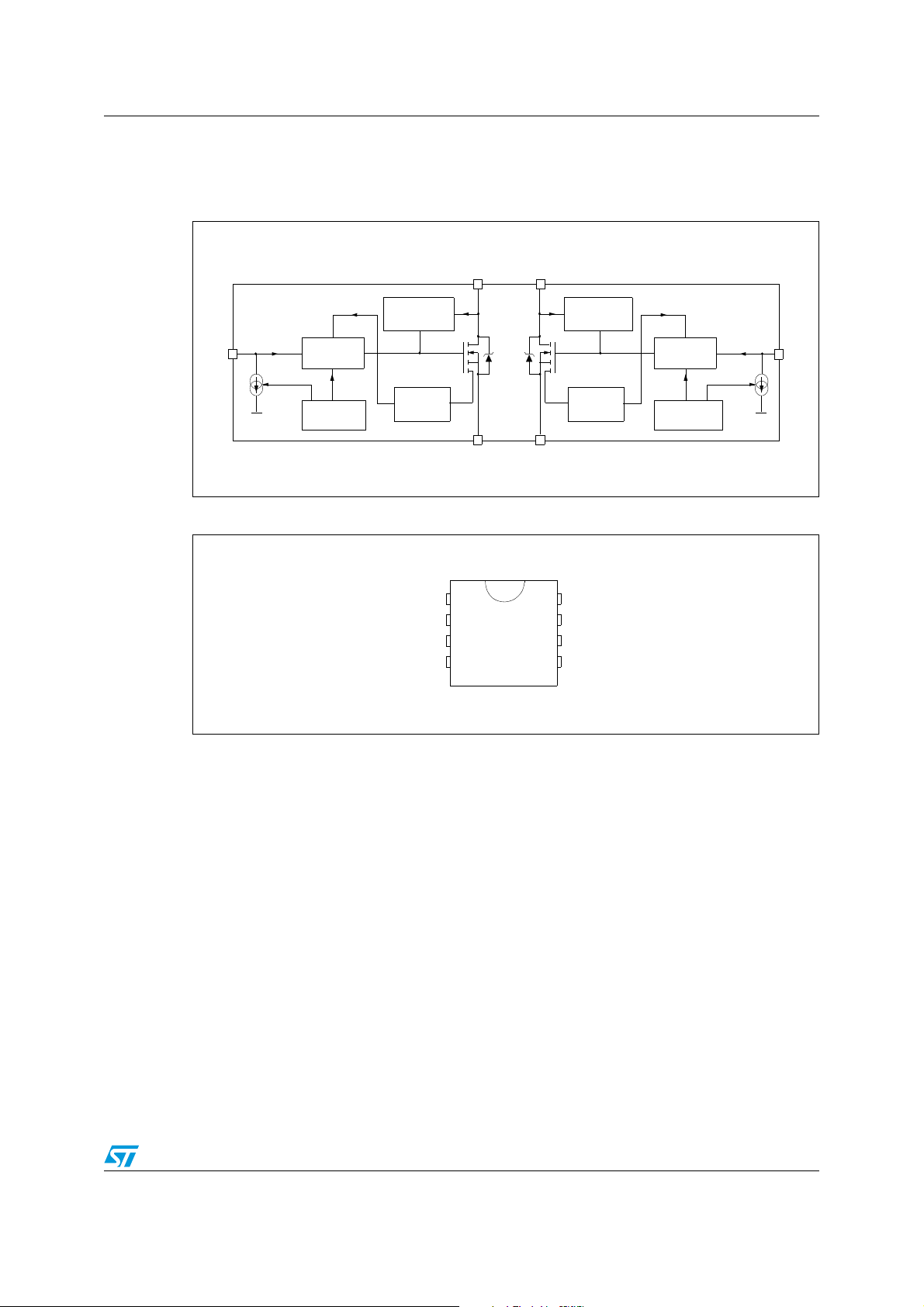
Figure 1. Block diagram
DRAIN1
OVERVO LTAGE
CLAMP
INPUT1
GATE
CONTROL
OVER
TEMPERATURE
LINEAR
CURRENT
LIMITER
SOURCE1
Figure 2. Configuration diagram (top view)
SOURCE 1
INPUT 1
SOURCE 2
INPUT 2
1
4
DRAIN2
SOURCE2
8
5
OVERVO LTAGE
CLAMP
LINEAR
CURRENT
LIMITER
DRAIN 1
DRAIN 1
DRAIN 2
DRAIN 2
GATE
CONTROL
OVER
TEMPERATURE
INPUT2
5/21
Page 6
Electrical specifications VNS3NV04D-E
2 Electrical specifications
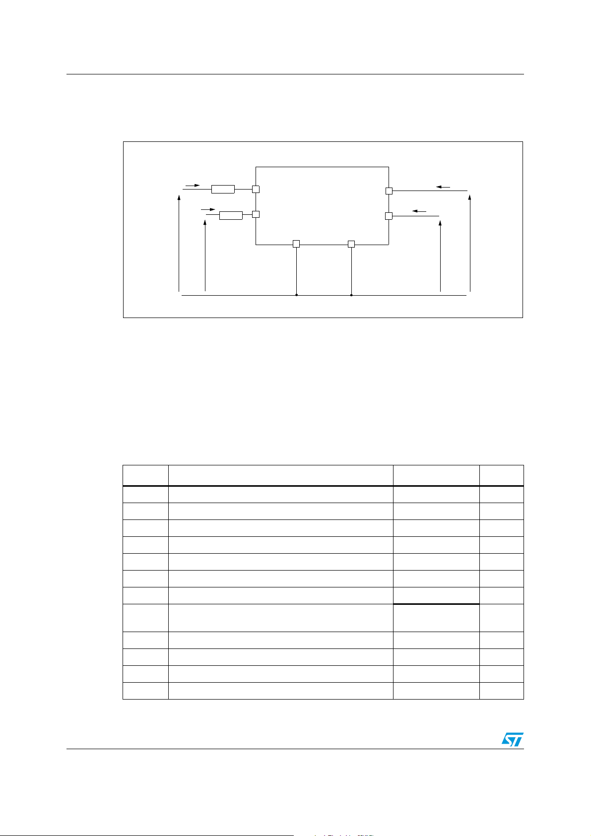
Figure 3. Current and voltage conventions
IN2
R
IN1
INPUT 1
I
R
IN2
IN2
INPUT 2
SOURCE 1
I
IN1
V
IN1
V
2.1 Absolute maximum ratings
Stressing the device above the rating listed in the “Absolute maximum ratings” table may
cause permanent damage to the device. These are stress ratings only and operation of the
device at these or any other conditions above those indicated in the operating sections of
this specification is not implied. Exposure to Absolute maximum rating conditions for
extended periods may affect device reliability. Refer also to the STMicroelectronics SURE
program and other relevant quality document.
Table 2. Absolute maximum ratings
DRAIN 1
DRAIN 2
SOURCE 2
I
D1
I
D2
V
DS1
V
DS1
Symbol Parameter Value Unit
V
V
I
R
IN MINn
I
I
V
ESD1
V
ESD2
P
T
Drain-Source Voltage (V
DSn
Input voltage Internally clamped V
INn
Input current +/-20 mA
INn
=0V) Internally clamped V
INn
Minimum input series impedance 220 Ω
Drain current Internally limited A
Dn
Reverse DC output current -5.5 A
Rn
Electrostatic discharge (R=1.5KΩ, C=100pF) 4000 V
Electrostatic discharge on output pins only (R=330Ω,
C=150pF)
Total dissipation at Tc=25°C 4 Ω
tot
Operating junction temperature Internally limited °C
T
j
Case operating temperature Internally limited °C
T
c
Storage temperature -55 to 150 °C
stg
6/21
16500 V
Page 7
VNS3NV04D-E Electrical specifications
2.2 Thermal data
Table 3. Thermal data
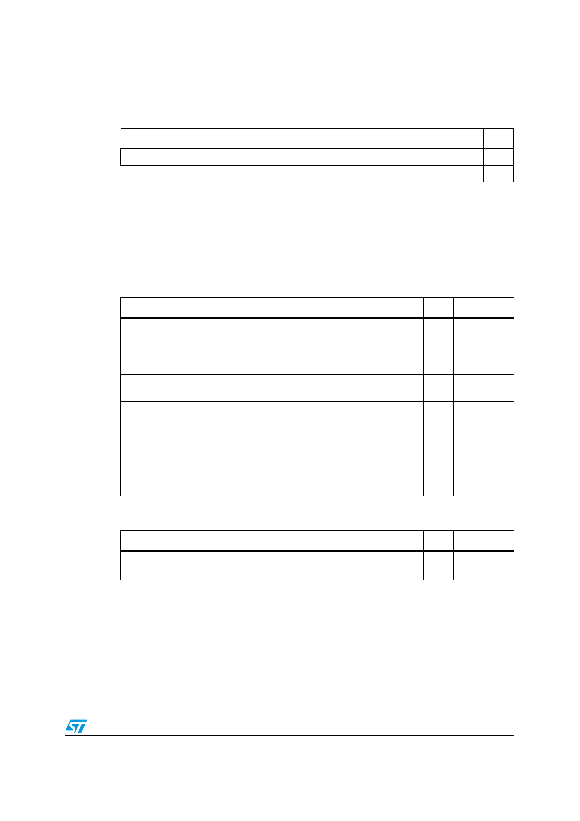
Symbol Parameter Max value Unit
R
thj-lead
R
thj-amb
1. When mounted on a standard single-sided FR4 board with 50mm2 of Cu (at least 35 µm thick) connected
to all DRAIN pins of the relative channel
Thermal resistance junction-lead (per channel) 30 °C/W
Thermal resistance junction-ambient 80
2.3 Electrical characteristics
Values specified in this section are for -40°C< Tj <150°C, unless otherwise stated.
Table 4. Off
Symbol Parameter Test Conditions Min Typ Max Unit
V
CLAMP
V
CLTH
V
INTH
I
V
INCL
Drain-Source clamp
voltage
Drain-Source clamp
threshold voltage
Input threshold
voltage
Supply current from
ISS
input pin
Input-Source clamp
voltage
VIN=0V; ID=1.5A 40 45 55 V
=0V; ID=2mA 36 V
V
IN
V
DS=VIN
V
=0V; VIN=5V 100 150 µA
DS
IIN=1mA
IIN=-1mA
(1)
°C/W
; ID=1mA 0.5 2.5 V
6
6.8 8
-1.0
-0.3
V
I
DSS
Zero input voltage
drain current
(VIN=0V)
VDS=13V; VIN=0V; Tj=25°C
VDS=25V; VIN=0V
30
75
Table 5. On
Symbol Parameter Test conditions Min Typ Max Unit
R
DS(on)
Static Drain-Source
On resistance
=5V; ID=1.5A; Tj=25°C
V
IN
=5V; ID=1.5A
V
IN
7/21
120
240
µA
mΩ
Page 8
Electrical specifications VNS3NV04D-E
Electrical characteristics (continued) (Tj=25°C, unless otherwise specified)
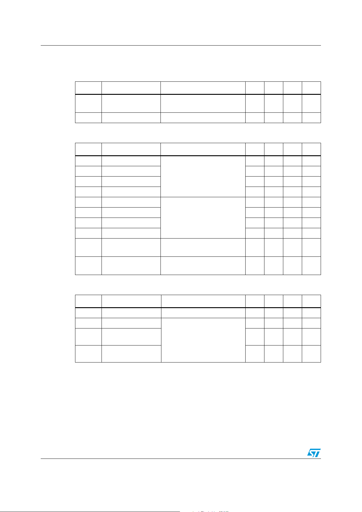
Table 6. Dynamic
Symbol Parameter Test conditions Min Typ Max Unit
Forward
(1)
g
C
fs
OSS
transconductance
Output capacitance VDS=13V; f=1MHz; VIN=0V 150 pF
VDD=13V; ID=1.5A 5.0 S
Table 7. Switching
Symbol Parameter Test conditions Min Typ Max Unit
t
d(on)
t
d(off)
t
d(on)
t
d(off)
(dI/dt)
Turn-on delay time
V
=15V; ID=1.5A
t
Rise Time 250 750 ns
r
Turn-off delay time 450 1350 ns
t
Fall time 250 750 ns
f
DD
V
=5V; R
gen
gen=RIN MIN
(see Figure 4)
=220Ω
Turn-on delay time
=15V; ID=1.5A
V
Rise time 2.5 7.5 µs
t
r
Turn-off delay time 3.3 10.0 µs
Fall time 2.0 6.0 µs
t
f
Turn-on current slope
on
Q
Total input charge
i
DD
V
gen
=5V; R
=2.2 KΩ
gen
(see Figure 4)
V
=15V; ID=1.5A
DD
=5V; R
V
gen
V
DD
=2.13mA (see Figure 7)
I
gen
gen=RIN MIN
=12V; ID=1.5A; VIN=5V
=220Ω
90 300 ns
0.45 1.35 µs
4.7 A/µs
8.5 nC
Table 8. Source Drain diode
Symbol Parameter Test Conditions Min Typ Max Unit
(1)
V
SD
Q
I
RRM
1. Pulsed: Pulse duration = 300µs, duty cycle 1.5%
Forward On voltage ISD=1.5A; VIN=0V 0.8 V
t
Reverse recovery time
rr
Reverse recovery
rr
charge
Reverse recovery
current
=1.5A; dI/dt=12A/µs
I
SD
=30V; L=200µH
V
DD
(see Figure 5)
107 ns
37 µC
0.7 A
8/21
Page 9
VNS3NV04D-E Electrical specifications
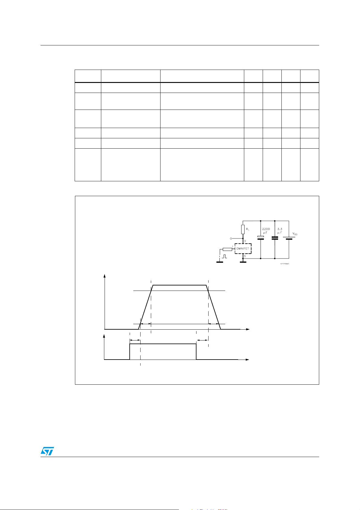
Table 9. Protections (-40°C < Tj < 150°C, unless otherwise specified)
Symbol Parameter Test Conditions Min Typ Max Unit
I
t
dlim
T
T
Eas
Drain current limit VIN=5V; VDS=13V 3.5 5 7 A
lim
Step response current
limit
Overtemperature
jsh
shutdown
Overtemperature reset 135 °C
jrs
I
Fault sink current VIN=5V; VDS=13V; Tj=T
gf
Single pulse
avalanche energy
VIN=5V; VDS=13V 10 µs
150 175 200 °C
10 15 20 mA
100 mJ
Starting T
=5V R
V
IN
L=24mH
jsh
=25°C; VDD=24V
j
gen=RIN MIN
=220Ω;
(see Figure 6 and Figure 8)
Figure 4.
Switching time test circuit for resistive load
V
R
gen
V
gen
D
I
D
90%
t
d(off)
t
f
t
t
t
r
t
V
gen
d(on)
10%
9/21
Page 10
Electrical specifications VNS3NV04D-E
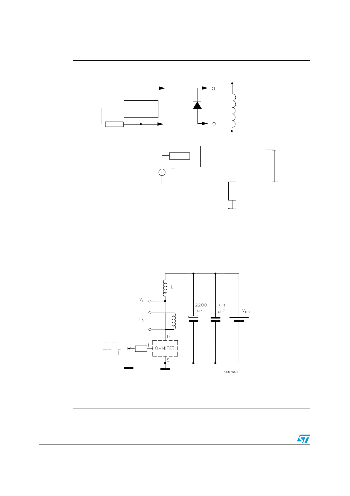
Figure 5.
Test circuit for diode recovery times
A
D
220
I
OMNIFET
Ω
S
V
gen
FAS T
DIODE
B
R
gen
I
A
B
OMNIFET
L=100uH
D
S
8.5
V
DD
Ω
Figure 6. Unclamped inductive load test circuits
R
V
IN
P
W
GEN
10/21
Page 11
VNS3NV04D-E Electrical specifications
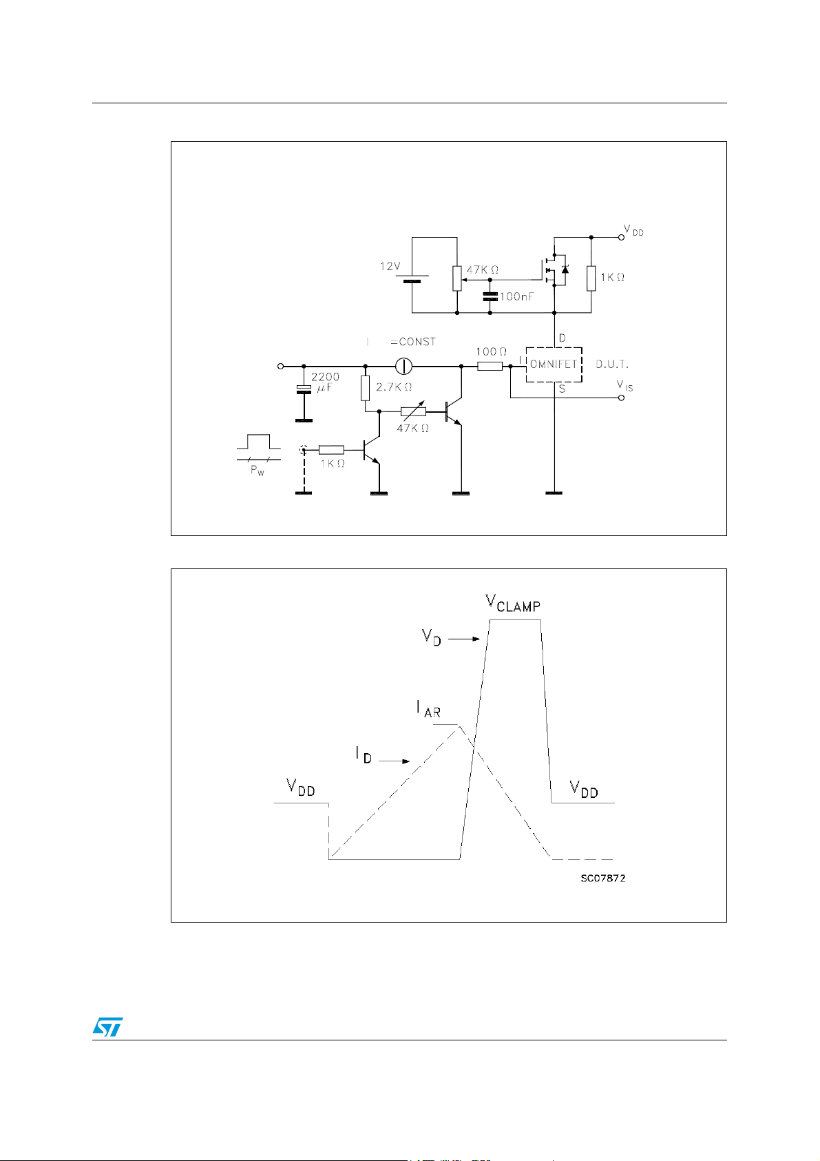
Figure 7. Input charge test circuit
IN
V
GEN
Figure 8. Unclamped inductive waveforms
ND8003
11/21
Page 12
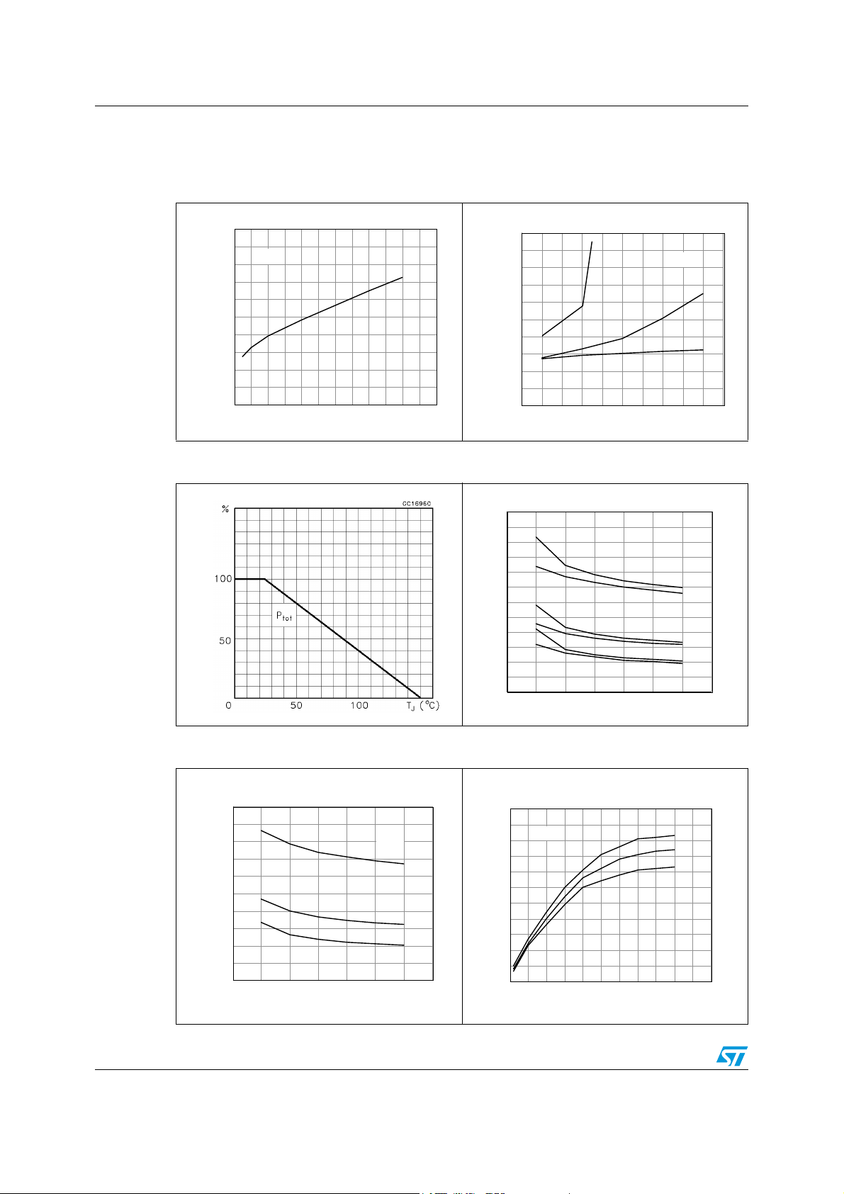
Electrical specifications VNS3NV04D-E
2.4 Electrical characteristics curves
Figure 9. Source-Drain diode forward
characteristics
Vsd (mV)
1100
1050
1000
Vin=0V
950
900
850
800
750
700
650
600
0123456789101112
Id (A )
Figure 10. Static Drain-Source On
resistance
Rds(on) (mohms)
1000
900
800
700
600
500
400
300
200
100
0
0.05 0.1 0.15 0.2 0.25 0.3 0.35 0.4 0.45 0.5 0.55
Tj=-40ºC
Vin=2.5V
Tj=25ºC
Tj=150ºC
Id(A )
Figure 11. Derating curve Figure 12. Static Drain-Source On
resistance vs. Input voltage
Rds (on) (mohms)
300
275
250
Tj=150ºC
225
200
175
150
Tj=25ºC
125
100
Tj=-40ºC
75
50
25
0
3 3.5 4 4.5 5 5.5 6 6.5
Id=3.5A
Id=1A
Id =3.5A
Id =1A
Id=3.5A
Id=1A
Vin(V)
Figure 13. Static Drain-Source On
Figure 14. Transconductance
resistance Vs. Input voltage
Rds (on) (mohms)
250
225
200
175
150
125
100
75
50
25
0
3 3.5 4 4.5 5 5.5 6 6.5
Vin(V)
Id =1.5 A
Tj=150ºC
Tj=25ºC
Tj=-40ºC
12/21
Gfs (S)
11
10
Vds=13V
9
8
7
6
5
4
3
2
1
0
0 0.5 1 1.5 2 2.5 3 3.5 4 4 .5 5 5.5
Id ( A )
Tj=-40ºC
Tj=25ºC
Tj=150ºC
Page 13
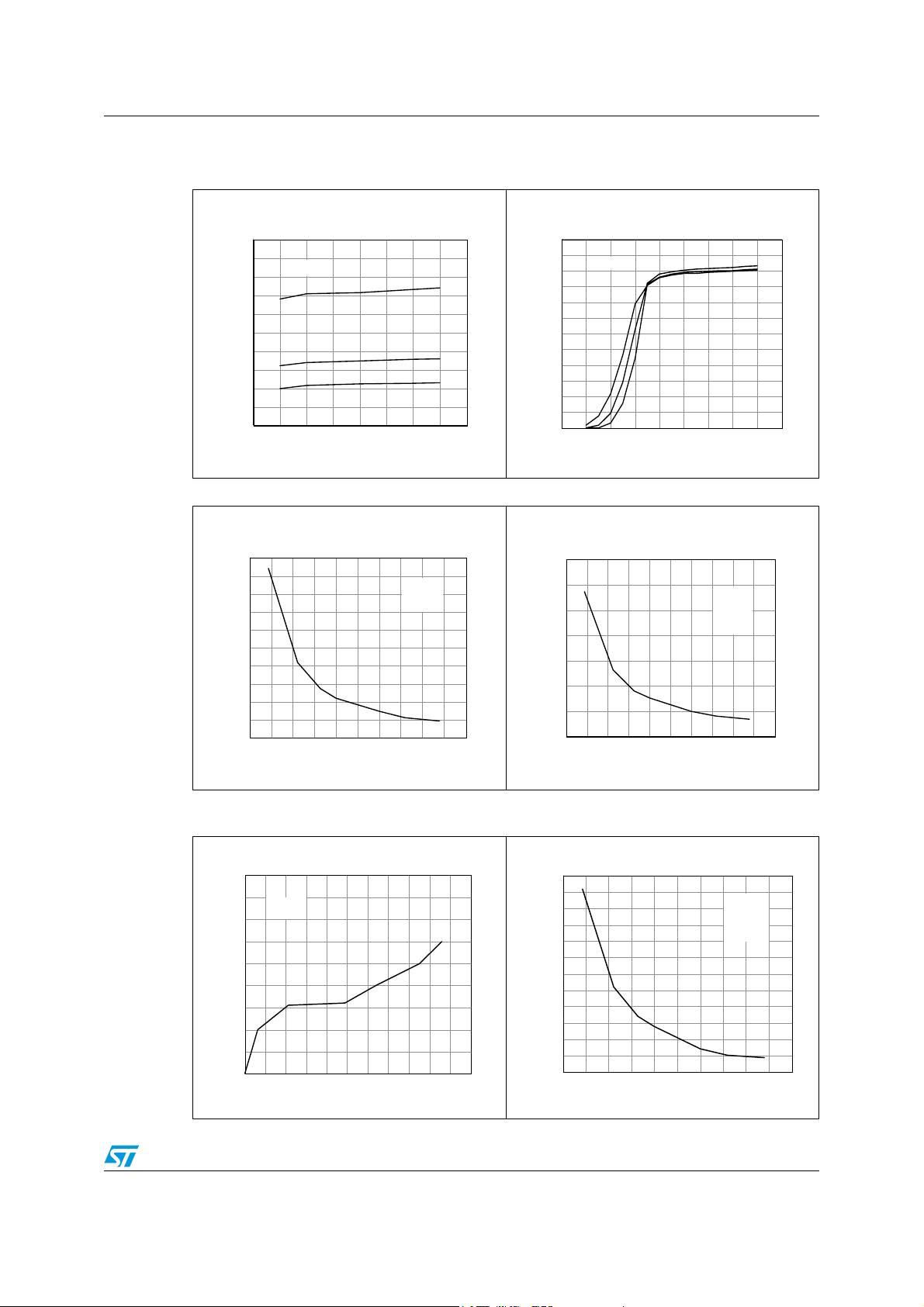
VNS3NV04D-E Electrical specifications
Figure 15. Static Drain-Source On
Figure 16. Transfer characteristics
resistance Vs. Id
R ds (on) (mo hms)
250
225
200
175
150
125
100
75
50
25
0
Vin=5V
Tj=150ºC
Tj=25ºC
Tj= - 40ºC
0 0.5 1 1.5 2 2 .5 3 3.5 4
Id (A )
Ido n (A )
6
5.5
Vds=13 .5V
5
4.5
4
3.5
3
2.5
2
1.5
0.5
0
Tj=150ºC
Tj=-40ºC
Tj=25ºC
1
1.5 2 2.5 3 3.5 4 4.5 5 5.5 6
Vin (V)
Figure 17. Turn On current slope Figure 18. Turn On current slope
di/dt(A/us)
5
4.5
4
3.5
3
2.5
2
1.5
1
0.5
0
0
Vin=5V
Vdd=15V
Id =1.5A
500
1000
1500
2000
250
750
1250
1750
2250
2500
Rg(ohm)
di/dt(A/usec)
1.75
1.5
1.25
1
0.75
0.5
0.25
0
0
Vin=3. 5V
Vdd=15V
Id =1. 5A
250
750
1250
500
1000
Rg(ohm)
1500
1750
2000
2250
2500
Figure 19. Input voltage Vs. Input
charge
Vin (V)
9
8
Vds=1V
Id =1. 5A
7
6
5
4
3
2
1
0
012345 67891011
Qg (nC)
Figure 20. Turn off Drain source voltage
slope
dv/dt(V/usec)
300
275
250
225
200
175
150
125
100
75
50
25
0
0
500
750
1000
1250
250
Rg(ohm)
13/21
1500
Vdd=15V
1750
Vin=5V
Id =1.5A
2000
2250
2500
Page 14
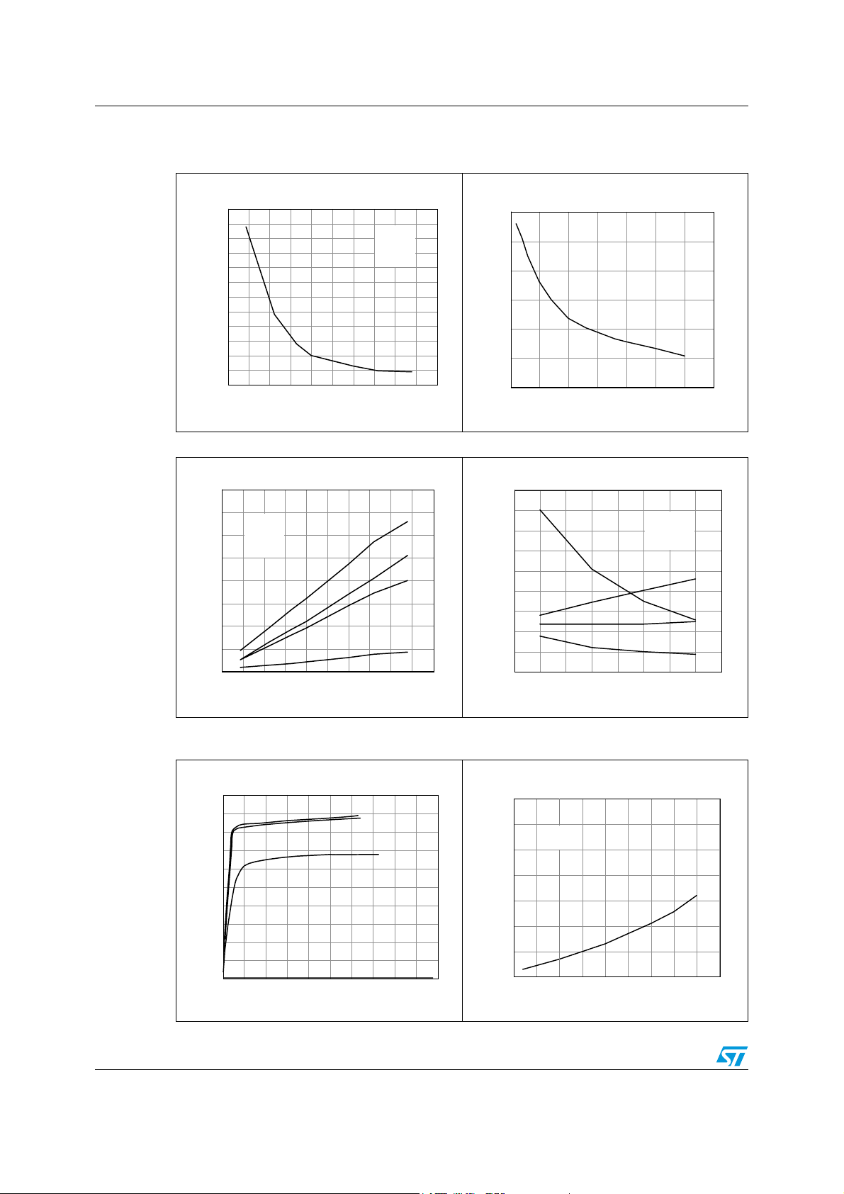
Electrical specifications VNS3NV04D-E
Figure 21. Turn off Drain-Source voltage
Figure 22. Capacitance variations
slope
dv/dt(V/usec)
300
275
250
225
200
175
150
125
100
75
50
25
0
0
250
500
750
1000
1250
Rg(ohm)
1500
1750
Vin=3.5V
Vdd=15V
Id =1.5A
2000
2250
2500
C(pF)
350
300
250
200
150
100
50
0 5 10 15 20 25 30 35
Vds(V)
f=1MHz
Vin=0V
Figure 23. Switching time resistive load Figure 24. Switching time resistive load
t(us ec )
4
3.5
3
2.5
2
1.5
1
0.5
0
Vdd=15V
Id =1.5A
Vin=5V
td(off)
tr
tf
td(on)
0
500
1000
1500
250
750
1250
1750
2000
2250
2500
Rg(ohm)
t(ns ec)
900
800
700
600
500
400
300
200
100
0
3.25 3.5 3.75 4 4.25 4.5 4.75 5 5.25
td(off)
tf
td(on )
tr
Vdd=15V
Id =1.5A
Rg=220oh m
Vin(V)
Figure 25. Output characteristics Figure 26. Normalized On resistance Vs.
Id ( A )
5
4.5
4
3.5
3
2.5
2
1.5
1
0.5
0
012345678910
Vds (V)
14/21
Vin=5V
Vin=4V
Vin=3V
temperature
Rds(on) (mOhm)
4
3.5
3
2.5
2
1.5
0.5
Vin=5V
Id =1.5A
1
-50 -25 0 25 50 75 100 125 150 175
Tc )ºC )
Page 15
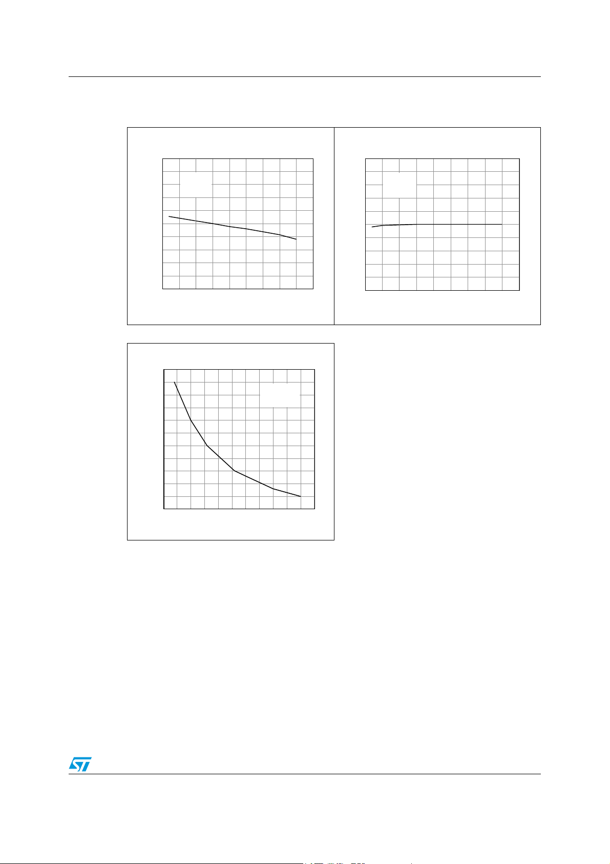
VNS3NV04D-E Electrical specifications
Figure 27. Normalized Input threshold
voltage Vs. temperature
Figure 28. Normalized current limit Vs.
junction temperature
Vinth (V)
2
1.8
1.6
1.4
1.2
0.8
0.6
0.4
0.2
0
Vds=Vin
Id =1mA
1
-50 -25 0 25 50 75 100 125 150 175
Tc (ºC )
Figure 29. Step response current limit
Tdlim(usec)
13
12.5
12
11.5
11
10.5
10
9.5
9
8.5
8
7.5
5 7.5 10 12.5 15 17.5 20 22.5 25 27.5 30 32.5
Vdd(V)
Vin=5V
Rg=220oh m
Ili m (A )
10
9
8
7
6
5
4
3
2
1
0
Vin=5V
Vds=13V
-50 -25 0 25 50 75 100 125 150 175
Tc ( ºC )
15/21
Page 16

Protection features VNS3NV04D-E
3 Protection features
During normal operation, the INPUT pin is electrically connected to the gate of the internal
power MOSFET through a low impedance path.
The device then behaves like a standard power MOSFET and can be used as a switch from
DC up to 50KHz. The only difference from the user’s standpoint is that a small DC current
I
(typ. 100µA) flows into the INPUT pin in order to supply the internal circuitry.
ISS
The device integrates:
3.1 Overvoltage clamp protection
Internally set at 45V, along with the rugged avalanche characteristics of the Power MOSFET
stage give this device unrivalled ruggedness and energy handling capability. This feature is
mainly important when driving inductive loads.
3.2 Linear current limiter circuit
Limits the drain current ID to I
is active, the device operates in the linear region, so power dissipation may exceed the
capability of the heatsink. Both case and junction temperatures increase, and if this phase
lasts long enough, junction temperature may reach the overtemperature threshold T
whatever the INPUT pin voltages. When the current limiter
lim
3.3 Overtemperature and short circuit protection
These are based on sensing the chip temperature and are not dependent on the input
voltage. The location of the sensing element on the chip in the power stage area ensures
fast, accurate detection of the junction temperature. Overtemperature cutout occurs in the
range 150 to 190 °C, a typical value being 170 °C. The device is automatically restarted
when the chip temperature falls of about 15°C below shut-down temperature.
3.4 Status feedback
In the case of an overtemperature fault condition (Tj > T
diagnostic current I
a low impedance source, this current may be used in order to warn the control circuit of a
device shutdown. If the drive impedance is high enough so that the INPUT pin driver is not
able to supply the current I
device operation: no requirement is put on the current capability of the INPUT pin
driver except to be able to supply the normal operation drive current I
Additional features of this device are ESD protection according to the Human Body model
and the ability to be driven from a TTL Logic circuit.
through the INPUT pin in order to indicate fault condition. If driven from
gf
, the INPUT pin will fall to 0V. This will not however affect the
gf
), the device tries to sink a
jsh
ISS
jsh.
.
16/21
Page 17

VNS3NV04D-E Package and packing information
4 Package and packing information
4.1 ECOPACK® packages
In order to meet environmental requirements, ST offers these devices in ECOPACK®
packages. These packages have a Lead-free second-level interconnect. The category of
Second-Level Interconnect is marked on the package and on the inner box label, in
compliance with JEDEC Standard JESD97. The maximum ratings related to soldering
conditions are also marked on the inner box label.
ECOPACK is an ST trademark. ECOPACK specifications are available at: www.st.com.
17/21
Page 18
Package and packing information VNS3NV04D-E
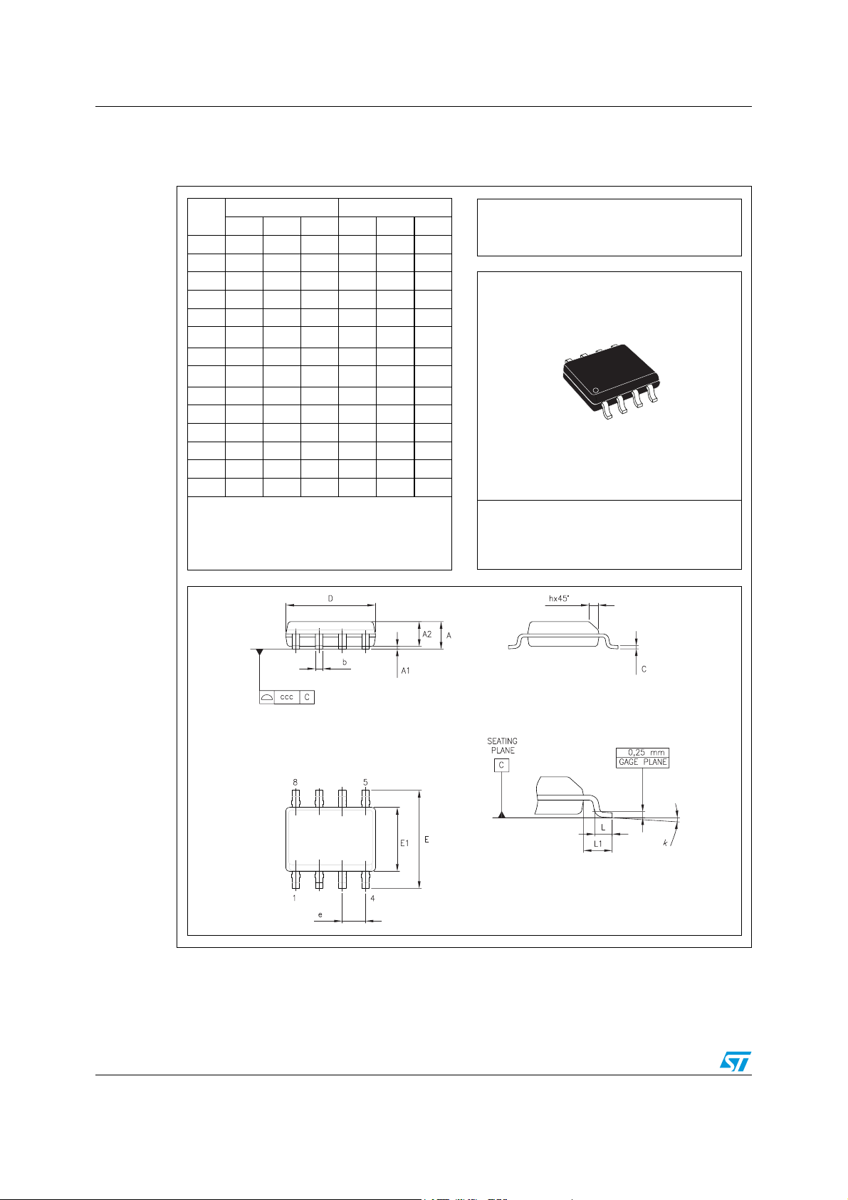
4.2 SO-8 Package mechanical data
Figure 30. SO-8 package mechanical data & package outline
DIM.
A 1.750 0.0689
A1 0.100 0.250 0.0039 0.0098
A2 1.250 0.0492
b 0.280 0.480 0.0110 0.0189
c 0.170 0.230 0.0067 0.0091
(1)
D
E 5.800 6.000 6.200 0.2283 0.2362 0.2441
(2)
E1
e 1.270 0.0500
h 0.250 0.500 0.0098 0.0197
L 0.400 1.270 0.0157 0.0500
L1 1.040 0.0409
k0˚8˚0˚8˚
ccc 0.100 0.0039
Notes: 1. Dimensions D does not include mold flash,
protrusions or gate burrs.
Mold flash, po trusions or gate burrs shall not
exceed 0.15m m in total (bo th side).
2. Dimension “E1” does not include interlead flash
or protrusions. Interlead flash or protrusions shall
not exceed 0.25 mm per side.
mm inch
MIN. TYP. MAX. MIN. TYP. MAX.
4.800 4.900 5.000 0.1890 0.1929 0.1969
3.800 3.900 4.000 0.1496 0.1535 0.1575
OUTLINE AND
MECHANICAL DATA
SO-8
18/21
0016023 D
Page 19
VNS3NV04D-E Package and packing information
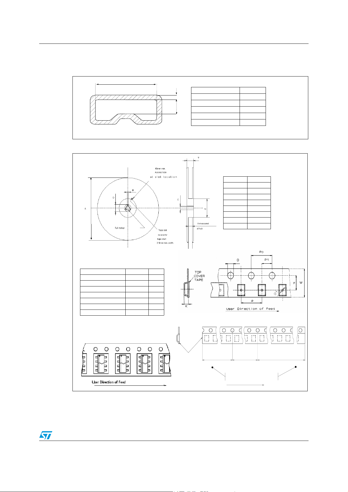
4.3 SO-8 Packing information
Figure 31. SO-8 tube shipment (no suffix)
B
C
Base Q.ty 100
Bulk Q.ty 2000
Tube length (± 0.5) 532
A
A 3.2
B 6
C (± 0.1) 0.6
All dimensions are in mm.
Figure 32. SO-8 tape and reel shipment (suffix “TR”)
TAPE DIMENSIONS
According to Electronic Industries Association
(EIA) Standard 481 rev. A, Feb. 1986
Tape width W 12
Tape Hole Spacing P0 (± 0.1) 4
Component Spacing P 8
Hole Diameter D (± 0.1/-0) 1.5
Hole Diameter D1 (min) 1.5
Hole Position F (± 0.05) 5.5
Compartment Depth K (max) 4.5
Hole Spacing P1 (± 0.1) 2
All dimensions are in mm.
End
REEL DIMENSIONS
Base Q.ty 2500
Bulk Q.ty 2500
A (max) 330
B (min) 1.5
C (± 0.2) 13
F 20.2
G (+ 2 / -0) 12.4
N (min) 60
T (max) 18.4
All dimensions are in mm.
Start
Top
cover
tape
500mm min
Empty components pockets
saled with cover tape.
User direction of feed
No componentsNo components Components
500mm min
19/21
Page 20

Revision history VNS3NV04D-E
5 Revision history
Table 10. Document revision history
Date Revision Changes
28-Oct-2005 1 Initial release.
02-Jul-2007 2
Document reformatted and converted into new ST template.
Tab l e 4: O ff - I
unit corrected
DSS
20/21
Page 21

VNS3NV04D-E
Please Read Carefully:
Information in this document is provided solely in connection with ST products. STMicroelectronics NV and its subsidiaries (“ST”) reserve the
right to make changes, corrections, modifications or improvements, to this document, and the products and services described herein at any
time, without notice.
All ST products are sold pursuant to ST’s terms and conditions of sale.
Purchasers are solely responsible for the choice, selection and use of the ST products and services described herein, and ST assumes no
liability whatsoever relating to the choice, selection or use of the ST products and services described herein.
No license, express or implied, by estoppel or otherwise, to any intellectual property rights is granted under this document. If any part of this
document refers to any third party products or services it shall not be deemed a license grant by ST for the use of such third party products
or services, or any intellectual property contained therein or considered as a warranty covering the use in any manner whatsoever of such
third party products or services or any intellectual property contained therein.
UNLESS OTHERWISE SET FORTH IN ST’S TERMS AND CONDITIONS OF SALE ST DISCLAIMS ANY EXPRESS OR IMPLIED
WARRANTY WITH RESPECT TO THE USE AND/OR SALE OF ST PRODUCTS INCLUDING WITHOUT LIMITATION IMPLIED
WARRANTIES OF MERCHANTABILITY, FITNESS FOR A PARTICULAR PURPOSE (AND THEIR EQUIVALENTS UNDER THE LAWS
OF ANY JURISDICTION), OR INFRINGEMENT OF ANY PATENT, COPYRIGHT OR OTHER INTELLECTUAL PROPERTY RIGHT.
UNLESS EXPRESSLY APPROVED IN WRITING BY AN AUTHORIZED ST REPRESENTATIVE, ST PRODUCTS ARE NOT
RECOMMENDED, AUTHORIZED OR WARRANTED FOR USE IN MILITARY, AIR CRAFT, SPACE, LIFE SAVING, OR LIFE SUSTAINING
APPLICATIONS, NOR IN PRODUCTS OR SYSTEMS WHERE FAILURE OR MALFUNCTION MAY RESULT IN PERSONAL INJURY,
DEATH, OR SEVERE PROPERTY OR ENVIRONMENTAL DAMAGE. ST PRODUCTS WHICH ARE NOT SPECIFIED AS "AUTOMOTIVE
GRADE" MAY ONLY BE USED IN AUTOMOTIVE APPLICATIONS AT USER’S OWN RISK.
Resale of ST products with provisions different from the statements and/or technical features set forth in this document shall immediately void
any warranty granted by ST for the ST product or service described herein and shall not create or extend in any manner whatsoever, any
liability of ST.
ST and the ST logo are trademarks or registered trademarks of ST in various countries.
Information in this document supersedes and replaces all information previously supplied.
The ST logo is a registered trademark of STMicroelectronics. All other names are the property of their respective owners.
© 2007 STMicroelectronics - All rights reserved
STMicroelectronics group of companies
Australia - Belgium - Brazil - Canada - China - Czech Republic - Finland - France - Germany - Hong Kong - India - Israel - Italy - Japan -
Malaysia - Malta - Morocco - Singapore - Spain - Sweden - Switzerland - United Kingdom - United States of America
www.st.com
21/21
 Loading...