

Page 1

Features
VNL5050N3-E
VNL5050S5-E
OMNIFET III
fully protected low-side driver
Typ e V
VNL5050N3-E
VNL5050S5-E
■ Drain current: 19 A
■ ESD protection
■ Overvoltage clamp
■ Thermal shutdown
■ Current and power limitation
■ Very low standby current
■ Very low electromagnetic susceptibility
■ In compliance with the 2002/95/EC european
clamp
41 V 50 mΩ 19 A
R
DS(on)
I
D
directive
■ Open drain status output
(a)
2
3
2
1
SOT-223
SO-8
Description
The VNL5050N3-E and VNL5050S5-E are
monolithic devices made using
STMicroelectronics VIPower Technology,
intended for driving resistive or inductive loads
with one side connected to the battery. Built-in
thermal shutdown protects the chip from
overtemperature and short-circuit. Output current
limitation protects the devices in an overload
condition. In case of long duration overload, the
device limits the dissipated power to a safe level
up to thermal shutdown intervention.Thermal
shutdown, with automatic restart, allows the
device to recover normal operation as soon as a
fault condition disappears. Fast demagnetization
of inductive loads is achieved at turn-off.
a. Valid for VNL5050S5-E only
Table 1. Devices summary
Package
SOT-223 VNL5050N3-E VNL5050N3TR-E
SO-8 VNL5050S5-E VNL5050S5TR-E
November 2009 Doc ID 15917 Rev 4 1/32
Order codes
Tube Tape & reel
www.st.com
1
Page 2

Contents VNL5050N3-E / VNL5050S5-E
Contents
1 Block diagrams and pins configurations . . . . . . . . . . . . . . . . . . . . . . . . 5
2 Absolute maximum rating . . . . . . . . . . . . . . . . . . . . . . . . . . . . . . . . . . . . 8
2.1 Absolute maximum ratings . . . . . . . . . . . . . . . . . . . . . . . . . . . . . . . . . . . . . 8
2.2 Thermal data . . . . . . . . . . . . . . . . . . . . . . . . . . . . . . . . . . . . . . . . . . . . . . . 8
3 Electrical characteristics . . . . . . . . . . . . . . . . . . . . . . . . . . . . . . . . . . . . . 9
3.1 Electrical characteristics curves . . . . . . . . . . . . . . . . . . . . . . . . . . . . . . . . 12
3.2 MCU I/O protection . . . . . . . . . . . . . . . . . . . . . . . . . . . . . . . . . . . . . . . . . . 17
4 Package and PC board thermal data . . . . . . . . . . . . . . . . . . . . . . . . . . . 18
4.1 SOT-223 thermal data . . . . . . . . . . . . . . . . . . . . . . . . . . . . . . . . . . . . . . . 18
4.2 SO-8 thermal data . . . . . . . . . . . . . . . . . . . . . . . . . . . . . . . . . . . . . . . . . . 21
5 Package and packing information . . . . . . . . . . . . . . . . . . . . . . . . . . . . . 24
5.1 ECOPACK® . . . . . . . . . . . . . . . . . . . . . . . . . . . . . . . . . . . . . . . . . . . . . . . 24
5.2 SOT-223 mechanical data . . . . . . . . . . . . . . . . . . . . . . . . . . . . . . . . . . . . 24
5.3 SO-8 mechanical data . . . . . . . . . . . . . . . . . . . . . . . . . . . . . . . . . . . . . . . 26
5.4 SOT-223 packing information . . . . . . . . . . . . . . . . . . . . . . . . . . . . . . . . . . 28
5.5 SO-8 packing information . . . . . . . . . . . . . . . . . . . . . . . . . . . . . . . . . . . . . 29
6 Revision history . . . . . . . . . . . . . . . . . . . . . . . . . . . . . . . . . . . . . . . . . . . 30
2/32 Doc ID 15917 Rev 4
Page 3

VNL5050N3-E / VNL5050S5-E List of tables
List of tables
Table 1. Devices summary . . . . . . . . . . . . . . . . . . . . . . . . . . . . . . . . . . . . . . . . . . . . . . . . . . . . . . . . . 1
Table 2. Pin function . . . . . . . . . . . . . . . . . . . . . . . . . . . . . . . . . . . . . . . . . . . . . . . . . . . . . . . . . . . . . . 6
Table 3. Suggested connections for unused and n.c. pins . . . . . . . . . . . . . . . . . . . . . . . . . . . . . . . . . 7
Table 4. Absolute maximum ratings . . . . . . . . . . . . . . . . . . . . . . . . . . . . . . . . . . . . . . . . . . . . . . . . . . 8
Table 5. Thermal data . . . . . . . . . . . . . . . . . . . . . . . . . . . . . . . . . . . . . . . . . . . . . . . . . . . . . . . . . . . . . 8
Table 6. Power MOS section . . . . . . . . . . . . . . . . . . . . . . . . . . . . . . . . . . . . . . . . . . . . . . . . . . . . . . . 9
Table 7. Source drain diode . . . . . . . . . . . . . . . . . . . . . . . . . . . . . . . . . . . . . . . . . . . . . . . . . . . . . . . . 9
Table 8. Input section. . . . . . . . . . . . . . . . . . . . . . . . . . . . . . . . . . . . . . . . . . . . . . . . . . . . . . . . . . . . . 9
Table 9. Status pin . . . . . . . . . . . . . . . . . . . . . . . . . . . . . . . . . . . . . . . . . . . . . . . . . . . . . . . . . . . . . . . 9
Table 10. Logic input . . . . . . . . . . . . . . . . . . . . . . . . . . . . . . . . . . . . . . . . . . . . . . . . . . . . . . . . . . . . . 10
Table 11. Openload detection. . . . . . . . . . . . . . . . . . . . . . . . . . . . . . . . . . . . . . . . . . . . . . . . . . . . . . . 10
Table 12. Supply section . . . . . . . . . . . . . . . . . . . . . . . . . . . . . . . . . . . . . . . . . . . . . . . . . . . . . . . . . . 10
Table 13. Switching characteristics . . . . . . . . . . . . . . . . . . . . . . . . . . . . . . . . . . . . . . . . . . . . . . . . . . 11
Table 14. Protection and diagnostics . . . . . . . . . . . . . . . . . . . . . . . . . . . . . . . . . . . . . . . . . . . . . . . . . 11
Table 15. Truth table. . . . . . . . . . . . . . . . . . . . . . . . . . . . . . . . . . . . . . . . . . . . . . . . . . . . . . . . . . . . . . 14
Table 16. Thermal parameters . . . . . . . . . . . . . . . . . . . . . . . . . . . . . . . . . . . . . . . . . . . . . . . . . . . . . . 20
Table 17. Thermal parameters . . . . . . . . . . . . . . . . . . . . . . . . . . . . . . . . . . . . . . . . . . . . . . . . . . . . . . 23
Table 18. SOT-223 mechanical data . . . . . . . . . . . . . . . . . . . . . . . . . . . . . . . . . . . . . . . . . . . . . . . . . 25
Table 19. SO-8 mechanical data . . . . . . . . . . . . . . . . . . . . . . . . . . . . . . . . . . . . . . . . . . . . . . . . . . . . 27
Table 20. Document revision history . . . . . . . . . . . . . . . . . . . . . . . . . . . . . . . . . . . . . . . . . . . . . . . . . 30
Doc ID 15917 Rev 4 3/32
Page 4

List of figures VNL5050N3-E / VNL5050S5-E
List of figures
Figure 1. VNL5050N3-E block diagram . . . . . . . . . . . . . . . . . . . . . . . . . . . . . . . . . . . . . . . . . . . . . . . . 5
Figure 2. VNL5050S5-E block diagram . . . . . . . . . . . . . . . . . . . . . . . . . . . . . . . . . . . . . . . . . . . . . . . 5
Figure 3. VNL5050N3-E current and voltage conventions. . . . . . . . . . . . . . . . . . . . . . . . . . . . . . . . . . 6
Figure 4. VNL5050S5-E current and voltage conventions . . . . . . . . . . . . . . . . . . . . . . . . . . . . . . . . . 6
Figure 5. Configuration diagrams (top view) . . . . . . . . . . . . . . . . . . . . . . . . . . . . . . . . . . . . . . . . . . . . 7
Figure 6. Source diode forward characteristics . . . . . . . . . . . . . . . . . . . . . . . . . . . . . . . . . . . . . . . . . 12
Figure 7. Static drain source on-resistance vs. drain current. . . . . . . . . . . . . . . . . . . . . . . . . . . . . . . 12
Figure 8. Static drain source on-resistance vs. input voltage . . . . . . . . . . . . . . . . . . . . . . . . . . . . . . 12
Figure 9. Static drain source on-resistance vs. drain current. . . . . . . . . . . . . . . . . . . . . . . . . . . . . . . 12
Figure 10. Transfer characteristics . . . . . . . . . . . . . . . . . . . . . . . . . . . . . . . . . . . . . . . . . . . . . . . . . . . 13
Figure 11. Transfer characteristics (inside view for V
Figure 12. Output characteristics . . . . . . . . . . . . . . . . . . . . . . . . . . . . . . . . . . . . . . . . . . . . . . . . . . . . . 13
Figure 13. Normalized on-resistance vs. temperature . . . . . . . . . . . . . . . . . . . . . . . . . . . . . . . . . . . . . 13
Figure 14. Normalized input threshold vs. temperature . . . . . . . . . . . . . . . . . . . . . . . . . . . . . . . . . . . . 14
Figure 15. Switching characteristics . . . . . . . . . . . . . . . . . . . . . . . . . . . . . . . . . . . . . . . . . . . . . . . . . . 15
Figure 16. VNL5050N3-E application schematic . . . . . . . . . . . . . . . . . . . . . . . . . . . . . . . . . . . . . . . . . 15
Figure 17. VNL5050S5-E application schematic . . . . . . . . . . . . . . . . . . . . . . . . . . . . . . . . . . . . . . . . 16
Figure 18. Maximum demagnetization energy
Figure 19. SOT-223 PC board
(1)
. . . . . . . . . . . . . . . . . . . . . . . . . . . . . . . . . . . . . . . . . . . . . . . . . . . . . 18
(1)
Figure 20. Rthj-amb vs. PCB copper area in open box free air condition . . . . . . . . . . . . . . . . . . . . . . 18
Figure 21. SOT-223 thermal impedance junction ambient single pulse. . . . . . . . . . . . . . . . . . . . . . . . 19
Figure 22. Thermal fitting model of a LSD in SOT-223
Figure 23. SO-8 PC board
(1)
. . . . . . . . . . . . . . . . . . . . . . . . . . . . . . . . . . . . . . . . . . . . . . . . . . . . . . . . 21
Figure 24. Rthj-amb vs. PCB copper area in open box free air condition . . . . . . . . . . . . . . . . . . . . . . 21
Figure 25. SO-8 thermal impedance junction ambient single pulse. . . . . . . . . . . . . . . . . . . . . . . . . . . 22
Figure 26. Thermal fitting model of a LSD in SO-8
Figure 27. SOT-223 package dimensions . . . . . . . . . . . . . . . . . . . . . . . . . . . . . . . . . . . . . . . . . . . . . . 24
Figure 28. SO-8 package dimensions . . . . . . . . . . . . . . . . . . . . . . . . . . . . . . . . . . . . . . . . . . . . . . . . . 26
Figure 29. SOT-223 tape and reel shipment (suffix “TR”) . . . . . . . . . . . . . . . . . . . . . . . . . . . . . . . . . . 28
Figure 30. SO-8 tube shipment (no suffix) . . . . . . . . . . . . . . . . . . . . . . . . . . . . . . . . . . . . . . . . . . . . . . 29
Figure 31. SO-8 tape and reel shipment (suffix “TR”) . . . . . . . . . . . . . . . . . . . . . . . . . . . . . . . . . . . . . 29
= 2 V to 3 V) . . . . . . . . . . . . . . . . . . . . . . . . . 13
IN
. . . . . . . . . . . . . . . . . . . . . . . . . . . . . . . . . . . . . . . . . 17
(1)
. . . . . . . . . . . . . . . . . . . . . . . . . . . . . . . . . . 19
(1)
. . . . . . . . . . . . . . . . . . . . . . . . . . . . . . . . . . . . . 22
4/32 Doc ID 15917 Rev 4
Page 5

VNL5050N3-E / VNL5050S5-E Block diagrams and pins configurations
1 Block diagrams and pins configurations
Figure 1. VNL5050N3-E block diagram
Drain
Control & DiagnosticLOGIC
IN
DRIVER
(ACTIVE POWER LIMITATION)
Figure 2. VNL5050S5-E block diagram
SUPPLY
SUPPLY
LOGIC
Control & Diagnostic
OFF State
Open load
Current
Limitation
OVERTEMPERATURE
PROTECTION
OVERLOAD PROTECTION
Power
Clamp
GND
Drain
IN
ST
Current
Limitation
DRIVER
OVERTEMPERATURE
PROTECTION
OVERLOAD PROTECTION
(ACTIVE POWER LIMITATION)
Power
Clamp
GND
Doc ID 15917 Rev 4 5/32
Page 6

Block diagrams and pins configurations VNL5050N3-E / VNL5050S5-E
Table 2. Pin function
Name Function
INPUT
Voltage controlled input pin with hysteresis, CMOS compatible. Controls output
switch state
(1)
DRAIN Power MOS drain
SOURCE Power MOS source and ground reference for the control section
SUPPLY
VOLTAGE
STATUS Open drain digital diagnostic pin
1. Internally connected to V
2. Valid for VNL5050S5-E only.
Supply voltage connected to the signal part (5 V)
(2)
in the VNL5050N3-E
supply
Figure 3. VNL5050N3-E current and voltage conventions
Figure 4. VNL5050S5-E current and voltage conventions
6/32 Doc ID 15917 Rev 4
Page 7
VNL5050N3-E / VNL5050S5-E Block diagrams and pins configurations
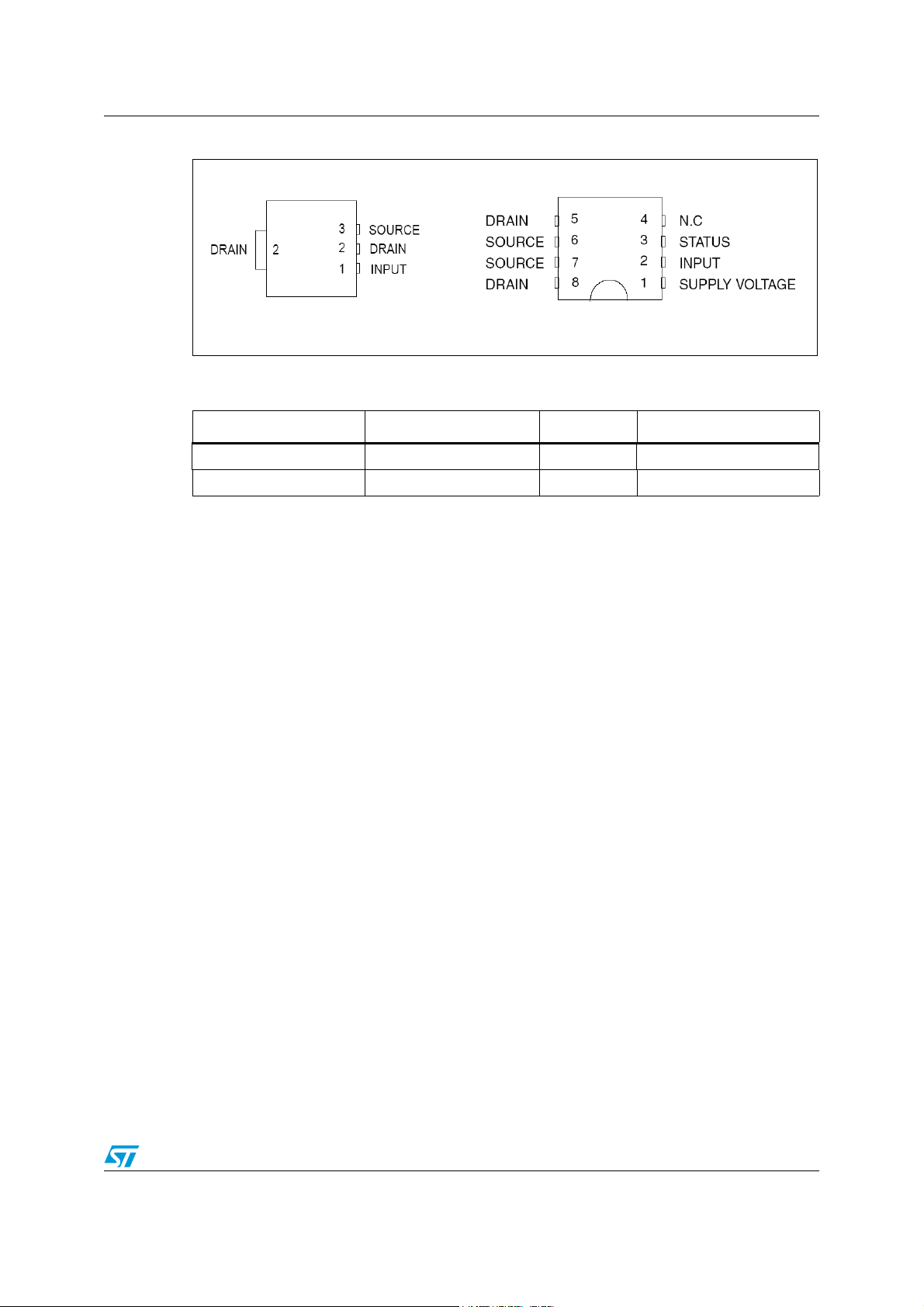
Figure 5. Configuration diagrams (top view)
SOT-223
Table 3. Suggested connections for unused and n.c. pins
SO-8
Connection / pin STATUS N.C. INPUT
Floating X X X
To ground Not allowed X Through 10 kΩ resistor
Doc ID 15917 Rev 4 7/32
Page 8
Absolute maximum rating VNL5050N3-E / VNL5050S5-E
2 Absolute maximum rating
Stressing the device above the rating listed in the Ta bl e 4 may cause permanent damage to
the device. These are stress ratings only and operation of the device at these or any other
conditions above those indicated in the operating sections of this specification is not implied.
Exposure to absolute maximum rating conditions for extended periods may affect device
reliability. Refer also to the STMicroelectronics SURE program and other relevant quality
document
2.1 Absolute maximum ratings
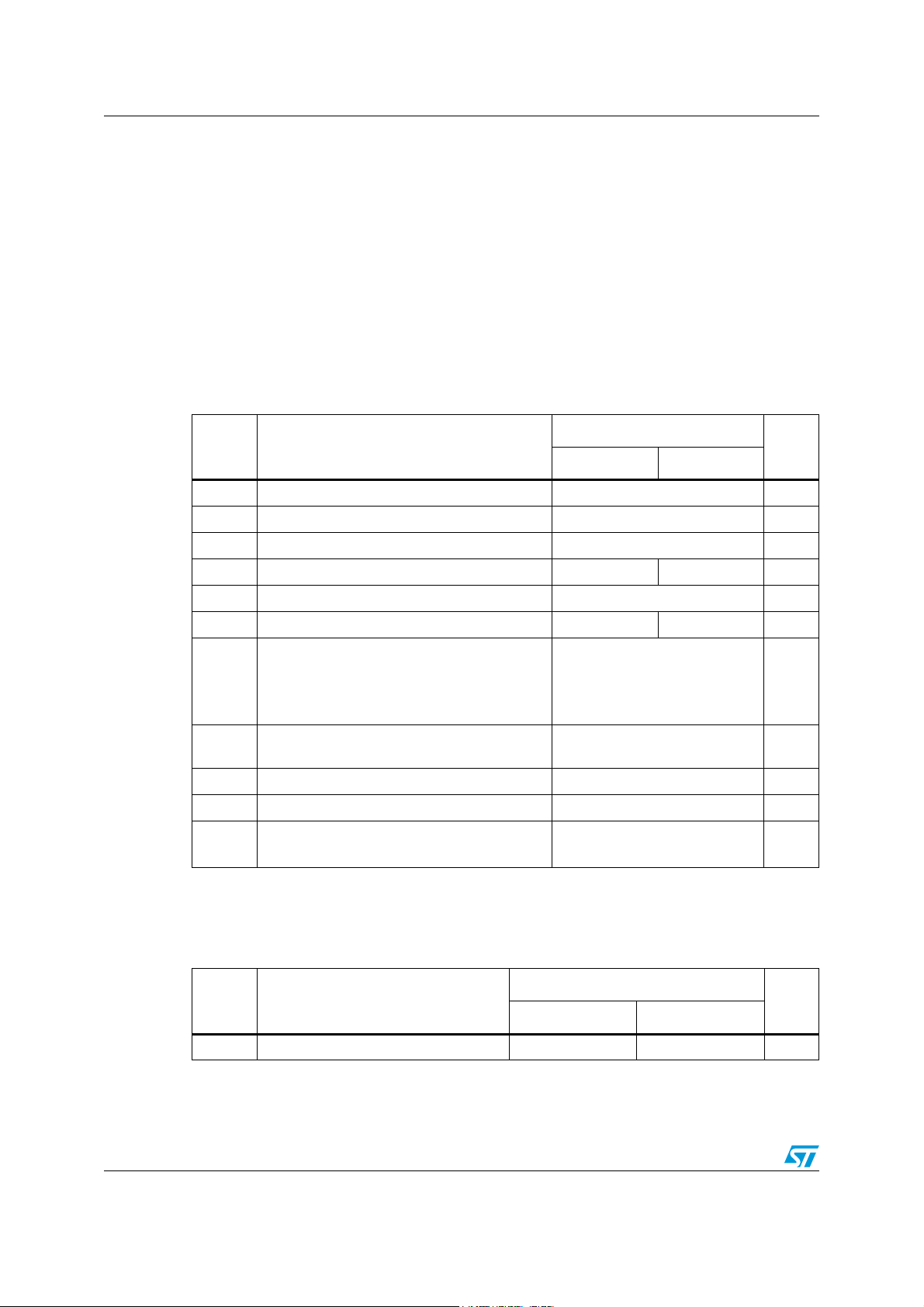
Table 4. Absolute maximum ratings
Val ue
Symbol Parameter
SOT-223 SO-8
Unit
V
- I
I
STAT
Drain-source voltage (V
DS
DC drain current Internally limited A
I
D
Reverse DC drain current -4 A
D
DC supply current - -1 to 10 mA
I
S
DC input current -1 to 10 mA
I
IN
DC status current - -1 to 10 mA
Electrostatic discharge
V
ESD1
(R = 1.5 kΩ; C = 100 pF)
– DRAIN
– SUPPLY, INPUT, STATUS
V
T
E
ESD2
Electrostatic discharge on output pin only
(R = 330 Ω, C = 150 pF)
Junction operating temperature -40 to 150 °C
T
j
Storage temperature -55 to 150 °C
stg
Single pulse avalanche energy
AS
(L = 1.1 mH, TJ= 150 °C, RL=0, I
2.2 Thermal data
= 0 V) Internally clamped V
IN
5000
4000
2000 V
OUT
= I
limL
)
93 mJ
V
Table 5. Thermal data
Symbol Parameter
R
thj-amb
1. When mounted on a standard single-sided FR4 board with 0.5 cm2 of Cu (at least 35 µm thick) connected
to all DRAIN pins
Thermal resistance junction-ambient 108.3
8/32 Doc ID 15917 Rev 4
Maximum value
SOT-223 SO-8
(1)
87 °C/W
Unit
Page 9
VNL5050N3-E / VNL5050S5-E Electrical characteristics
3 Electrical characteristics
Values specified in this section are for V
supply
= V
= 4.5 V to 5.5 V, -40 °C < Tj < 150 °C,
IN
unless otherwise stated.
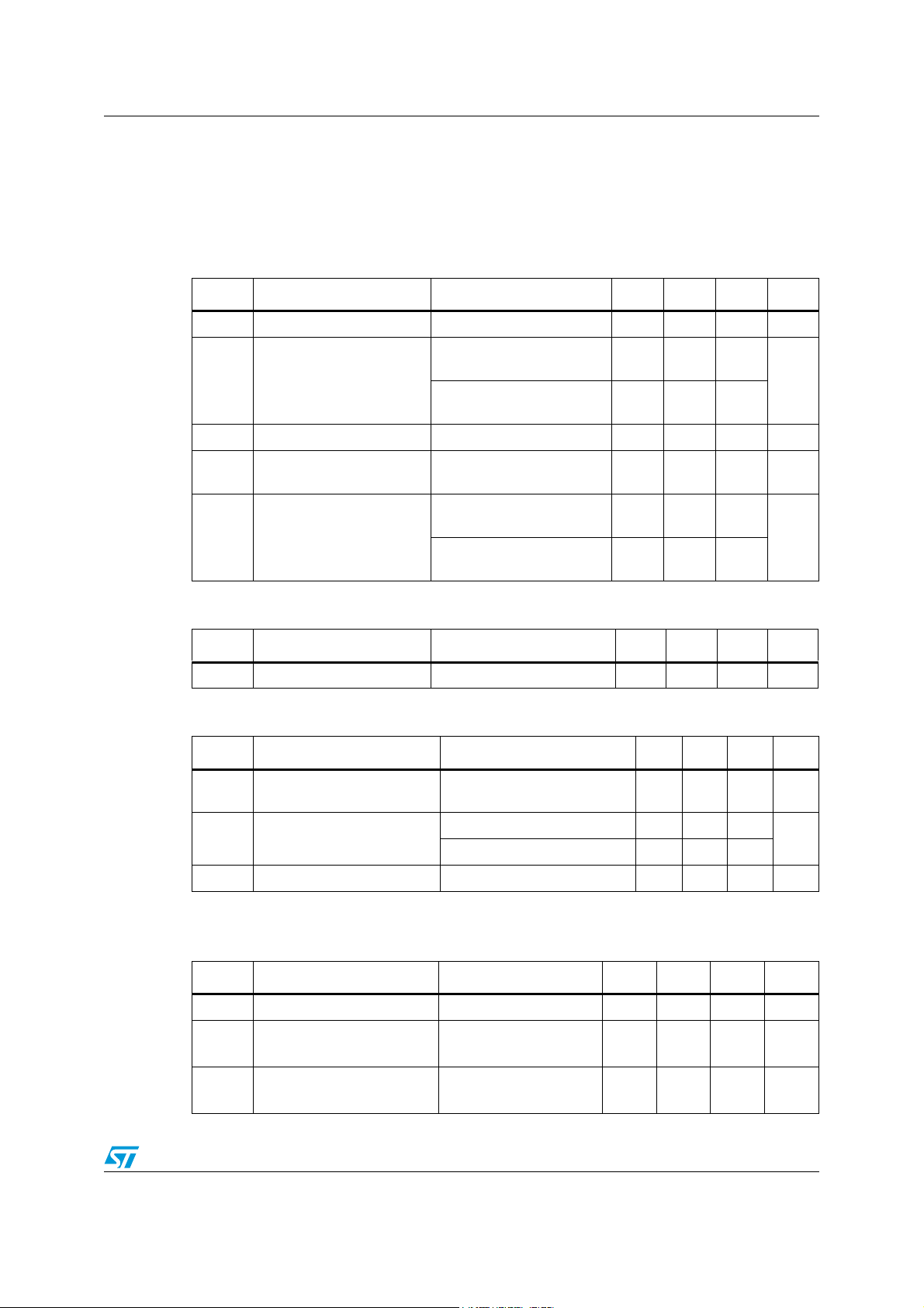
Table 6. Power MOS section
Symbol Parameter Test conditions Min. Typ. Max. Unit
V
R
V
CLAMP
V
I
Table 7. Source drain diode
Symbol Parameter Test conditions Min. Typ. Max. Unit
supply
ON
CLTH
DSS
Operating supply voltage - 3.5 5 5.5 V
I
= 2 A; Tj = 25 °C,
ON-state resistance
Drain-source clamp voltage V
Drain-source clamp
threshold voltage
D
= VIN = 5 V
V
supply
= 2 A; Tj = 150 °C,
I
D
V
= VIN = 5 V
supply
= 0 V; ID = 2 A 41 46 52 V
IN
= 0 V; ID = 2 mA 36 V
V
IN
V
= 0 V; V
IN
Tj = 25 °C
DS
= 13 V;
03
50
mΩ
100
OFF-state output current
V
= 0 V; V
IN
Tj = 125 °C
DS
= 13 V;
05
µA
V
Table 8. Input section
Forward on voltage ID = 2 A; V
SD
(1)
.
= 0 V - 0.8 - V
IN
Symbol Parameter Test conditions Min. Typ. Max. Unit
= V
I
Supply current from input pin
ISS
ON-state: V
= 0 V
V
DS
supply
= 5 V;
IN
30 110 µA
IS = 1 mA 5.5 7
V
V
1. Valid for VNL5050N3-E option (input and supply pins connected together)
Table 9. Status pin
Input clamp voltage
ICL
Input threshold voltage V
INTH
(1)
= -1 mA -0.7
I
S
= VIN; ID = 1 mA 1 3.5 V
DS
Symbol Parameter Test conditions Min. Typ. Max. Unit
V
STAT
I
LSTAT
C
STAT
Status low output voltage I
Status leakage current
Status pin input capacitance
= 1mA 0.5 V
STAT
Normal operation,
V
= 5 V
STAT
Normal operation,
V
= 5 V
STAT
10 µA
100 pF
V
Doc ID 15917 Rev 4 9/32
Page 10

Electrical characteristics VNL5050N3-E / VNL5050S5-E
Table 9. Status pin
(1)
(continued)
Symbol Parameter Test conditions Min. Typ. Max. Unit
I
= 1 mA 5.5 7
V
1. Valid for VNL5050S5-E option
Table 10. Logic input
Status clamp voltage
STCL
(1)
STAT
= -1 mA -0.7
I
STAT
V
Symbol Parameter Test conditions Min. Typ. Max. Unit
V
Low-level input voltage - 0.9 V
IL
Low-level input current V
I
IL
V
High-level input voltage - 2.1 V
IH
High-level input current V
I
IH
I(hyst)
ICL
Input hysteresis voltage - 0.13 V
Input clamp voltage
V
V
1. Valid for VNL5050S5-E option
Table 11. Openload detection
(1)
= 0.9 V 1 µA
IN
= 2.1 V 10 µA
IN
= 1 mA 5.5 7
I
IN
= -1 mA -0.7
I
IN
V
Symbol Parameter Test conditions Min. Typ. Max. Unit
Openload OFF-state voltage
V
Ol
detection threshold
V
= 0 V 0.6 1.2 1.7 V
IN
Delay between INPUT falling
t
d(oloff)
edge and STATUS falling edge
I
= 0 A 45 425 1100 µs
OUT
in openload condition
1. Valid for VNL5050S5-E option
Table 12. Supply section
(1)
Symbol Parameter Test conditions Min. Typ. Max. Unit
I
Supply current
S
V
1. Valid for VNL5050S5-E option
Supply clamp voltage
SCL
OFF-state: T
= V
V
IN
ON-state: T
V
= 5 V; V
IN
I
= 1 mA 5.5 7
SCL
= -1 mA -0.7
I
SCL
DRAIN
= 25 °C;
j
= 0 V;
= 25 °C;
j
= 0 V
DS
10 25
µA
25 110
V
10/32 Doc ID 15917 Rev 4
Page 11
VNL5050N3-E / VNL5050S5-E Electrical characteristics
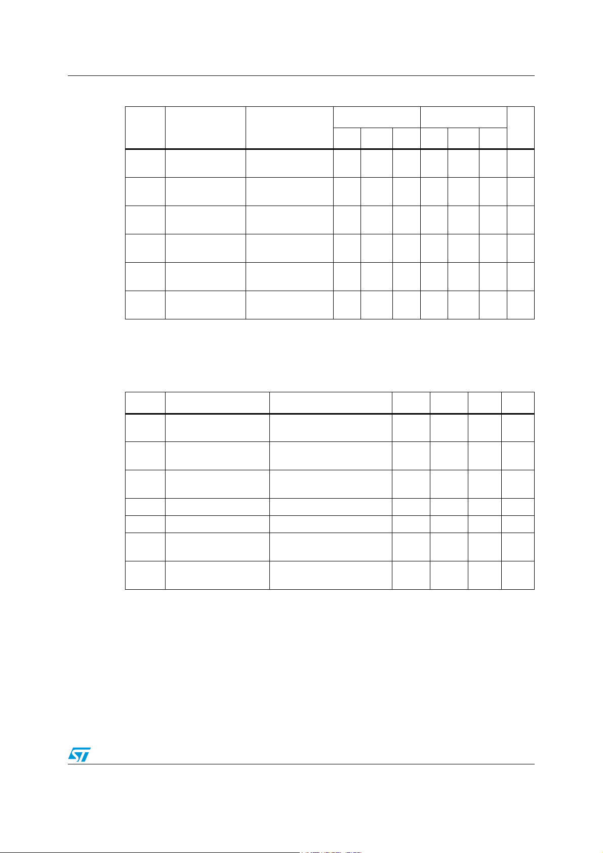
Table 13. Switching characteristics
(1)
SOT-223
(2)
SO-8
Symbol Parameter Test conditions
Min. Typ. Max Min. Typ. Max.
R
= 6.5 Ω,
t
d(ON)
t
d(OFF)
W
W
1. see Figure 16: VNL5050N3-E application schematic and Figure 17: VNL5050S5-E application schematic
2. 3.5 V ≤ V
3. See Figure 15: Switching characteristics
Table 14. Protection and diagnostics
Turn-on delay time
Turn-off delay time
t
Rise time
r
t
Fall time
f
Switching energy
ON
losses at turn-on
Switching energy
OFF
losses at turn-off
supply
= VIN ≤ 5.5 V
Symbol Parameter Test conditions
L
VCC = 13 V
= 6.5 Ω,
R
L
= 13 V
V
CC
= 6.5 Ω,
R
L
V
= 13 V
CC
R
= 6.5 Ω,
L
V
= 13 V
CC
RL = 6.5 Ω,
= 13 V
V
CC
RL = 6.5 Ω,
= 13 V
V
CC
(3)
-6--6 -µs
-20- -20-µs
- 10 - - 10 - µs
- 10 - - 10 - µs
-0.04- -0.04-mJ
-0.06- -0.06-mJ
(1)
Min. Typ. Max. Unit
Unit
limH
limL
dlimL
TSD
(2)
R
HYST
supply
DC short-circuit current
Short-circuit current
during thermal cycling
Step response current
limit
Shutdown temperature - 150 175 200 °C
Reset temperature - T
Thermal reset of
(3)
STATUS
Thermal hysteresis
- TR)
(T
TSD
= V
in VNL5050N3-E version
input
I
I
t
T
T
TRS
T
1. V
2. Valid for VNL5050S5-E option
= 13 V;
V
DS
V
= VIN=5V
supply
V
= 13 V; TR < Tj < T
DS
V
= VIN=5V
supply
= 13 V; V
V
DS
19 27 38 A
TSD;
= 5 V 44 µs
input
RS
11 A
+ 1 T
+ 5 °C
RS
- 135 °C
-7°C
Doc ID 15917 Rev 4 11/32
Page 12
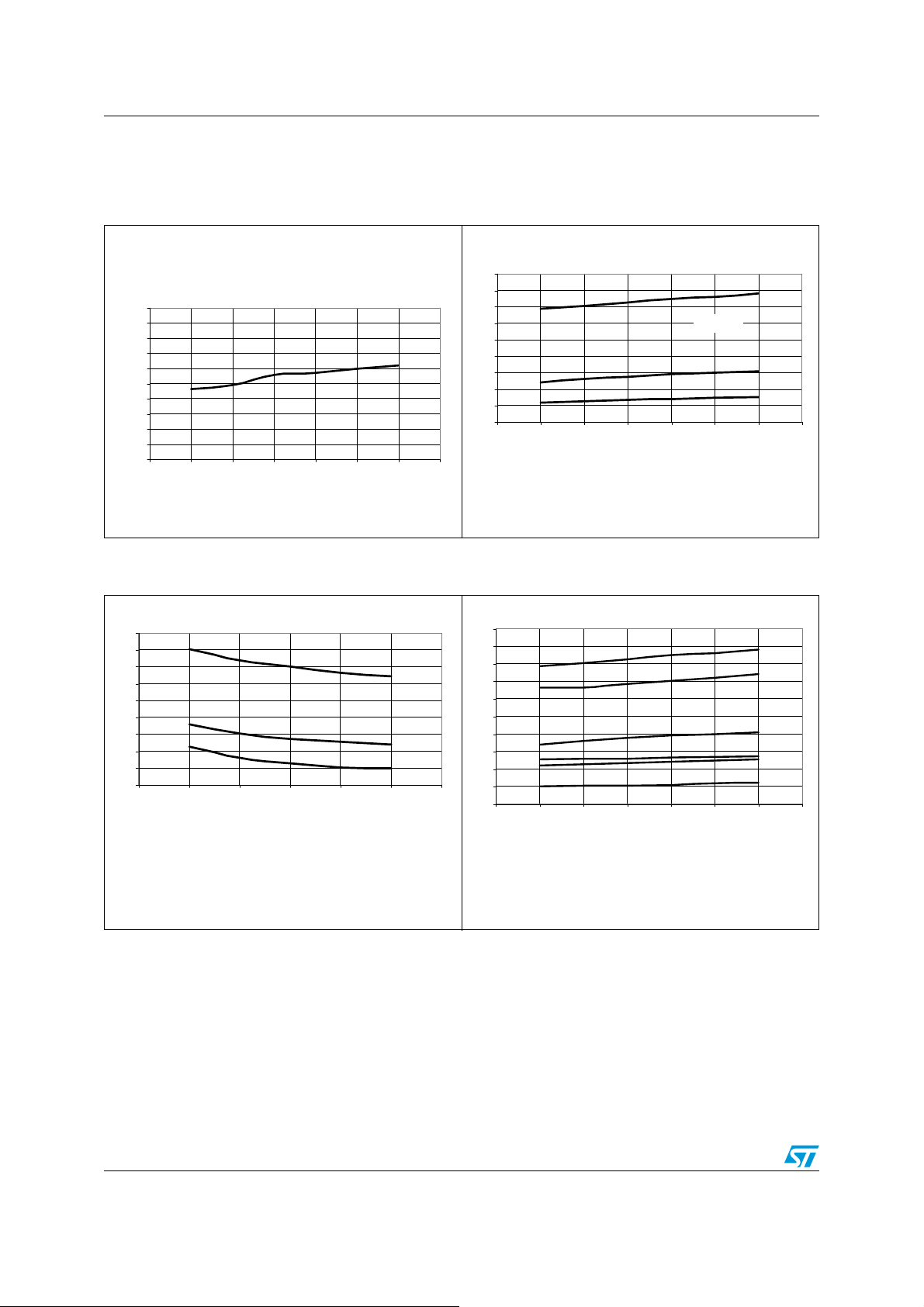
Electrical characteristics VNL5050N3-E / VNL5050S5-E
3.1 Electrical characteristics curves
Figure 6. Source diode forward
characteristics
Vf (mV)
1000
950
900
850
800
750
700
650
600
550
500
012345 67
Id (A)
Figure 8. Static drain source on-resistance
vs. input voltage
RON (mΩ)
110
100
90
80
70
60
50
40
30
20
33.544.555.56
I
D
= 3 A
A: Tj = -40 °C B: Tj = 25 °C C: Tj = 150 °C
Note: Input and supply pins connected together
C
B
A
VIN (V)
Figure 7. Static drain source on-resistance
vs. drain current
RON (mΩ)
120
110
100
90
80
70
60
50
40
30
0123 4567
C
VIN = 3.5 V
B
A
ID (A)
= -40 °C B: Tj = 25 °C C: Tj = 150 °C
A: T
j
Note: Input and supply pins connected together
Figure 9. Static drain source on-resistance
vs. drain current
R
(mΩ )
DS(on)
120
110
100
90
80
70
60
50
40
30
20
01234567
A : Vin = 3.5 V, Tj = 150 °C
B : Vin = 5 V, Tj = 150 °C
C : Vin = 3.5 V, Tj = 25 °C
Note: Input and supply pins connected together
A
B
C
D
F
Id (A)
E
D : Vin = 5 V, Tj = 25 °C
E : Vin = 3.5 V, Tj = -40 °C
F : Vin = 5 V, Tj = -40 °C
12/32 Doc ID 15917 Rev 4
Page 13
VNL5050N3-E / VNL5050S5-E Electrical characteristics
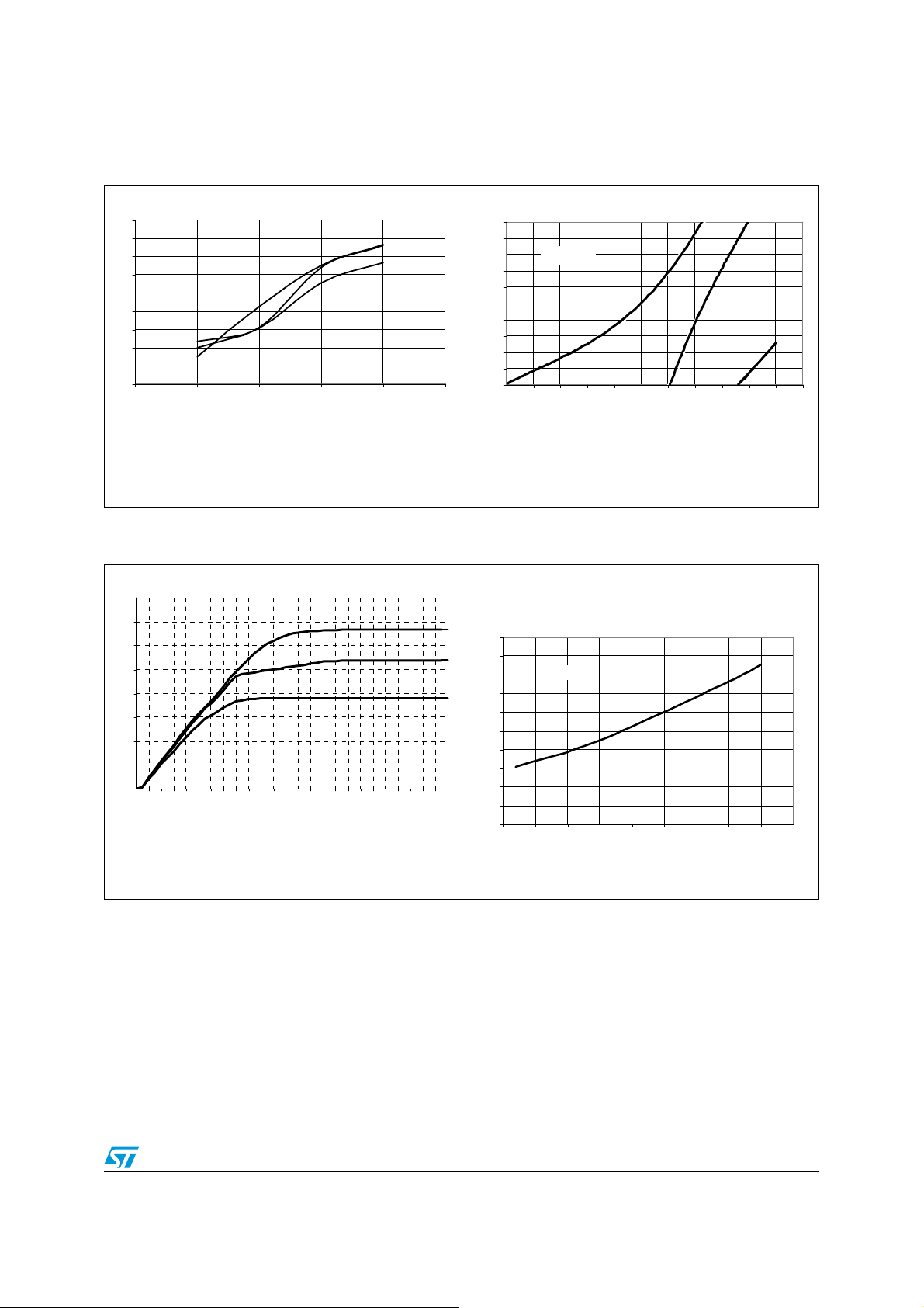
Figure 10. Transfer characteristics Figure 11. Transfer characteristics (inside
ID (A)
36
34
32
30
28
26
24
22
20
18
33.544.555.5
= 13 V
V
DS
A
B
B
C
A
C
VIN (V)
A: T
= -40 °C B: Tj = 25 °C C: Tj = 150 °C
j
Note: Input and supply pins connected together
view for V
ID (mA)
5000
4500
4000
3500
3000
2500
2000
1500
1000
500
0
A: Tj = -40 °C B: Tj = 25 °C C: Tj = 150 °C
Note: Input and supply pins connected together
VDS = 13 V
C
2 2.1 2.2 2.3 2.4 2.5 2.6 2.7 2.8 2.9 3 3.1
= 2V to 3V)
IN
B
VIN (V)
A
Figure 12. Output characteristics Figure 13. Normalized on-resistance vs.
temperature
ID (A)
40.0
35.0
30.0
25.0
20.0
15.0
10.0
5.0
0.0
0.0 0.3 0.6 0.9 1.3 1.9 2.7 3.8 4.9 6.1 7.3 8.3 9.5
A
B
C
VDS (V)
A: VIN = 5 V B: VIN = 4V C: VIN = 3 V
Note: Input and supply pins connected together
Ron (mΩ)
100
90
80
70
60
50
40
30
20
10
0
-50 -25 0 25 50 75 100 125 150 175
Iout = 2 A
Tj (° C)
Doc ID 15917 Rev 4 13/32
Page 14
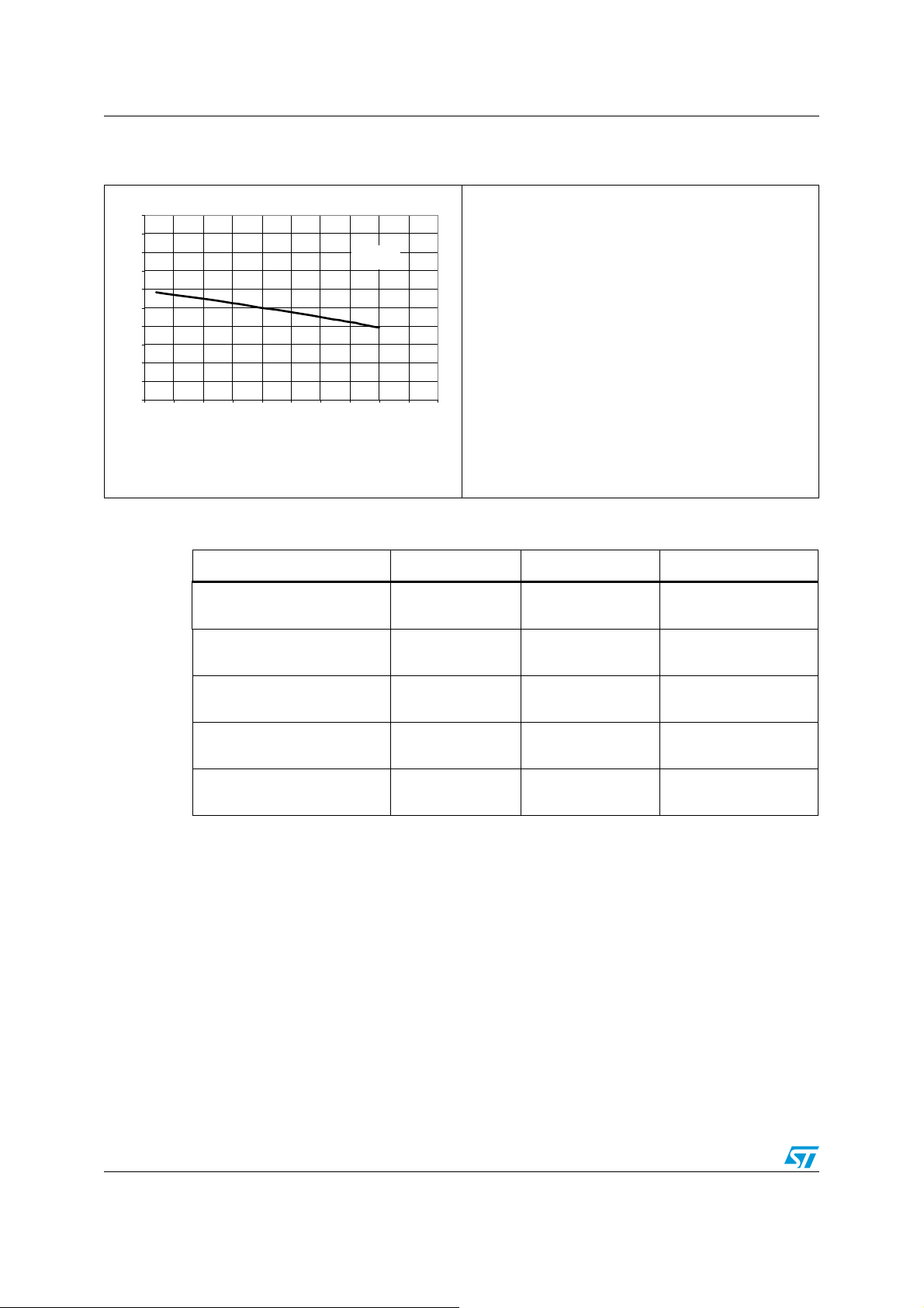
Electrical characteristics VNL5050N3-E / VNL5050S5-E
Figure 14. Normalized input threshold vs.
temperature
Vinth (V)
5
4.5
4
3.5
3
2.5
2
1.5
1
0.5
0
-50 -25 0 25 50 75 100 125 150 175 200
Tj ( °C)
Note: Input and supply pins connected together
Table 15. Truth table
Conditions INPUT DRAIN STATUS
Id = 1 mA
(1)
Normal operation
Current limitation
Overtemperature
Undervoltage
Output voltage < V
1.
Valid for VNL5050S5-E option
OL
L
H
L
H
L
H
L
H
L
H
H
L
H
X
H
H
H
H
L
L
H
H
H
H
H
L
X
X
L
H
14/32 Doc ID 15917 Rev 4
Page 15
VNL5050N3-E / VNL5050S5-E Electrical characteristics
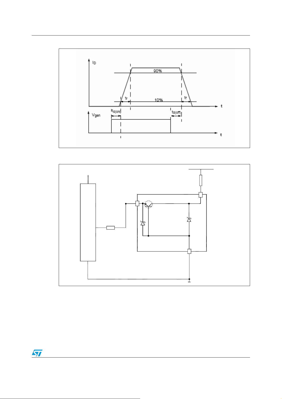
Figure 15. Switching characteristics
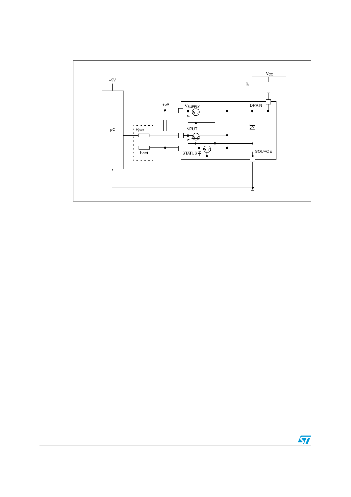
Figure 16. VNL5050N3-E application schematic
V
+5V
R
L
cc
µC
INPUT
R
prot
DRAIN
SOURCE
Doc ID 15917 Rev 4 15/32
Page 16
Electrical characteristics VNL5050N3-E / VNL5050S5-E
Figure 17. VNL5050S5-E application schematic
16/32 Doc ID 15917 Rev 4
Page 17
VNL5050N3-E / VNL5050S5-E Electrical characteristics
(
)
3.2 MCU I/O protection
ST suggests to insert a resistor (R
latching up
(a)
. The value of these resistors is a compromise between the leakage current of
prot
microcontroller and the current required by the LSD I/Os (input levels compatibility) with the
latch-up limit of microcontroller I/Os:
Equation 1
70
.
I
latchup
Let:
● I
● V
● 35 Ω ≤ R
Then, the recommended value is R
latchup
OHµC
> 20 mA
> 4.5 V
≤ 100 KΩ
prot
prot
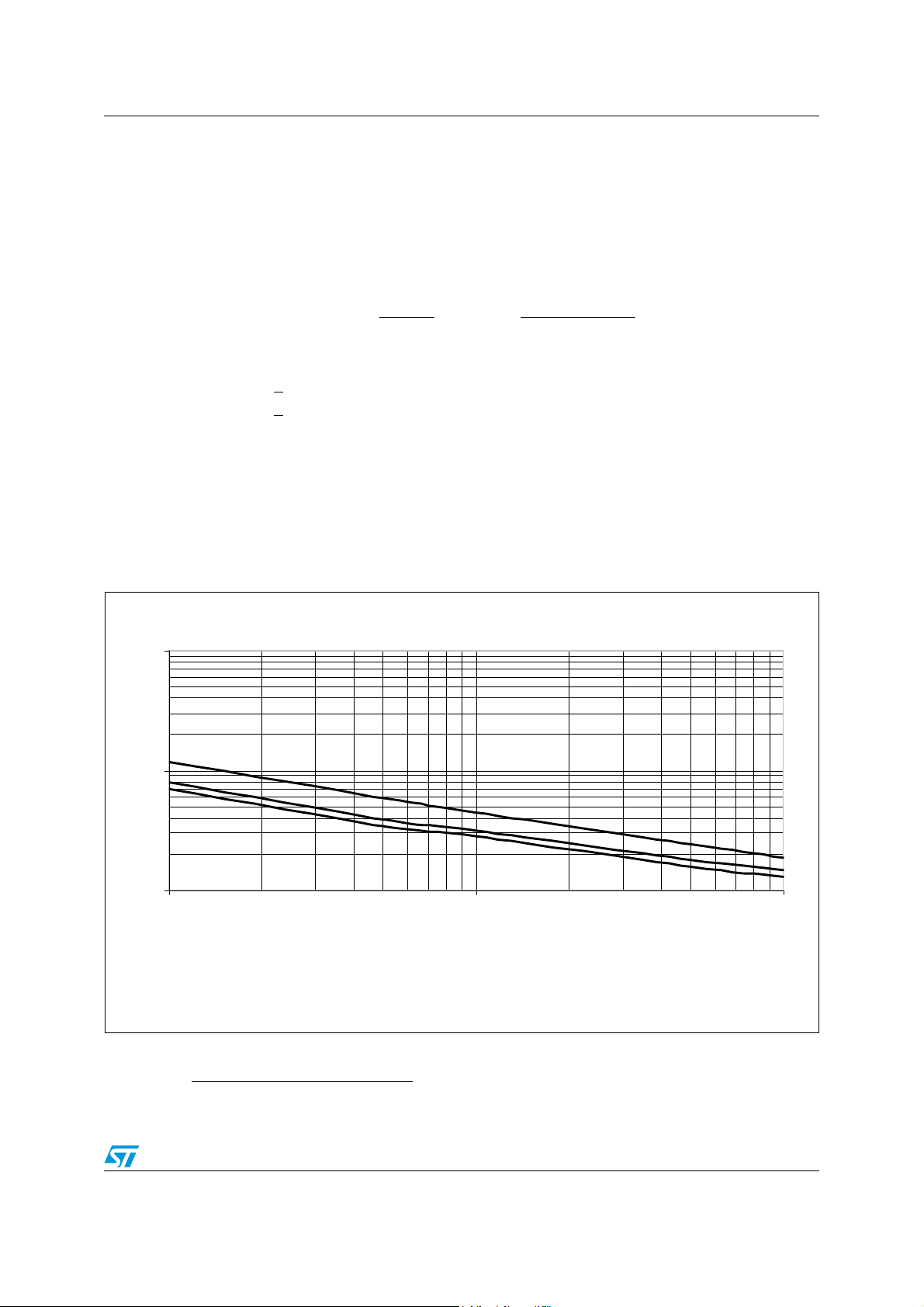
Figure 18 shows the turn-off current drawn during the demagnetization.
Figure 18. Maximum demagnetization energy
I (A )
) in line to prevent the microcontroller I/O pins from
VV
−
R
prot
≤≤
μ
I
IHCOH
maxIH
= 10 KΩ
(1)
100
A
10
1
110100
A: VNL5050x - Single pulse
B: Repetitive pulse T
C: Repetitive pulse T
1. The voltage supply is V
= 13.5 V
CC
= 100 °C
J
= 125 °C
J
B
C
L (mH)
a. In case of negative transient on the drain pin
Doc ID 15917 Rev 4 17/32
Page 18
Package and PC board thermal data VNL5050N3-E / VNL5050S5-E
4 Package and PC board thermal data
4.1 SOT-223 thermal data
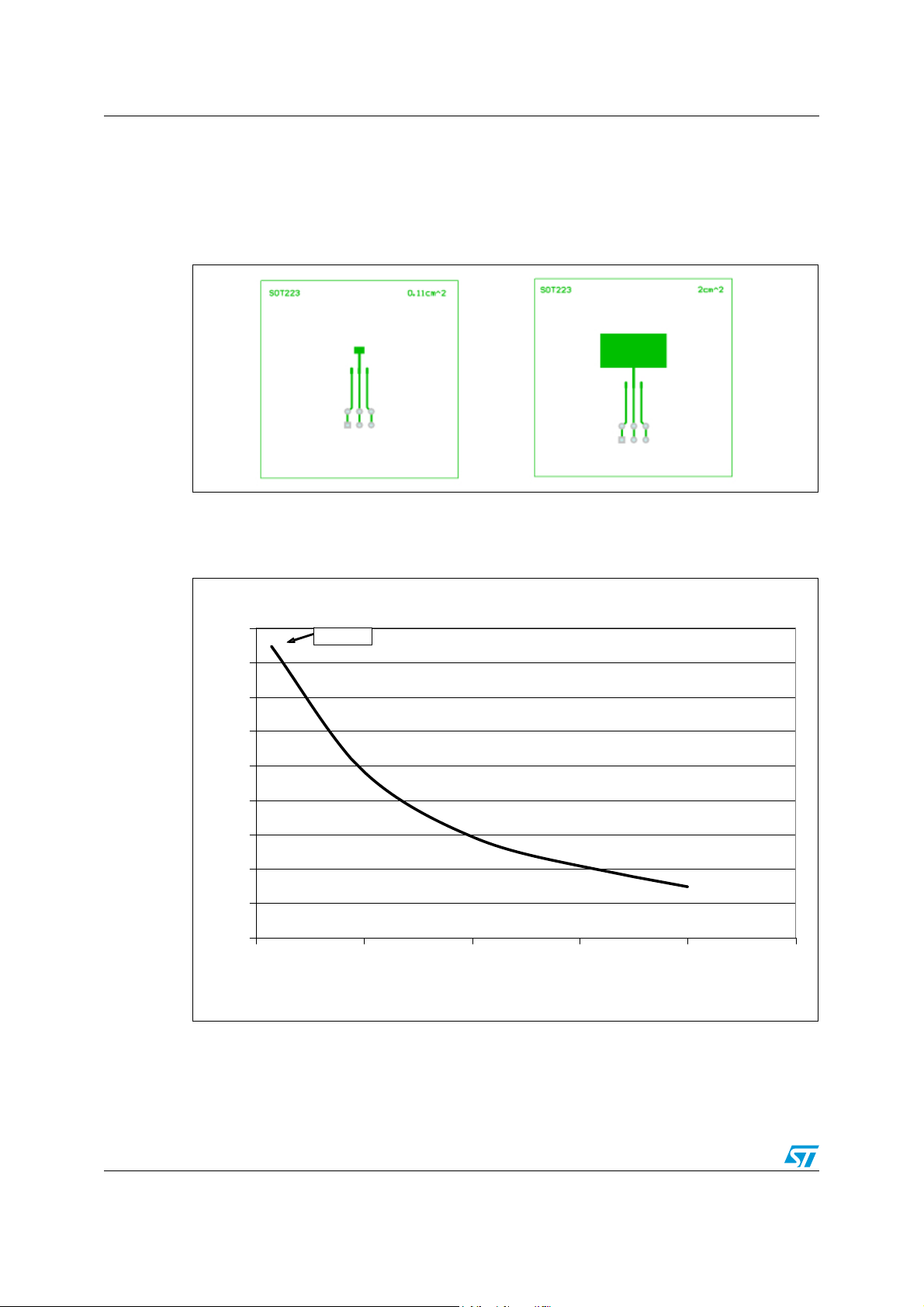
Figure 19. SOT-223 PC board
1. Layout condition of R
Cu thickness = 35 µm, copper areas: from minimum pad lay-out to 0.8 cm2).
Figure 20.
RTHjamb (°C/W)
RTHjamb (°C/W)
150
150
140
140
R
thj-amb
RTHj_amb(°C/W)
RTHj_amb(°C/W)
and Zth measurements (PCB FR4 area = 30 mm x 58 mm, PCB thickness = 2 mm,
th
vs. PCB copper area in open box free air condition
footprint
footprint
(1)
130
130
120
120
110
110
100
100
90
90
80
80
70
70
60
60
0 0.5 1 1.5 2 2.5
0 0.5 1 1.5 2 2.5
PCB Cu heatsink area (cm2)
PCB Cu heatsink area (cm2)
18/32 Doc ID 15917 Rev 4
Page 19
VNL5050N3-E / VNL5050S5-E Package and PC board thermal data
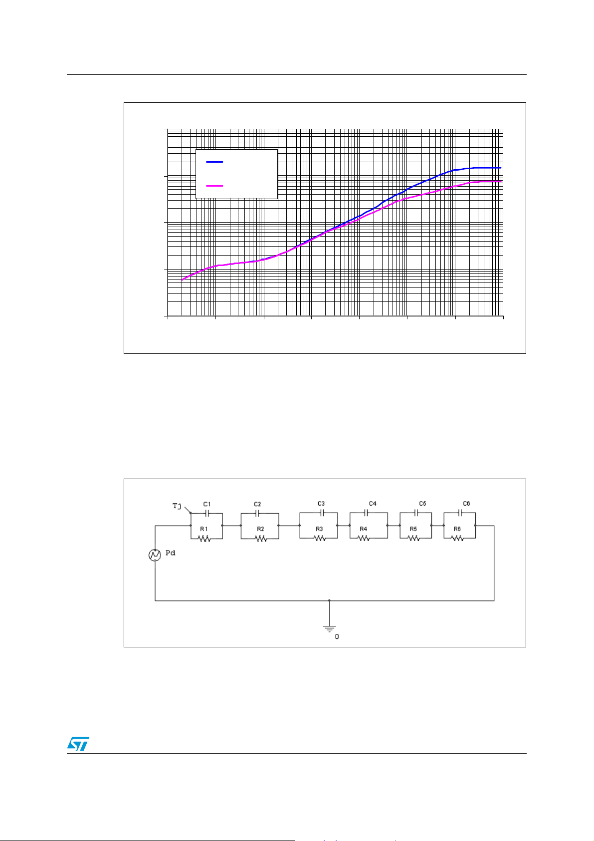
Figure 21. SOT-223 thermal impedance junction ambient single pulse
ZTH (°C/W)
1000
Cu footprint
100
10
1
0.1
0.0001 0.001 0.01 0.1 1 10 100 1000
Cu=2 cm2
Time (s)
Equation 2: pulse calculation formula
Z
THδ
δ Z
R
TH
THtp
1 δ–()+⋅=
where δ = tP/T
Figure 22. Thermal fitting model of a LSD in SOT-223
1. The fitting model is a semplified thermal tool and is valid for transient evolutions where the embedded
protections (power limitation or thermal cycling during thermal shutdown) are not triggered.
(1)
Doc ID 15917 Rev 4 19/32
Page 20
Package and PC board thermal data VNL5050N3-E / VNL5050S5-E
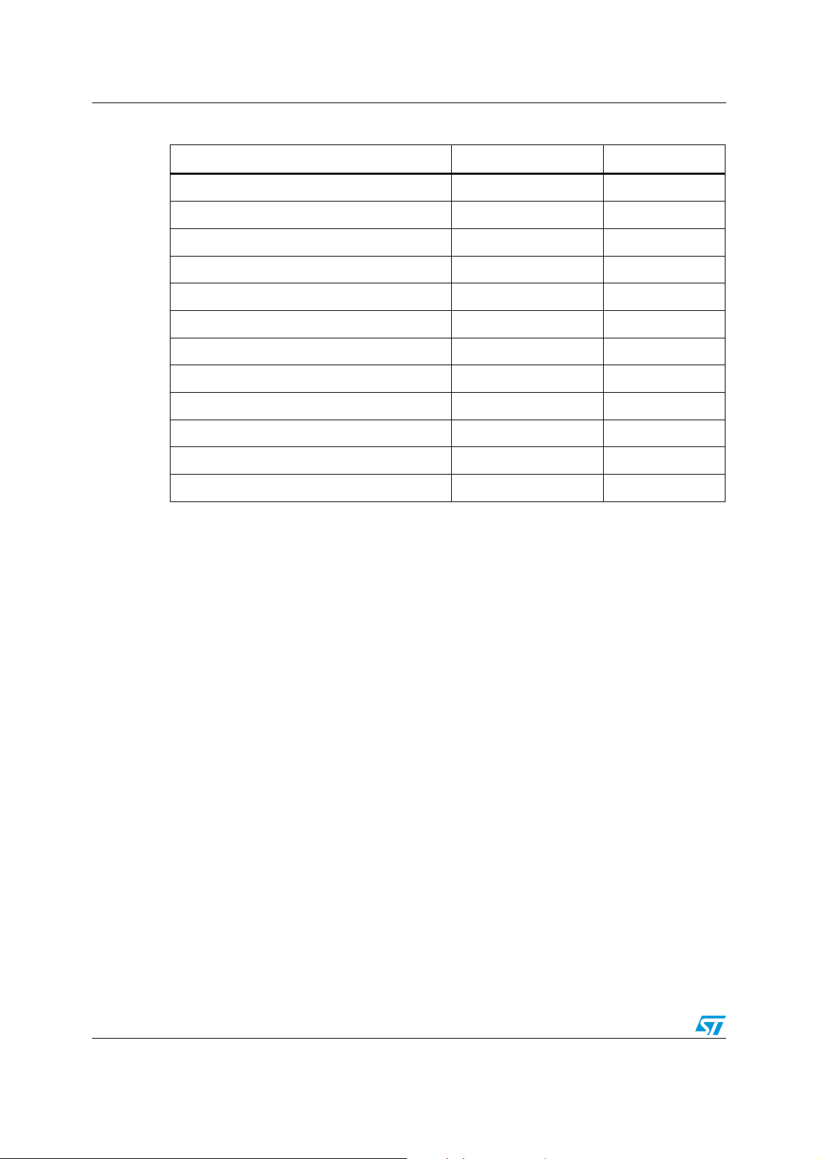
Table 16. Thermal parameters
Area/island (cm2)Footprint2
R1 (°C/W) 0.4
R2 (°C/W) 0.8
R3 (°C/W) 4.5
R4 (°C/W) 24
R5 (°C/W) 0.1
R6 (°C/W) 115 45
C1 (W.s/°C) 0.00006
C2 (W.s/°C) 0.0005
C3 (W.s/°C) 0.03
C4 (W.s/°C) 0.16
C5 (W.s/°C) 1000
C6 (W.s/°C) 0.4 2
20/32 Doc ID 15917 Rev 4
Page 21
VNL5050N3-E / VNL5050S5-E Package and PC board thermal data
4.2 SO-8 thermal data
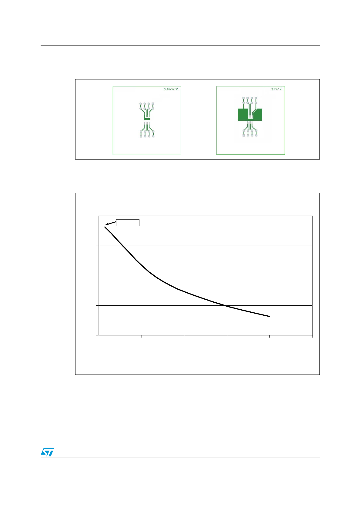
Figure 23. SO-8 PC board
1. Layout condition of R
Cu thickness = 35 µm (front and back side), Copper areas: from minimum pad lay-out to 2 cm
Figure 24.
105
105
95
95
R
thj-amb
RTHjamb (°C/W)
RTHjamb (°C/W)
RTHj_amb(°C/W)
RTHj_amb(°C/W)
and Zth measurements (PCB FR4 area = 58 mm x 58 mm, PCB thickness = 2 mm,
th
vs. PCB copper area in open box free air condition
footprint
footprint
(1)
2
).
85
85
75
75
65
65
00.511.522.5
00.511.522.5
PCB Cu heatsink area (cm2)
PCB Cu heatsink area (cm2)
Doc ID 15917 Rev 4 21/32
Page 22
Package and PC board thermal data VNL5050N3-E / VNL5050S5-E
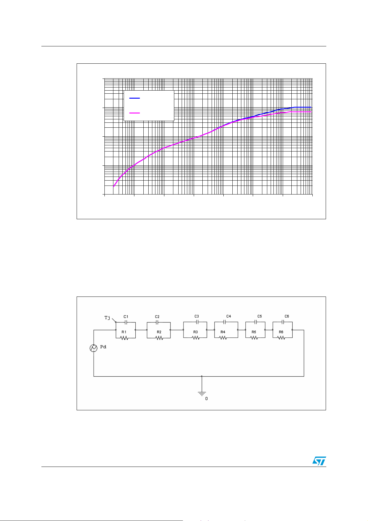
Figure 25. SO-8 thermal impedance junction ambient single pulse
ZTH (°C/W)
1000
Cu=footprint
100
Cu=2 cm2
10
1
0.1
0.0001 0.001 0.01 0.1 1 10 100 1000
Time (s)
Equation 3: pulse calculation formula
Z
THδ
δ Z
R
TH
THtp
1 δ–()+⋅=
where δ = tP/T
Figure 26. Thermal fitting model of a LSD in SO-8
(1)
1. The fitting model is a semplified thermal tool and is valid for transient evolutions where the embedded
protections (power limitation or thermal cycling during thermal shutdown) are not triggered.
22/32 Doc ID 15917 Rev 4
Page 23
VNL5050N3-E / VNL5050S5-E Package and PC board thermal data
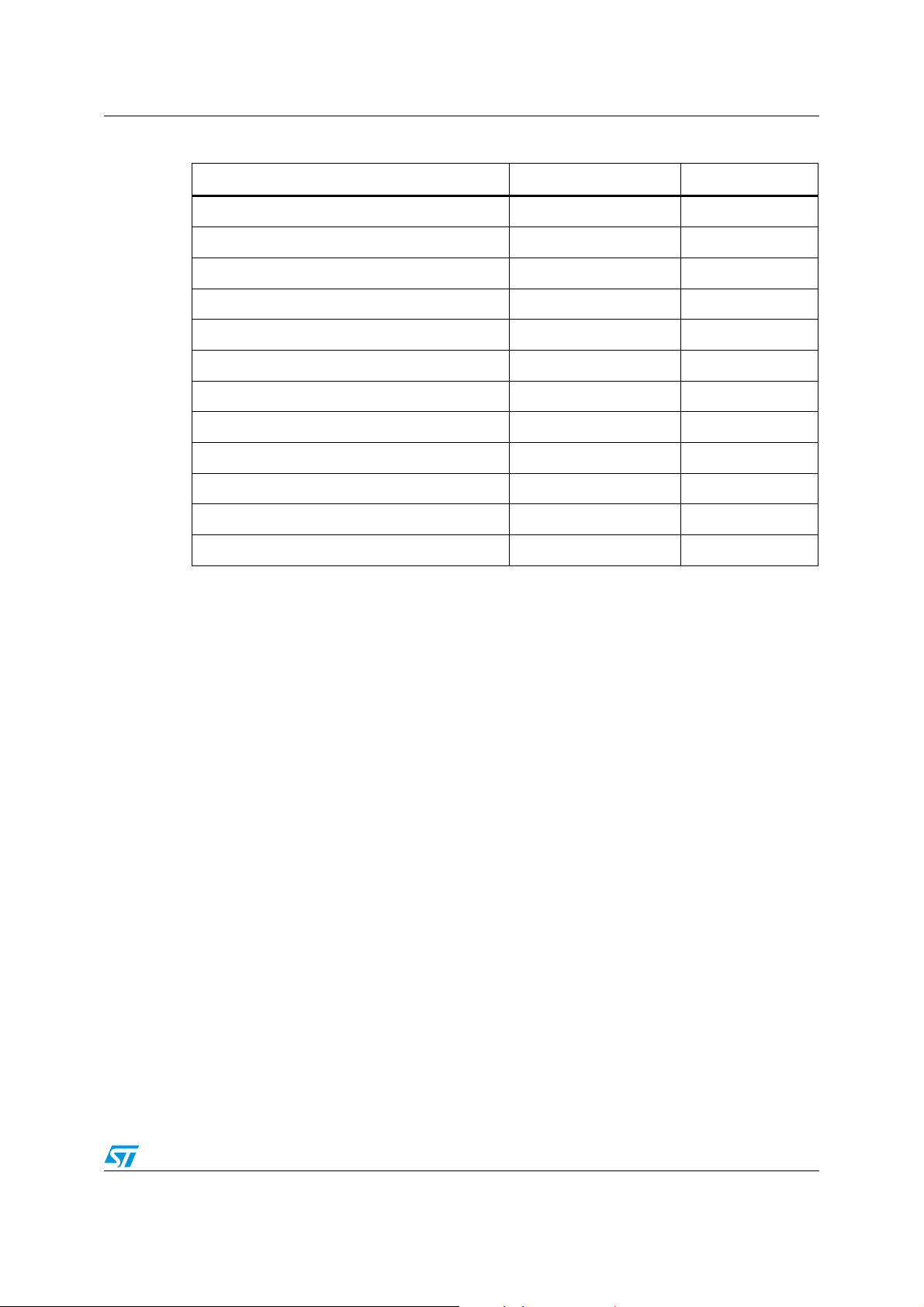
Table 17. Thermal parameters
Area/island (cm2)Footprint2
R1 (°C/W) 0.4
R2 (°C/W) 2.4
R3 (°C/W) 3.5
R4 (°C/W) 21
R5 (°C/W) 16
R6 (°C/W) 58 28
C1 (W.s/°C) 0.00008
C2 (W.s/°C) 0.0016
C3 (W.s/°C) 0.0075
C4 (W.s/°C) 0.045
C5 (W.s/°C) 0.35
C6 (W.s/°C) 1.05 2
Doc ID 15917 Rev 4 23/32
Page 24
Package and packing information VNL5050N3-E / VNL5050S5-E
5 Package and packing information
5.1 ECOPACK
In order to meet environmental requirements, ST offers these devices in different grades of
ECOPACK
specifications, grade definitions and product status are available at: www.st.com
ECOPACK
®
®
packages, depending on their level of environmental compliance. ECOPACK®
®
is an ST trademark.
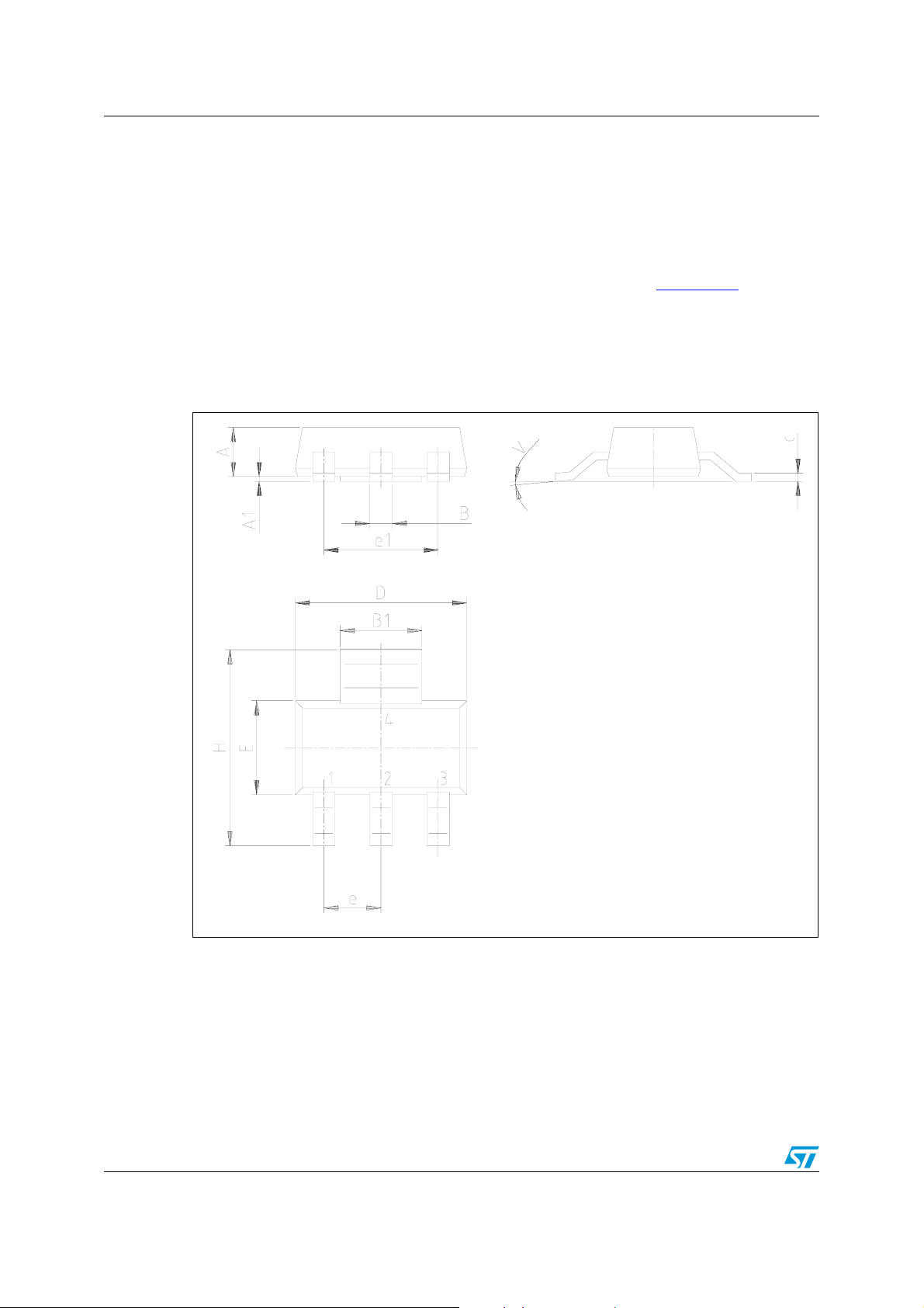
5.2 SOT-223 mechanical data
Figure 27. SOT-223 package dimensions
.
24/32 Doc ID 15917 Rev 4
0046067
Page 25
VNL5050N3-E / VNL5050S5-E Package and packing information
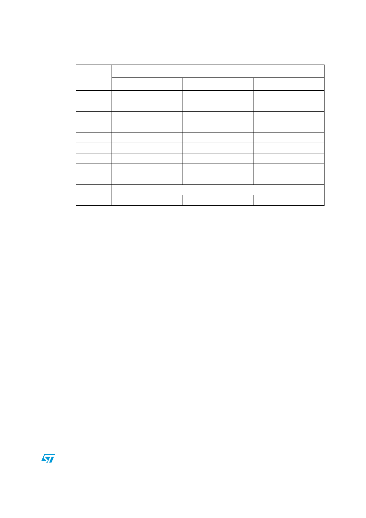
Table 18. SOT-223 mechanical data
mm. inch
DIM.
Min. Typ. Max. Min. Typ. Max.
A 1.8 0.071
B 0.6 0.7 0.85 0.024 0.027 0.033
B1 2.9 3 3.15 0.114 0.118 0.124
c 0.24 0.26 0.35 0.009 0.01 0.014
D 6.3 6.5 6.7 0.248 0.256 0.264
e 2.3 0.09
e1 4.6 0.181
E 3.3 3.5 3.7 0.13 0.138 0.146
H 6.7 7 7.3 0.264 0.276 0.287
V10 (max)
A1 0.02 0.1 0.0008 0.004
Doc ID 15917 Rev 4 25/32
Page 26
Package and packing information VNL5050N3-E / VNL5050S5-E
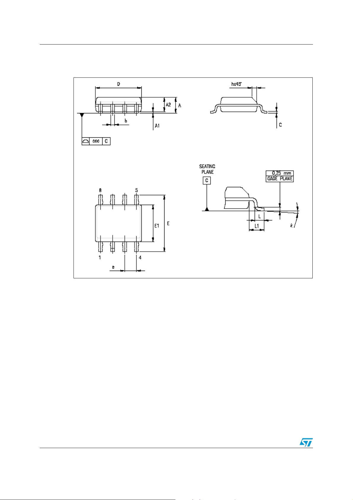
5.3 SO-8 mechanical data
Figure 28. SO-8 package dimensions
26/32 Doc ID 15917 Rev 4
Page 27
VNL5050N3-E / VNL5050S5-E Package and packing information
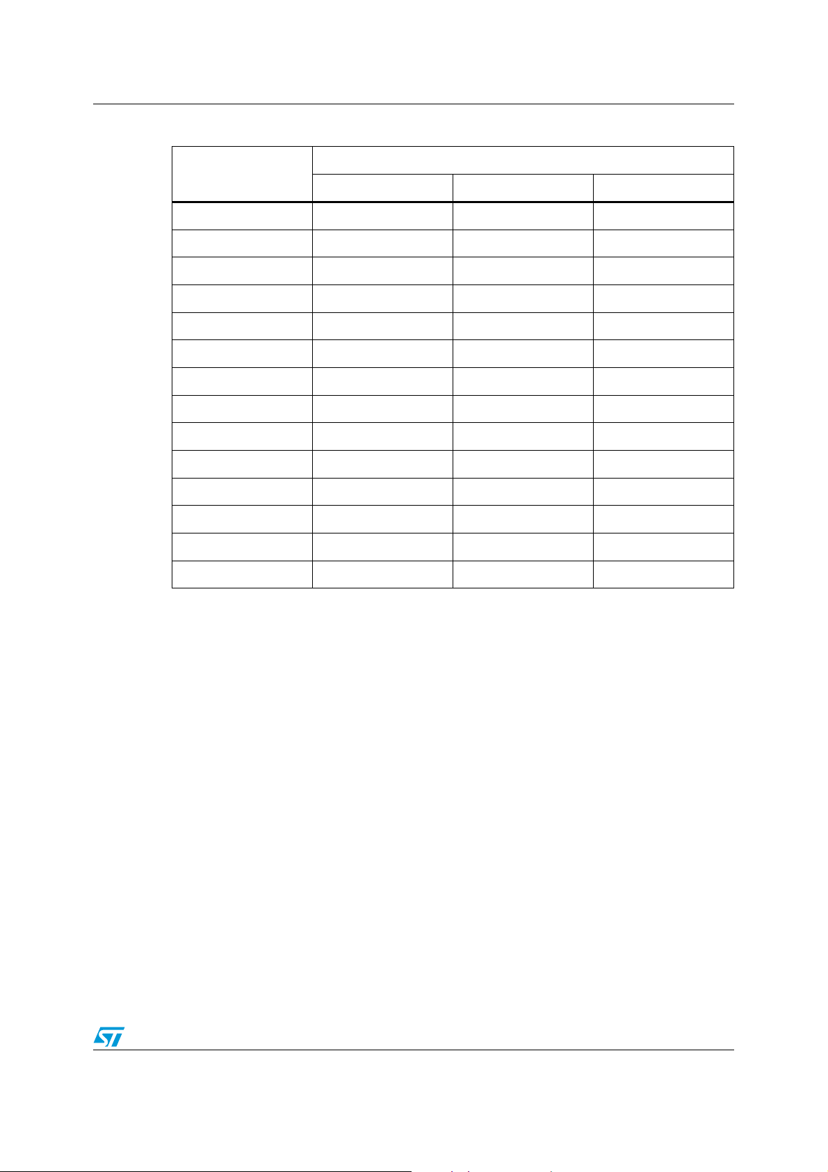
Table 19. SO-8 mechanical data
Symbol
Min. Typ. Max.
A 1.75
A1 0.10 0.25
A2 1.25
b 0.28 0.48
c 0.17 0.23
(1)
D
4.80 4.90 5.00
E 5.80 6.00 6.20
E1
(2)
3.80 3.90 4.00
e1.27
h 0.25 0.50
L 0.40 1.27
Millimeters
L1 1.04
k0° 8°
ccc 0.10
1. Dimensions D does not include mold flash, protrusions or gate burrs. Mold flash, potrusions or gate burrs
shall not exceed 0.15 mm in total (both side).
2. Dimension “E1” does not include interlead flash or protrusions. Interlead flash or protrusions shall not
exceed 0.25 mm per side.
Doc ID 15917 Rev 4 27/32
Page 28
Package and packing information VNL5050N3-E / VNL5050S5-E
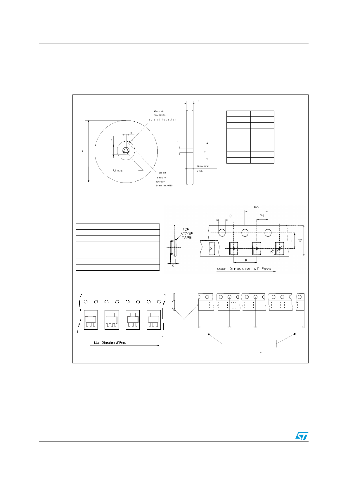
5.4 SOT-223 packing information
The devices can be packed in tube or tape and reel shipments (see the Table 1: Devices
summary on page 1 ).
Figure 29. SOT-223 tape and reel shipment (suffix “TR”)
Reel dimensions
Base Q.ty 1000
Bulk Q.ty 1000
A (max) 330
B (min) 1.5
C (± 0.2) 13
F 20.2
G (+ 2 / -0) 12.4
N (min) 60
T (max) 18.4
Tape dimensions
According to Electronic Industries Association
(EIA) Standard 481 rev. A, Feb. 1986
Tape width W 12
Tape Hole Spacing P0 (± 0.1) 4
Component Spacing P 8
Hole Diameter D (+ 0.1/-0) 1.5
Hole Diameter D1 (min) 1.5
Hole Position F (± 0.05) 5.5
Compartment Depth K (max) 4.5
Hole Spacing P1 (± 0.1) 2
All dimensions are in mm.
End
Top
cover
tape
28/32 Doc ID 15917 Rev 4
500mm min
Empty components pockets
saled with cover tape.
User direction of feed
Start
No componentsNo components Components
500mm min
Page 29
VNL5050N3-E / VNL5050S5-E Package and packing information
5.5 SO-8 packing information
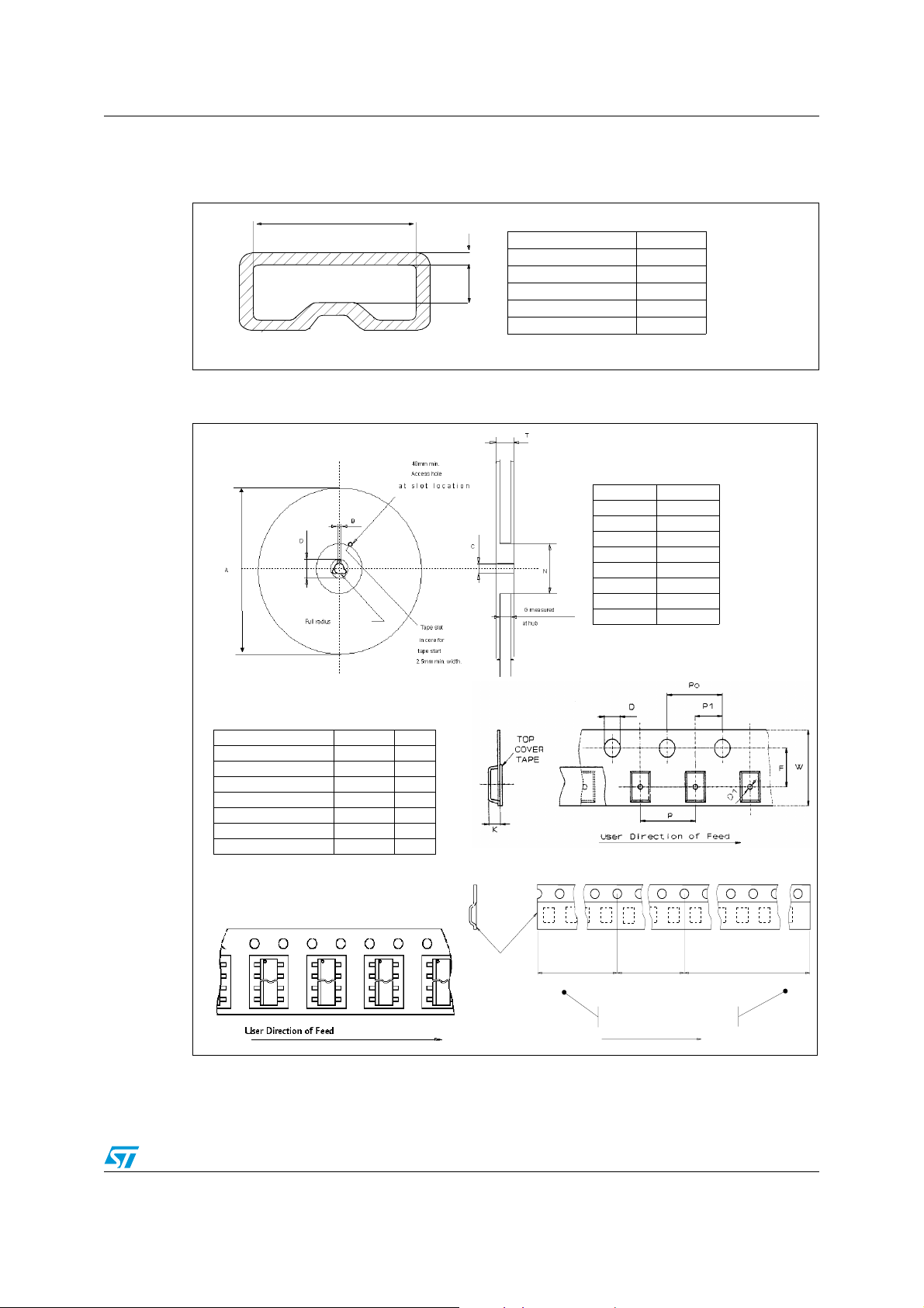
Figure 30. SO-8 tube shipment (no suffix)
B
C
Base q.ty 100
Bulk q.ty 2000
Tube length (± 0.5) 532
A
A 3.2
B 6
C (± 0.1) 0.6
All dimensions are in mm.
Figure 31. SO-8 tape and reel shipment (suffix “TR”)
Reel dimensions
Base q.ty 2500
Bulk q.ty 2500
A (max) 330
B (min) 1.5
C (± 0.2) 13
F 20.2
G (+ 2 / -0) 12.4
N (min) 60
T (max) 18.4
All dimensions are in mm.
Tape dimensions
According to Electronic Industries Association
(EIA) Standard 481 rev. A, Feb. 1986
Tape width W 12
Tape hole spacing P0 (± 0.1) 4
Component spacing P 8
Hole diameter D (+ 0.1/-0) 1.5
Hole diameter D1 (min) 1.5
Hole position F (± 0.05) 5.5
Compartment depth K (max) 4.5
Hole spacing P1 (± 0.1) 2
All dimensions are in mm.
Top
cover
tape
End
500mm min
Empty components pockets
saled with cover tape.
User direction of feed
Start
No componentsNo components Components
500mm min
Doc ID 15917 Rev 4 29/32
Page 30
Revision history VNL5050N3-E / VNL5050S5-E
6 Revision history
Table 20. Document revision history
Date Revision Changes
9-Jan-2008 1 Initial release.
Updated corporate template from V2 to V3
Table 3: Suggested connections for unused and n.c. pins
: updated parameter and value
ESD1
: changed value
ESD2
: deleted max value for SO-8
thj-case
: added max value for both SOT-223 and SO-8
thj-amb
: added typ value
SD
: added min/max value for IS = 1 mA
ICL
added min/max value
INTH:
: added max value for I
STCL
: added max value for IN = 1 mA
ICL
: changed unit of measurement for ON-state.
S
: added max value for I
VSL
: changed typ value both for SOT-223 and SO-8
d(OFF)
: added typ value for SO-8
ON
: added typ value for SO-8
OFF
: changed typ value
limL
: changed typ value
dlimL
valid for VNL5050N3-E option
R
STAT
STAT
= 1 mA
= 1 mA
25-Jun-2009 2
–V
–V
Table 4: Absolute maximum ratings
–R
–R
Table 7: Source drain diode
–V
Table 8: Input section.
–V
–V
Table 9: Status pin
–V
Table 10: Logic input
–V
Table 12: Supply section
–I
–V
Table 13: Switching characteristics
–t
–W
–W
– Added all typ column for SOT-223
Table 14: Protection and diagnostics
–I
–t
– Deleted row T
Added Figure 6: Source diode forward characteristics
Added Figure 7: Static drain source on-resistance vs. drain current
Added Figure 8: Static drain source on-resistance vs. input voltage
Added Figure 9: Static drain source on-resistance vs. drain current
Added Figure 10: Transfer characteristics
Added Figure 11: Output characteristics
Added Figure 12: Output characteristics
Added Figure 13: Normalized on-resistance vs. temperature
Added Chapter 4: Package and PC board thermal data
30/32 Doc ID 15917 Rev 4
Page 31
VNL5050N3-E / VNL5050S5-E Revision history
Table 20. Document revision history (continued)
Date Revision Changes
Deleted table 25: SOT-223 mechanical data & package outline
Added Figure 27: SOT-223 package dimensions
25-Jun-2009
(continued)
19-Aug-2009 3
20-Nov-2009 4
2
Added Table 18: SOT-223 mechanical data
Deleted table 26: SO-8 mechanical data & package outline
Added Figure 28: SO-8 package dimensions
Added Table 19: SO-8 mechanical data
Updated corporate template from V3 to V3-1
Deleted row for R
in Table 5: Thermal data
thj-case
Changed the document title
Took the first line off the bullet list for Features on cover page
Table 4: Absolute maximum ratings
–EAS: added new row
Table 6: Power MOS section
–V
: added new row
supply
–RON: updated test conditions
Table 8: Input section.
: updated test conditions
–I
SS
– Updated the table footnote
Table 13: Switching characteristics
– Moved footnote 2 and changed its text
: changed typ value
–W
ON
–W
: changed typ value
OFF
Table 14: Protection and diagnostics
: updated test conditions
–I
limH
: updated test conditions
–I
limL
: changed typ value
–t
dlimL
Updated Figure 7: Static drain source on-resistance vs. drain current
Updated Figure 8: Static drain source on-resistance vs. input voltage
Updated Figure 9: Static drain source on-resistance vs. drain current
Updated Figure 10: Transfer characteristics
Added Figure 11: Transfer characteristics (inside view for VIN = 2 V
to 3 V)
Updated Figure 14: Normalized input threshold vs. temperature
Added Section 3.2: MCU I/O protection
Doc ID 15917 Rev 4 31/32
Page 32

VNL5050N3-E / VNL5050S5-E
Please Read Carefully:
Information in this document is provided solely in connection with ST products. STMicroelectronics NV and its subsidiaries (“ST”) reserve the
right to make changes, corrections, modifications or improvements, to this document, and the products and services described herein at any
time, without notice.
All ST products are sold pursuant to ST’s terms and conditions of sale.
Purchasers are solely responsible for the choice, selection and use of the ST products and services described herein, and ST assumes no
liability whatsoever relating to the choice, selection or use of the ST products and services described herein.
No license, express or implied, by estoppel or otherwise, to any intellectual property rights is granted under this document. If any part of this
document refers to any third party products or services it shall not be deemed a license grant by ST for the use of such third party products
or services, or any intellectual property contained therein or considered as a warranty covering the use in any manner whatsoever of such
third party products or services or any intellectual property contained therein.
UNLESS OTHERWISE SET FORTH IN ST’S TERMS AND CONDITIONS OF SALE ST DISCLAIMS ANY EXPRESS OR IMPLIED
WARRANTY WITH RESPECT TO THE USE AND/OR SALE OF ST PRODUCTS INCLUDING WITHOUT LIMITATION IMPLIED
WARRANTIES OF MERCHANTABILITY, FITNESS FOR A PARTICULAR PURPOSE (AND THEIR EQUIVALENTS UNDER THE LAWS
OF ANY JURISDICTION), OR INFRINGEMENT OF ANY PATENT, COPYRIGHT OR OTHER INTELLECTUAL PROPERTY RIGHT.
UNLESS EXPRESSLY APPROVED IN WRITING BY AN AUTHORIZED ST REPRESENTATIVE, ST PRODUCTS ARE NOT
RECOMMENDED, AUTHORIZED OR WARRANTED FOR USE IN MILITARY, AIR CRAFT, SPACE, LIFE SAVING, OR LIFE SUSTAINING
APPLICATIONS, NOR IN PRODUCTS OR SYSTEMS WHERE FAILURE OR MALFUNCTION MAY RESULT IN PERSONAL INJURY,
DEATH, OR SEVERE PROPERTY OR ENVIRONMENTAL DAMAGE. ST PRODUCTS WHICH ARE NOT SPECIFIED AS "AUTOMOTIVE
GRADE" MAY ONLY BE USED IN AUTOMOTIVE APPLICATIONS AT USER’S OWN RISK.
Resale of ST products with provisions different from the statements and/or technical features set forth in this document shall immediately void
any warranty granted by ST for the ST product or service described herein and shall not create or extend in any manner whatsoever, any
liability of ST.
ST and the ST logo are trademarks or registered trademarks of ST in various countries.
Information in this document supersedes and replaces all information previously supplied.
The ST logo is a registered trademark of STMicroelectronics. All other names are the property of their respective owners.
© 2009 STMicroelectronics - All rights reserved
STMicroelectronics group of companies
Australia - Belgium - Brazil - Canada - China - Czech Republic - Finland - France - Germany - Hong Kong - India - Israel - Italy - Japan -
Malaysia - Malta - Morocco - Philippines - Singapore - Spain - Sweden - Switzerland - United Kingdom - United States of America
www.st.com
32/32 Doc ID 15917 Rev 4
 Loading...