

Page 1
VND05BSP
ISO HIGH SIDE SMART POWER SOLID STATE RELAY
April 2001
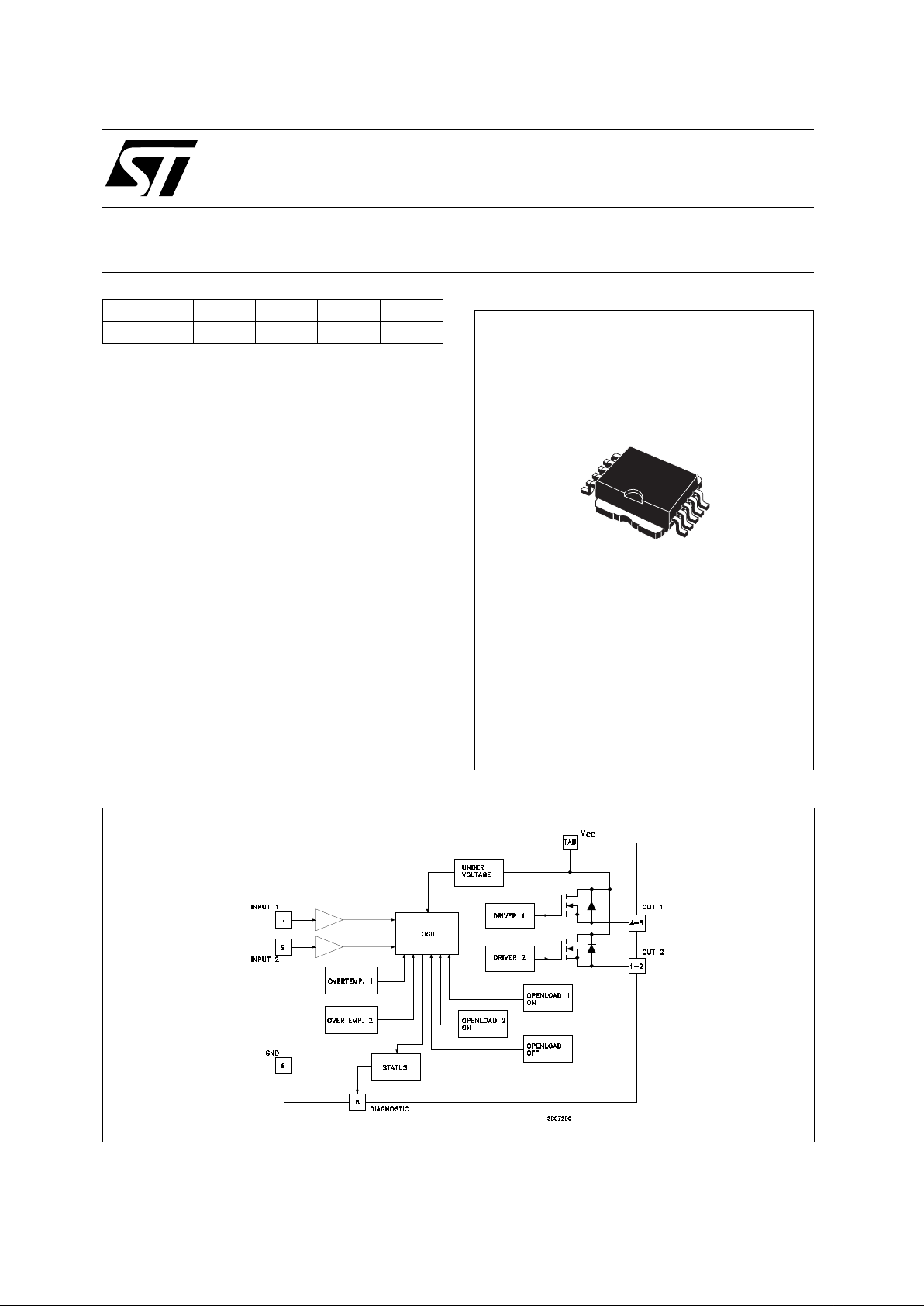
BLOCK DIAGRAM
TYPE V
DSS
R
DS(on
)I
OUT
V
CC
VND05BSP 40 V 0.2
Ω
1.6 A 26 V
■
OUTPUT CURRENT (CONTINUOUS) :
9A @ T
c
= 85oC PER CHANNEL
■
5V LOGIC LEVEL COMPATIBLE INPUT
■
THERMAL SHUT-DOWN
■
UNDER VOLTAGE PROTECTION
■
OPEN DRAIN DIAGNOSTIC OUTPUT
■
INDUCTIVE LOAD FAST
DEMAGNETIZATION
■
VERY LOW S T AN D-BY POWE R
DISSIPATION
DESCRIPTION
The VND05BSP is a monolithic device made
using STMicroelectronics VIPower Technology,
intended for driving resistive or inductive loads
with one side grounded. This device has two
channels, and a common diagnostic. Built-in
thermal shut-down protects the chip from over
temperature and short circuit.
The status output provides an indication of open
load in on state, open load in off state,
overtemperature conditions and stuck-on to V
CC
.
1
10
PowerSO-10
®
1/9
Page 2
ABSOLUTE MAXIMUM RATING
Symbol Parameter Value Unit
V
(BR)DSS
Drain-Source Breakdown Voltage 40 V
I
OUT
Output Current (cont.) at Tc = 85 oC9A
I
OUT
(RMS) RMS Output Current at Tc = 85 oC and f > 1Hz 9 A
I
R
Reverse Output Current at Tc = 85 oC-9A
I
IN
Input Current
±
10 mA
-V
CC
Reverse Supply Voltage -4 V
I
STAT
Status Current
±
10 mA
V
ESD
Electrostatic Discharge (1.5 kΩ, 100 pF)
2000 V
P
tot
Power Dissipation at Tc = 25 oC 59 W
T
j
Junction Operating Temperature -40 to 150
o
C
T
stg
Storage Temperature -55 to 150
o
C
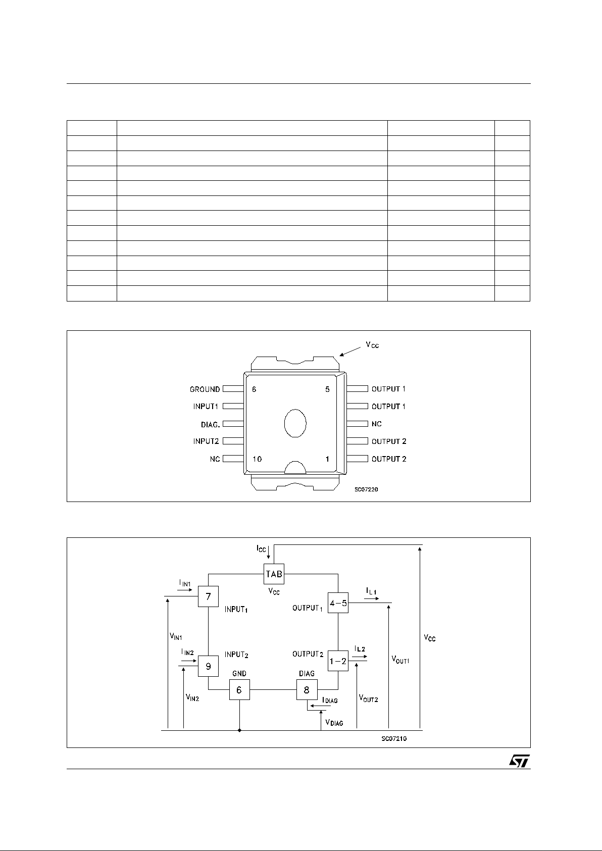
CONNECTION DIAGRAMS
CURRENT AND VOLTAGE CONVENTIONS
VND05BSP
2/9
Page 3

THERMAL D AT A
R
thj- case
R
thj-amb
Thermal Resistance Junction-case Max
Thermal Resistance Junction-ambient ($) Max
2.1
50
o
C/W
o
C/W
($) When mounted using minimum recommended pad size on FR-4 board
ELECTRICAL CHARACTERIST ICS
(8 < V
CC
< 16 V; -40 ≤ Tj ≤ 125 oC unless otherwise specified)
POWER
Symbol Parameter Test Conditions Min. Typ. Max. Unit
V
CC
Supply Voltage 6 13 26 V
In(*) Nominal Current
T
c
= 85 oC V
DS(on)
≤ 0.5 VCC = 13 V
1.6 2.6 A
R
on
On State Resistance I
OUT
= In VCC = 13 V Tj = 25 oC 0.13 0.2
Ω
I
S
Supply Current Off State Tj = 25 oC VCC = 13 V 35 100
µ
A
V
DS(MAX)
Maximum Voltage Drop I
OUT
= 7.5 A Tj = 85 oC VCC = 13 V 1.44 2.3 V
R
i
Output to GND internal
Impedance
Tj = 25 oC 5 10 20 K
Ω
SWITCHING
Symbol Parameter Test Conditions Min. Typ. Max. Unit
t
d(on)
(^) Turn-on Delay Time Of
Output Current
R
out
= 5.4
Ω
5 25 200
µ
s
tr(^) Rise Time Of Output
Current
R
out
= 5.4
Ω
10 50 180
µ
s
t
d(off)
(^) Turn-off Delay Time Of
Output Current
R
out
= 5.4
Ω
10 75 250
µ
s
t
f
(^) Fall Time Of Output
Current
R
out
= 5.4
Ω
10 35 180
µ
s
(di/dt)onTurn-on Current Slope
R
out
= 5.4
Ω
0.003 0.1 A/µs
(di/dt)
off
Turn-off Current Slope
R
out
= 5.4
Ω
0.005 0.1 A/µs
LOGIC INPUT
Symbol Parameter Test Conditions Min. Typ. Max. Unit
V
IL
Input Low Level
Voltage
1.5 V
V
IH
Input High Level
Voltage
3.5 (•)V
V
I(hyst.)
Input Hysteresis
Voltage
0.2 0.9 1.5 V
I
IN
Input Current VIN = 5 V Tj = 25 oC 30 100
µ
A
V
ICL
Input Clamp Voltage IIN = 10 mA
I
IN
= -10 mA
56
-0.7
7V
V
VND05BSP
3/9
Page 4

ELECTRICAL CHARACTERIST ICS
(continued)
PROTECTION AND DIAGNOSTICS
Symbol Parameter Test Conditions Min. Typ. Max. Unit
V
STAT
Status Voltage Output
Low
I
STAT
= 1.6 mA 0.4
V
V
USD
Under Voltage Shut
Down
3.5 4.5 6
V
V
SCL
Status Clamp Voltage I
STAT
= 10 mA
I
STAT
= -10 mA
56
-0.7
7
V
V
T
TSD
Thermal Shut-down
Temperature
140 160 180
o
C
T
SD(hyst.)
Thermal Shut-down
Hysteresis
50
o
C
T
R
Reset Temperature 125
o
C
V
OL
Open Voltage Level Off-State (note 2) 2.5 4
5V
I
OL
Open Load Current
Level
On-State 5
180 mA
t
povl
Status Delay (note 3) 5
10 µs
t
pol
Status Delay (note 3) 50 500
2500 µs
(*) In= Nominal current according to ISO definition for high side automotive switch (see note 1)
NOTE = (^) See switching time waveform
NOTE = (•) The V
IH
is internally clamped at 6V about. It is possible to connect this pin to an higher voltage via an external resistor
calculated to not exceed 10 mA at the input pin.
NOTE = note 1: The Nominal Current is the current at T
c
= 85 oC for battery voltage of 13V which produces a voltage drop of 0.5 V
NOTE = note 2: I
OL(off)
= (VCC -VOL)/ROL
note 3:t
povl tpol
: ISO definition.
Note 2 Relevant Figure Note 3 Relevant Figure
VND05BSP
4/9
Page 5

FUNCTIONAL DESCRIP TION
The device has a diagnostic output which
indicates open load in on-state, open load in
off-state, over temperature conditions and
stuck-on to V
CC
.
From the falling edge of the input signal, the
status output, initially low to signal a fault
condition (overtemperature or open load
on-state), will go back to a high state with a
different delay in case of overtemperature (tpovl)
and in case of open open load (tpol) respectively.
This feature allows to discriminate the nature of
the detected fault. To protect the device against
short circuit and over current condition, the
thermal protection turns the integrated Power
MOS off at a minimum junction temperature of
140
o
C. When this temperature returns to 125 oC
the switch is automatically turned on again. In
short circuit the protection reacts with virtually no
delay, the sensor being located inside the Power
MOS area. An internal function of the devices
ensures the fast demagnetization of inductive
loads with a typical voltage (V
demag
) of -18V. This
function allows to greatly reduces the power
dissipation according to the formula:
P
dem
= 0.5 • L
load
•(Ι
load
)2 • [(VCC+V
demag
)/V
demag
]
•
f
where f = switching frequency and
V
demag
= demagnetization voltage.
The maximum inductance which causes the chip
temperature to reach the shut-down temperature
in a specified thermal environment is a function of
the load current for a fixed V
CC
, V
demag
and f
according to the above formula. In this device if
the GND pin is disconnected, with V
CC
not
exceeding 16V, it will switch off.
PROTECTING THE DEVICE AGAINST
REVERSE BATTERY
The simplest way to protect the device against a
continuous reverse battery voltage (-26V) is to
insert a Schottky diode between pin 1 (GND) and
ground, as shown in the typical application circuit
(fig.3).
The consequences of the voltage drop across this
diode are as follows:
If the input is pulled to power GND, a negative
voltage of -V
f
is seen by the device. (Vil, Vih
thresholds and Vstat are increased by Vf with
respect to power GND).
The undervoltage shutdown level is increa- sed
by Vf.
If there is no need for the control unit to handle
external analog signals referred to the power
GND, the best approach is to connect the
reference potential of the control unit to node [1]
(see application circuit in fig. 3), which becomes
the common signal GND for the whole control
board avoiding shift of V
ih
, Vil and V
stat
. This
solution allows the use of a standard diode.
Switching Time Waveforms
VND05BSP
5/9
Page 6

TRUTH TABLE
INPUT 1 INPUT 2 OUTPUT 1 OUTPUT 2 DIAGNOSTIC
Normal Operation L
H
L
H
L
H
H
L
L
H
L
H
L
H
H
L
H
H
H
H
Under-voltage X X L L H
Thermal Shutdown
Channel 1
HXLX L
Channel 2
XHXL L
Open Load
Channel 1
H
L
X
L
H
L
X
L
L
L(**)
Channel 2
X
L
H
L
X
L
H
L
L
L(**)
Output Shorted to V
CC
Channel 1
H
L
X
L
H
H
X
L
L
L
Channel 2
X
L
H
L
X
L
H
H
L
L
(**) with additional external resistor.
Figure 1:
Waveforms
VND05BSP
6/9
Page 7

Figure 3:
Typical Application Circuit With Separate Signal Ground
Figure 2:
Typical Application Circuit With A Schottky Diode For Reverse Supply Protection
VND05BSP
7/9
Page 8

DIM.
mm. inch
MIN. TYP MAX. MIN. TYP. MAX.
A 3.35 3.65 0.132 0.144
A (*) 3.4 3.6 0.134 0.142
A1 0.00 0.10 0.000 0.004
B 0.40 0.60 0.016 0.024
B (*) 0.37 0.53 0.014 0.021
C 0.35 0.55 0.013 0.022
C (*) 0.23 0.32 0.009 0.0126
D 9.40 9.60 0.370 0.378
D1 7.40 7.60 0.291 0.300
E 9.30 9.50 0.366 0.374
E2 7.20 7.60 0.283 300
E2 (*) 7.30 7.50 0.287 0.295
E4 5.90 6.10 0.232 0.240
E4 (*) 5.90 6.30 0.232 0.248
e 1.27 0.050
F 1.25 1.35 0.049 0.053
F (*) 1.20 1.40 0.047 0.055
H 13.80 14.40 0.543 0.567
H (*) 13.85 14.35 0.545 0.565
h 0.50 0.002
L 1.20 1.80 0.047 0.070
L (*) 0.80 1.10 0.031 0.043
α
0º 8º 0º 8º
α
(*) 2º 8º 2º 8º
PowerSO-10™ MECHANICAL DATA
(*) Muar only POA P013P
DETAIL "A"
PLANE
SEATING
α
L
A1
F
A1
h
A
D
D1
= =
= =
E4
0.10 A
E
C
A
B
B
DETAIL "A"
SEATING
PLANE
E2
10
1
eB
HE
0.25
P095A
VND05BSP
8/9
Page 9

Information furnished is believed to be accurate and reliable. However, STMicroelectronics assumes no responsibility for the consequences
of use of such inform ation nor for a ny in fringem ent of paten ts or other rights o f third par ties wh ich may result from its use . No l i cen se i s
granted by implication or otherwise under any patent or patent rights of STMicroelectronics. Specification mentioned in this publication are
subject to change without notice. This publication supersedes and replaces all information previously supplied. STMicroelectronics products
are not authorized f or use as critical components in life support devices or systems without express written approval of STMicroelectronics.
The ST logo is a trademark of STMicroelectronics
© 2000 STMicroelectro nics – Printed in Italy – All Rights Reserved
STMicroelectronics GROUP OF COMPANIES
Australia - Brazil - China - Finland - France - Germany - Hong Kong - India - Italy - Japan - Malaysia - Malta - Morocco -
Singapore - Spain - Sweden - Switzerland - United Kingdom - U.S.A.
http://www.st.com
VND05BSP
9/9
 Loading...